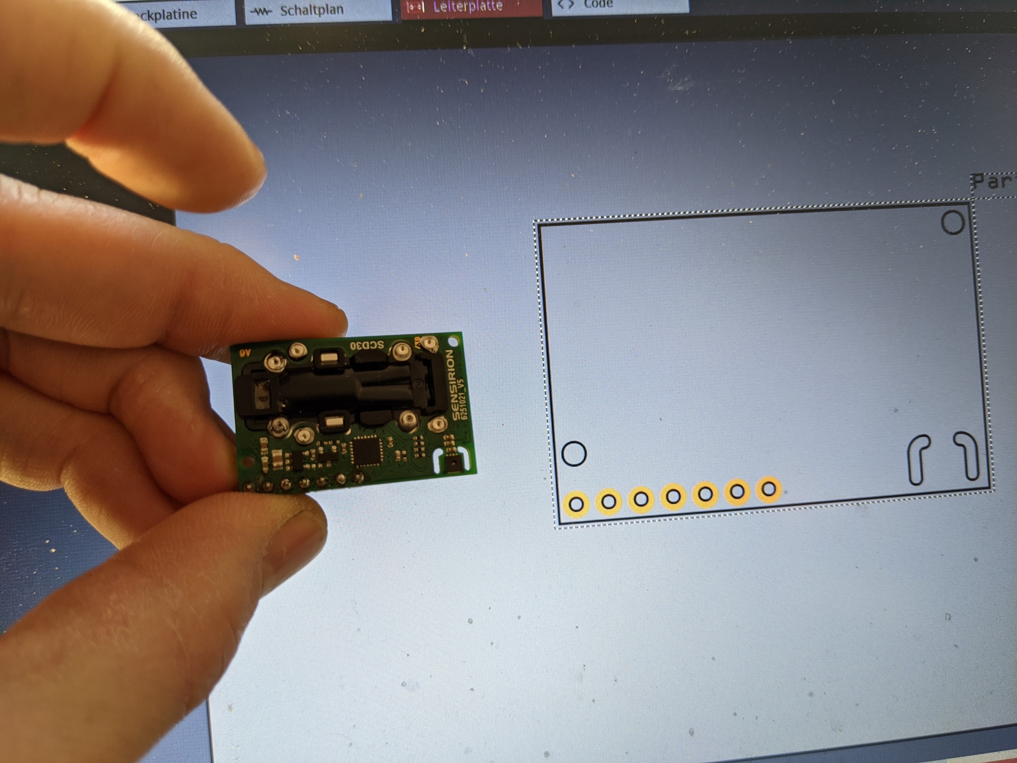
Hi everybody, I’ve just started to use fritzing and already dared to make my own part as I wasn’t able found a fritzing file for the SCD30 sensor - despite all the documents available at the manufacturer’s website.
So, I am sure made a lot of mistakes (although walking through all those tutorials was certainly helpful, thanks to the community for the effort!), but the part seems to work for me, so I would like to hear your comments, so I can improve the part
The fritzing file for that part can be found on github - or is uploading it directly the preferred method?
And how is the procedure to let the component find its way into the fritzing library?
The youtube video you inserted and a wikipedia-page just told me that Gerber is a file format used for PCB design. If I open the parts editor, PCB view and then Export → for Production → Extended Gerber it says:
“Your sketch does not have a board yet! Please add a PCB in order to export to Gerber.”
But that also happens when I open one of the other pre-defined parts with the part editor. I’m sorry, but I don’t understand therefore how that is related to the correctness of the single part…? (In my understanding the Gerber-Check should be performed for your full setup, not for single parts?)
Yes, the gerber export is for the current sketch, which typically has multiple parts with traces between connectors. As a minimal test for your part file, create a new sketch document, place the part, add a few connecting wires, then try the export.
I just did as you suggested, and it looks OK to me (thanks to @Old_Grey for his detailed video!). Any next step I should perform to further ensure the part is OK?
Even though it gerbers I didn’t check the dimensions, so make sure it is right before you get any PCB made that this part plugs into, ie, print out the PCB and see if the part plugs into the paper.
EDIT - if you watch all that vid it explains why it’s so important.
Summary: There are several breaking errors in this version of the part too. As well as additional cosmetic problems that should be cleaned up.
I ran the contents of that part file through FritzingCheckPart. Here is a summary of what it reported, and what I noticed doing a manual inspection and smoke test in Fritzing.
There are ‘px’ units on font-size attributes in the schematic view svg file that Fritzing is known to not handle well. The text size can change from what was intended. Fritzing wants just numbers, without units. Fritzing wants just numbers, without units. Using ‘px’ units is valid for the svg format specification, but Fritzing does not handle it.
The new convention is to use black graphics for pcb silkscreen, instead of white. Fritzing automatically converts (and so does the FritzingPartsCheck tool), but for future reference, black is preferred for the silkscreen of pcb svg files.
The fzp part definition file does not have a “fritzingVersion” attribute for the module element. The handling of some part details has changed over time (older versions of Fritzing), and the value of the version is used to choose which way certain things are interpreted. A value of “0.9.4b” should tell Fritzing to use the (currently) latest rules. Fritzing Parts Editor automatically fills in the full version number. When manually creating parts files, a shorten version is good enough.
The connectors in the part have been configured with the type set to “female”. Except for parts that act like breadboard, and some ‘shield’ or ‘hat’ parts, that is normally better as “male”. The connectors need to be “male” to all the part to be dragged onto a breadboard, and automatically connect. With “female”, other (male) parts will automatically connect to this part when the connectors line up. Without using any wires. Which way this should be implemented depends on the part (and user preferences), but using “male”, and allowing the part connectors to link to breadboard connectors is the usual expectation.
A warning is being reported about an “-inkscape-font-specification” with an invalid value. As long as the standard svg “font-family” entry also exists, the inkscape specific extension can be safely ignored.
The “breadboard” layerId specified in the fzp part definition does not exist in the matching svg image. This will “appear” to work in Fritzing, but exporting a sketch to an svg image will not include the part. The “breadboard” id should be added to the first/outer wrapper group element. Currently there is not wrapper group, so it should be created. Select all, create group, in Inkscape.
The same problem exists for the “schematic” layerId and matching schematic svg file.
The part definition shows terminalId attributes for connectors in the breadboard view, which do not actually exist in breadboard svg. If the terminalId is defined, a matching graphic element should exist in the svg.
Normally, a terminalId is not needed for breadboard view connectors. Especially when the connections are just header pins. An edge connector might need one.
The part definition shows terminalId attributes for connectors in the schematic view, which do not actually exist in schematic svg. These should exist in the svg. They are used to give Fritzing a reference point, to “snap” wires to. Without this, wires attached to the connectors will be drawn to the middle of the connector pin line, instead of to the end.
There is a graphic element at the start of the pcb svg file, that is not in any of the layerIds specified in the fzp file. It is probably intended to be part of the silkscreen. As is, it will not be included in any export of the pcb view.
The fzp definitions show both copper1 and copper0 layerIds for the pcb view. That normally indicates that the part is through hole. However, the pcb svg file only contains a copper1 layer (group). There is no ‘bottom’ copper for the connectors. So the pcb information has this as an SMD part.
FCP also complains that the pcb connectors do not have a radius, which means that no hole will be drilled. If this is really an smd part, the connectors should be drawn as filled pads. This visually look like circular holes with copper rings around them, but that is not what will be exported to gerber. If these are supposed to be through hole connectors, the “connector«n»pin” elements should be circle elements. The radius of the circle, combined with the thickness of the stroke determine the hole size. Non-circular copper rings can be create by adding additional elements, but the circle needs to exist to get a hole drilled.
The connector pin lines in the schematic view should be a standard color, not colorized by function.
All connector pins in the schematic view should align to a 0.1 inch grid. Because the terminalId elements are missing, the part is aligning to the center or the lines, instead of the ends.
Several of the connector descriptions in the fzp file seems to be overly verbose. Having details is good, but try to keep it to only enough to understand what the connector is for. Not the complete history, and how to use it.
it was mirrored (so you had to use bottom for top) and the holes were to small so my 1/32 inch (0.8) mill could not mill the holes and the copper ring was very small. Also better to have copper rings on both sides. The part works for me now but we will try to fix the errors.
I saw you on Freie Maker. Nice to meet you! Below you see your part on top.
I would agree that the copper pads are too small in the original.
But the mirroring is the other way around. The original part actually has the correct orientation, while you apparently intent to mount the sensor bottomside-up onto the PCB, so now the footprint is flipped.
Which exposes an interesting problem. Fritzing’s PCB view does not offer the possibility to flip a part, like it does by default in schematic view and like it can be enabled in breadboard view. Which makes sense for classic components. But for breakout boards one could actually decide to mount it upside-down, like in this case. Which would require being able to flip the footprint. Also in the case of double-sided assembly this would be needed. Certainly not the most common case, but how far fetched is it really?
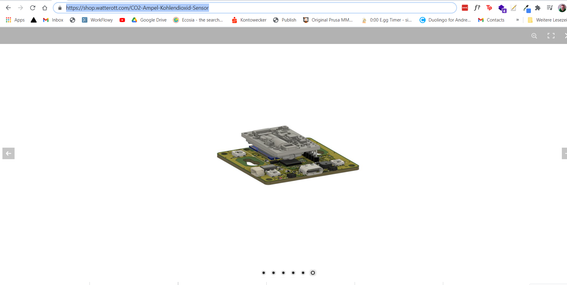
No your original part is flipped. Look here at watterot they also mount it like we mounted it. This way the LED is visible and the humidity/temperature sensor is on top and you can design a case for it. Also the seedstudio grove SCD30 board is mounting it like that. Do you want to argue that all these professionals made a mistake but you that did a part the first time and did such a project for the first time are right?
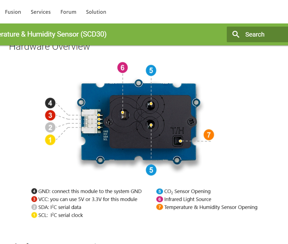
The OP linked to the website of the manufacturer of the sensor, from where the data sheet for this sensor is available. This data sheet clearly states what is the top-view and what is the bottom-view. I would say that the original part is based on this data sheet, and therefore correct. The breadboard view shows the top view, and so does the PCB view.
If everybody decides that the sensor should be mounted bottom-up, fine. If that is what makes the most sense, sure. I would want to argue, though, that the better approach for everyone following later and wanting to use this part would then be to create a new part which is explicitly this sensor turned around. Which means, PCB view is bottom-view and breadboard view is bottom-view. Which, of course, involves a lot more work to create a new BB SVG. So that doesn’t make sense if all one wants is a quick way to use this part in PCB view, mounted bottom-up.
This provides a new aspect to the more interesting question, whether PCB view should allow to flip parts. Right now BB view can do it, but the part image is simply mirrored. It’s not like its flipped around and then shows a bottom view image of the part. Since that is possible and already deviates from the maxim to mirror reality, then PCB view should probably allow it, too, where it would actual real sense, as seen in this example here.