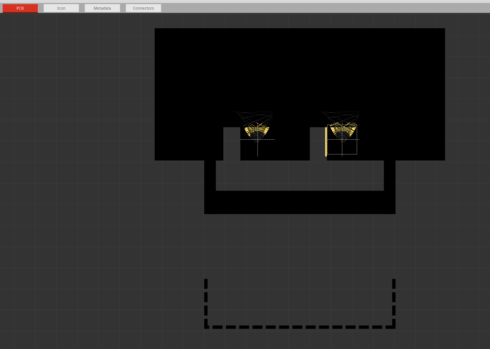
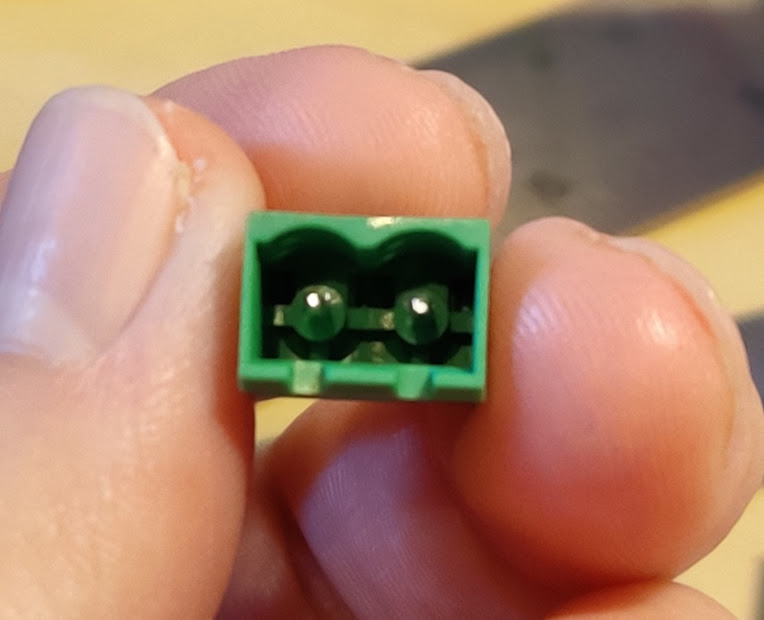
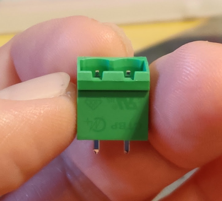
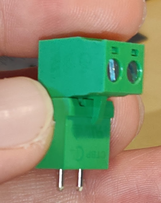
Currently I’m using something quite similar to this (Camdenboxx_CTB0158-8), but the PCB footprint isn’t the same (the CB part has a 90degree input for the wire, whereas the RS part is a push in the top), I thought maybe this would be a good part to be the first I make in Fritzing. That said there seems to be a lot of graphics work in the CB part.
There’s also multiple termainal sizes on this part (I’m using the 2 & 8 right now) so that would be good to work into the part too, but that also seems more complex for my first one.
Would this be simple enough for me to get started on? I’m feeling bad about all the parts you guys have made for me up to now so I’m trying to get stuck in!
I’d probably start with the 2 position ones as being easiest (the 8 can be produced by copy/paste of the 2 pin version.) I see there is a footprint of some kind available which may make things easier, because there doesn’t look to be a data sheet available. These two sets of tutorials are probably a good place to start from the Fritzing end:
So I’ve made some small tweaks to the silkscreen of the AQT212GH part you made for me Peter so it’s a little more representative of the footprint, so that’s a start!
As for this part, I went to the camdenboss part (open in new parts editor) but the ‘show in folder’ option just takes me to the ‘my documents’ folder on windows, not the folder containing the svg file for this part.
I’m guessing that’s linked to the other linux issue we were having with this part?
Anyway I should be able to find it, but thought I’d raise that as a potential bug.
Ah, I meant to say that as you can see on the attached SVG the ‘silkscreen’ xml group is above the copper one as I believe it’s meant to be, and it appears behind the solder pads as it’s meant to, but in fritzing the silkscreen appears on top of the copper pads.
Additonally can you tell me how I can package up these svgs so that the whole part (breadboard, schematic, pcb) can be added to a new fritzing users’s parts?
Thanks for the heads up, just to confirm you’re saying the same exact item on RS for this product can vary? Or that there are two similar items so be wary of what I buy?
Camden make the same connector with strait and 90o that look the same green colour but they come in two variants of pitch we used to have two bins that were next to each other on the rack so I had to move one as my girl would pick up the wrong one when doing boards as they look the same I did ask Camden to make a colour change but no go so be careful when you order
All the best Bob
ah, gotcha, thanks for the heads up then. @vanepp or others I’ve made this SVG which is pretty good in inkscape, but it’s not looking right in Fritzing, what is wrong with the SVG please?
I see nothing wrong with the svg itself. The path element that is used to draw the shape of the top part of the silkscreen is overly complex. It is valid, but it is possible that Fritzing is choking either on the size of it, or on some part of it. Those curved sections are being defined with a LOT of small arc segments. That should be able to be reduced to 2 cubic curves. Try this (not tested in Fritzing)
This should not affect the graphical display, but I am not sure that Fritzing handles a connector pin as a group element. What I see usually, is the connector pin id on the circle element, and the rect element that turns it into square is picked up automatically.
Unfortunately though that’s not a lot better in Fritzing.
To make the circle cut outs I made a rectangle and two circles, and then ‘Path --> Division’ to cut the circles away from the rectangle. Perhaps that isn’t the best way to achieve this affect? Is there a more Fritzing friendly way?
Also @microMerlin could you tell me why you wrapped the ‘copper0’ group in the ‘g9’ group please?
That was on the original SVG I used to model this component but I didn’t see anything about this in the tutorials from what I recall, just the copper0 (and 1) and silkscreen groups.
I did not add the g9 wrapper element. It was already there in the file you posted, and I was being careful to only change the single 8316 character long path element. I assume it was there from where ever you got it from. Given that partID attribute that is also on the wrapper element, I expect that it was taken from an export of the pcb view of a sketch.
The transform was because the connectors (block) was rotated 90 degrees. svg transform attributes have been known to cause issues with Fritzing. Here is the svg again, this time also without that transform. I left the wrapper around the rectangle and circle elements that make up connector0pin.
The usual way I have seen the rectangular connectors created is with a filled path that contains an interior cutout overlaid on a slightly smaller circle (so the path extends beyond the outer edge of the circle, and does not reach the inner edge). Instead of a hollow rect overlaid on a circle. I have not explored other options, so I do not know if Fritzing cares. If it does care, I would expect problems with design rules check and/or gerber exports, not with the visual display.
To create a path object like that in Inkscape, place a standard filled ellipse over a rectangle, select them both, and use the Difference command on the Path menu.
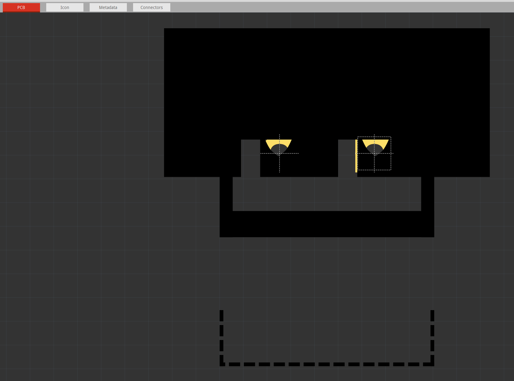
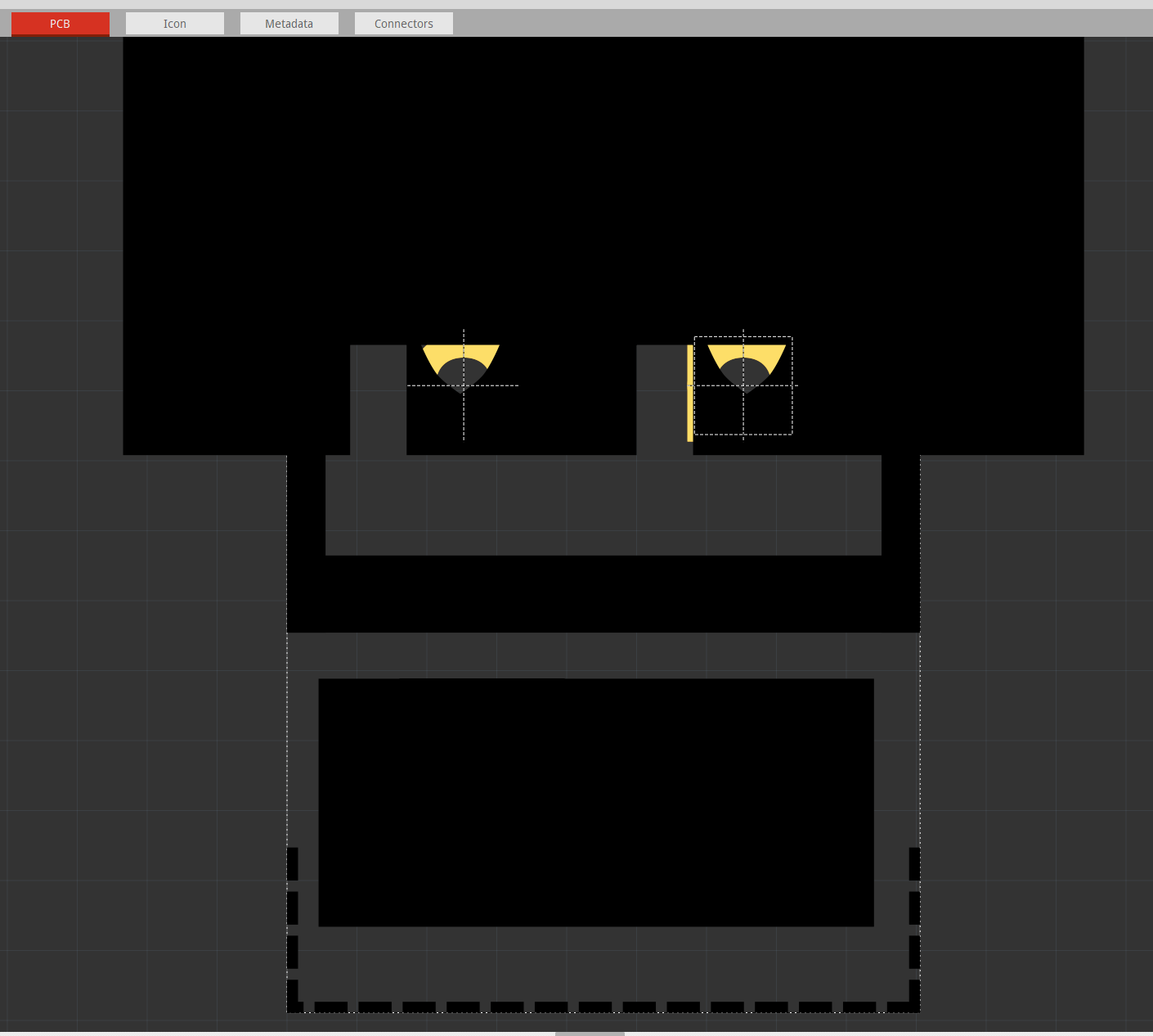
I’ve found though that both difference and division techniques look fine in ‘breadboard’ view in fritzing, so something is off with the PCB section of fritzing.
What’s the best way to report this as a bug? For the time being I’ll just have to not show the circles.
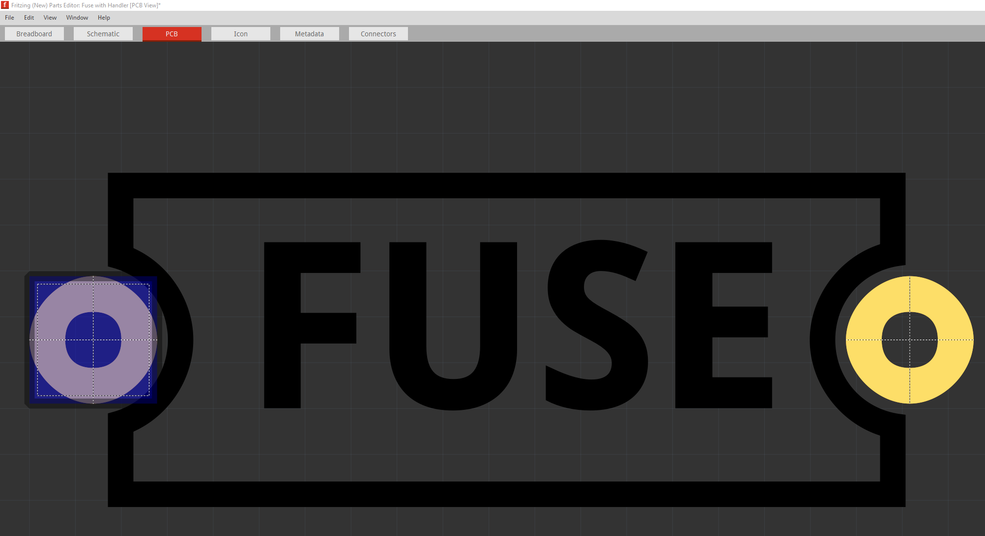
FYI I was wondering what’s different about this core fuse component, as it has circle cut outs and looks fine on PCB view, though I’m unabe to upload it’s SVG for some reason.
If you upload the complete part file, we can have a look to see what interactions there might be between Fritzing, the part definition, and the svg file. I can’t really say it is a bug yet. Or maybe just a bug in some piece of the documentation for parts creation. Or something else entirely.
Which fuse component? A search of the parts library for “fuse” gets 7 matches. None of which seem to have what I think of as circle cutouts. A problem with a difference between what each of us mean by the term? Through hole connection pads are not cutouts. They are just a circle element with a stroke size that are not filled in. I think of a cutout as an arbitrary shape (not a circle) that has a circle (or ellipse) cut out of the interior. In the latest screen shot, that looks like the circle was overlapping the edge of the rectangle when the cut was done. Not inside the rectangle. A hollow (stroke but no fill) rectangle with a circle element sitting on top is also not a cutout.
Like I say though it’s not the end of the world so honstly I’ll just go for straight lines right now, it’s just a bit of a pain that I can’t trust what I see in Inkscape is what I’ll get in Fritzing, but now I know that I’ll be more cautious.
That is a standard through hole part. The connectors are circle elements with a stroke width. The circle radius minus half of the stroke with defines the hole size to be drilled (what you are calling the cutout?). The stroke width defines the size of the copper around the hole.
What makes you think these are not full circles?
Connector (pad) elements, must be created using svg circle elements to get the gerber export to specify that a hole needs to be drilled. If you use something else (ellipse or path with curve and/or arc), gerber will specify the copper, but not a hole. You can verify what Inkscape has done by selecting an element, and looking at the xml editor. For this purpose, straight lines are useless.
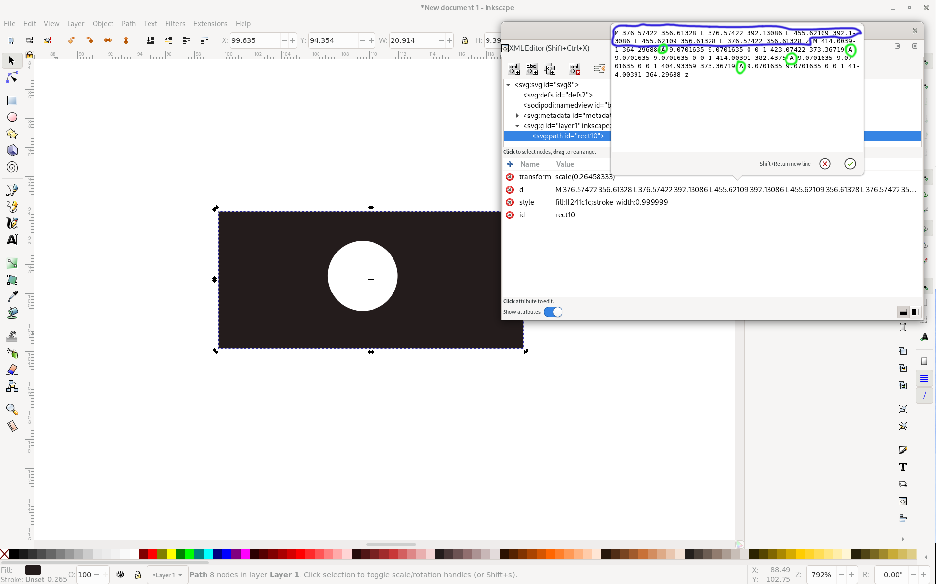
Here is a view of an Inkscape screen with what I mean by a cutout. This was created using the difference operation on a rectangle and a circle. It shows the created path object, the xml editor view of the object, and the data in the “d” attribute of the path element. The first part, up to the “z”, circled in blue, is the rectangle edges, converted to lines. The rest is the circle cut out inside of that, converted to arc (“A”) segments.