So back to Inkscape?
I think so, but I’m not sure what to do. The instructions say it needs to be a single shape (which you seem to have) but Fritzing doesn’t like it. Until we can get it to generate the correct board outline in the gerber output, the board can’t be produced. As noted I have never had any luck at getting board shapes to work so I’m not much help here. This is what the instructions say:
"Make sure you only have a single merged shape, not serveral distinct ones. If you want to display some guiding graphics (such as the location of the pin headers for the Arduino shield), you can add them as sublayers of “board”. In this case, make sure you give the board shape item itself the id “boardoutline”. "
Somewhere (perhaps in one of the forum posts on this subject) something about making the path differential. I think there was also something about the direction of the flow, but I never grasped any of it well enough to figure out how to do it. I expect our only hope is that someone who has had success making these will give us a hand to get an outline svg that works on Fritizng. Without that I don’t see how we can succeed.
Peter
Can you tell me what I am doing wrong here? This seems like it should create what we want, and apparently does in Fritzing, but even when I added the M commands to take both paths back to the start the gerber export still doesn’t work (n 0.9.9). I found this site that visualizes path commands and it seems happy enough with my additions (underlined in red here)
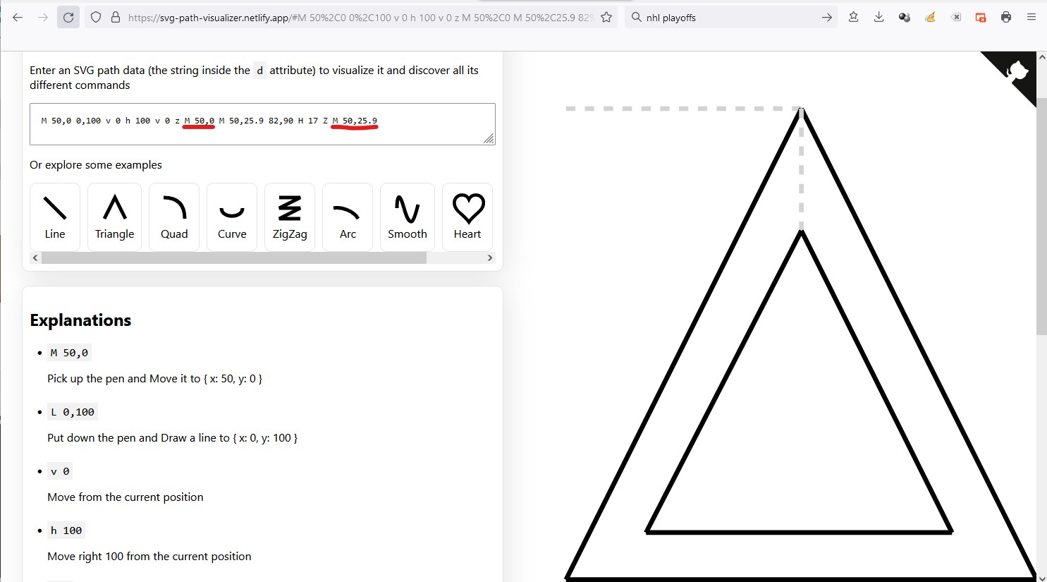
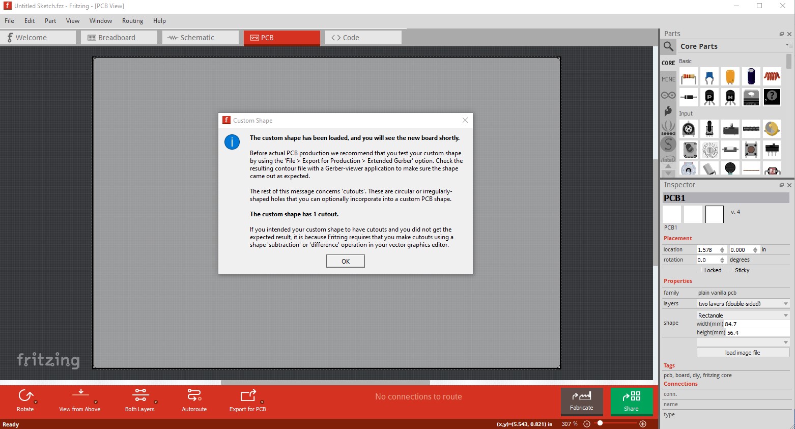
it renders the image as I expect. Fritzing seems happy with it and detects the cutout, so far so good:
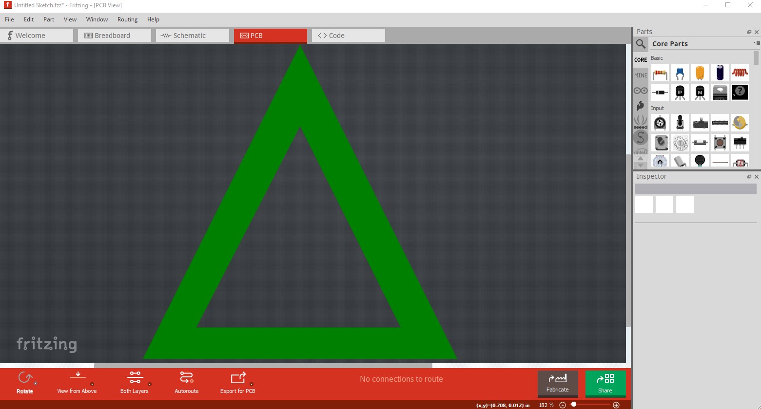
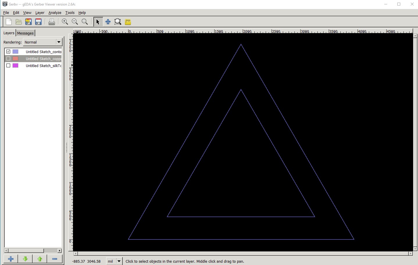
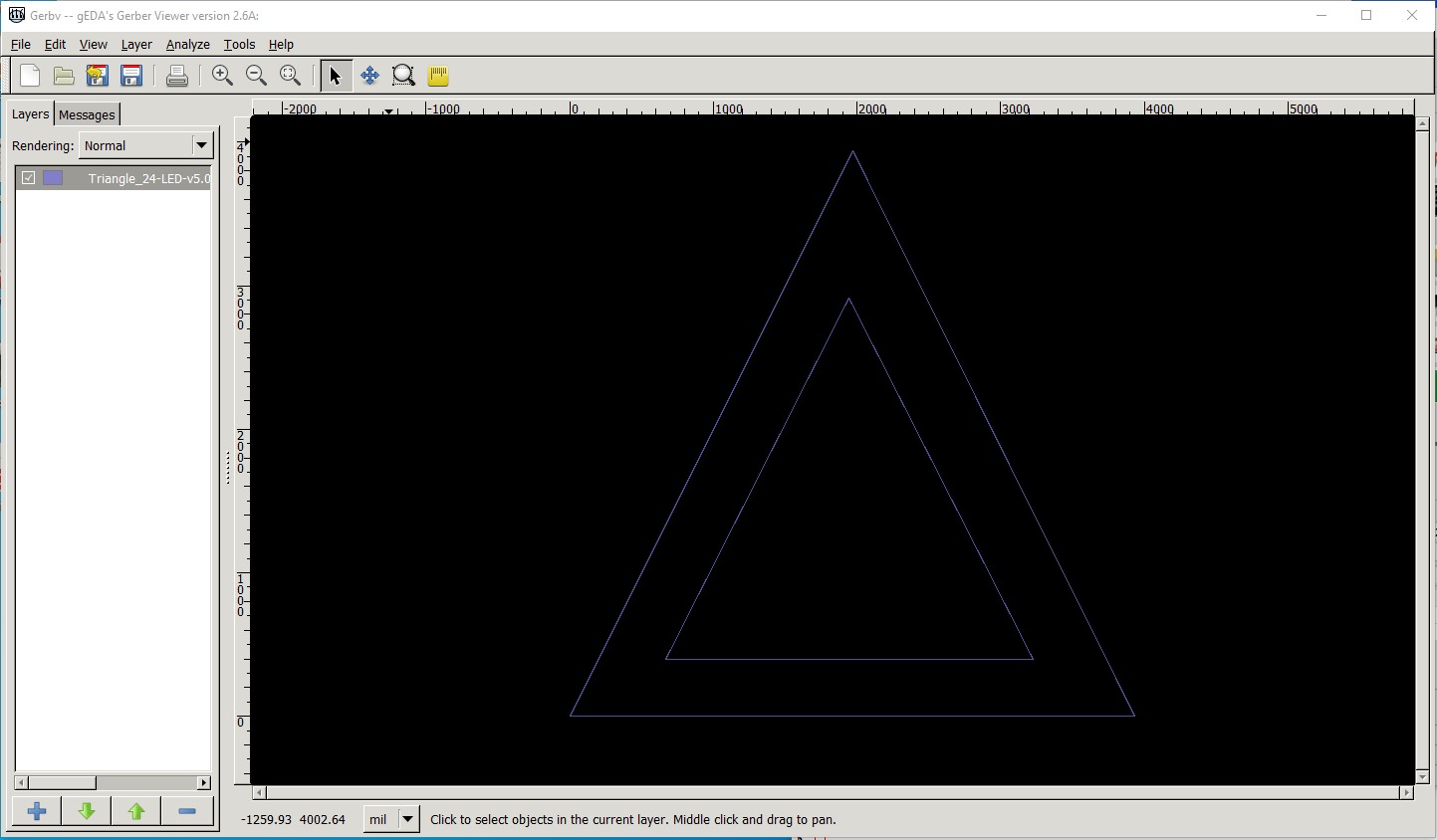
This looks to be what we want with sharp edges everywhere on the triangle. However gerber output is unhappy, it appears the paths are not completing (even with what I think are the commands to cause the path to complete!)

the contour.gm1file shows what I think is the path non completion bug despite the moves back to the start of the path. Can you suggest a work around? This is the svg that was used as the board outline above:

Is it possible it is unhappy about the svg not being “differenced”? I tried selecting that in Inkscape but it isn’t any more successful, but I also don’t know what I am doing! Until we can get the board outline to render correctly in the gerbers I don’t think this project can complete as the board won’t be correct. I’m out of ideas on how to fix it (but I am rarely successful with cutouts anyway  )
)
Peter
the boardout path contains
d="M 50,0 0,100 v 0 h 100 v 0 z M 50,0 M 50,25.9 82,90 H 17 Z M 50,25.9"
Each of the “v 0” sections does nothing. Should not break anything, but not needed. The “M 50,0” after the first “z” does not do anything. From the commentary in the post, the intent was to “force” the shape to close. That is not the way to do it. Instead, you need to explicitly add the line segment before the “z”, so (first part)
d="M 50,0 0,100 h 100 L 50,0 z"
same for the cutout shape in the second part
M 50,25.9 82,90 H 17 L 50,25.9 Z "
to get
d="M 50,0 0,100 h 100 L 50,0 z M 50,25.9 82,90 H 17 L 50,25.9 Z"
With the explict close like that (last point = first point), the “Z” should not be needed either, but should be safe.
The silkscreen element has stroke-width:0. With that, nothing gets drawn. Increasing that though is going to be wrong for the specified coordinates. Stroke extends both sides of the element, so would be half outside of the board.
I do not think any of that “defs” block is needed. Nothing references it.
I have been trying to create a usable svg from scratch (using a spreadsheet to calculate coordinates). It has not loading properly in Fritzing. Scaling is off. The custom shape shows the correct 100 x 86.6mm dimensions, but the triangle is only taking up the top left corner of that. Ruler says it is only about 28.5mm wide. I just found the problem. I had “viewbox” instead of “viewBox”. Now I can continue to the gerber tests.
Here is an equilateral triangle custom board svg that passes the gerber test. Give it a try in your environments.
I had to manually include the final “closing” segment for both the outer board and inner cutout. Interestingly, I did not need to do that for the silkscreen, which is also 2 closed triangles in a single path, but no cutout. It appears the problem is only with closing cutouts, not specifically the closing path shapes with “z”. I am using Fritzing 0.9.6, so that could have changed as well.

The silkscreen is almost invisible here, because it is white on white for the web page.
I generated the svg above using a spreadsheet. This triangle is 100mm on an edge, with 10mm wide sides. The silkscreen is 0.5mm thick. Any of that can be changed in the spreadsheet, then copy the svg block to an svg file with a standard text editor. Here is the spreadsheet, wrapped in a zip, and named to end in .fzz so the forum will accept it as an upload. Just save then unzip to recover the .xlsx spreadsheet.
pcb-svg-triangle.fzz (7.4 KB)
1 Like
Success! Thank you. On Fritzing 0.9.9 on Win 10 the gerber export now works correctly:
using this svg as the outline should do the trick and make the project work.
Peter
1 Like
Turns out what I asked for isn’t what I wanted The new svg with the triangle straightened, breaks the currently routed board:
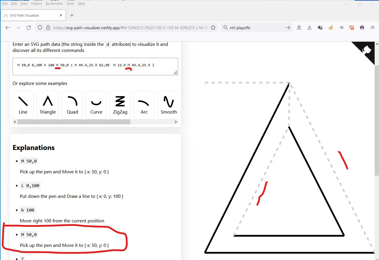
While I could move everything up, the angle of the LEDs would need to change. So I decided to doctor the original svg with the format from the corrected one. But everything I tried ended up with the two lines missing. Turns out SVG Path Visualizer is my friend! It tells me the Ms want to be Ls to draw the lines. Fritzing is doing the right thing when it doesn’t draw the two lines (at least according to SVG Path Visualizer) and it looks like Fritizing agrees because it works when I us Ls in place of the Ms.
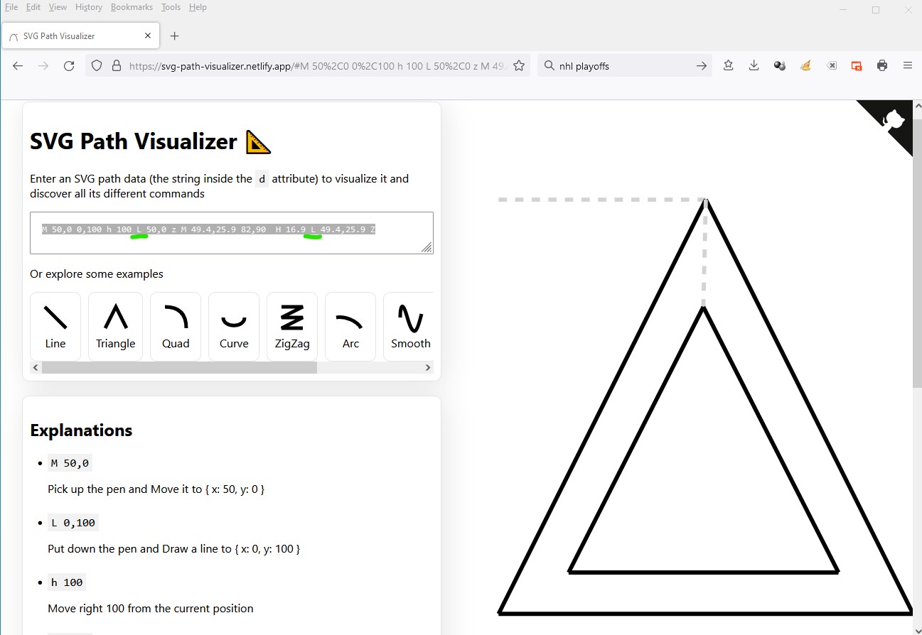
with the Ms instead of the Ls above, this output looks just like Fritzing, missing the two ending lines. Which makes sense to me because the M command says pick up the pen and move to these coords, not draw a line there (and of course using the L works!)
This is the modified svg that works:

both Ms are
M 50,0 0,100 h 100 L 50,0 z M 49.4,25.9 82,90 H 16.9 L 49.4,25.9 Z
and I set silkscreen stroke width to 0.1 as recommended in the outline instructions.
fill:none;stroke:#ffffff;stroke-width:0.1
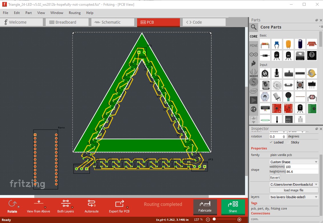
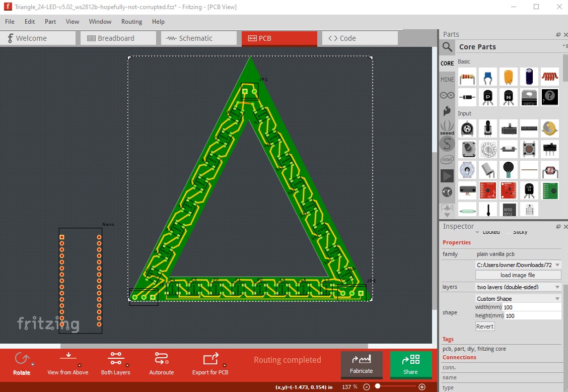
With that loaded as the image file the current layout is good, ready to have the bypass caps added and be cleaned up a little (fatten up the power traces!)
and it appears to correctly output as gerbers so it can be produced. This is the contour.gm1 file alone (to make sure it is right!)
and all the rest of the layers
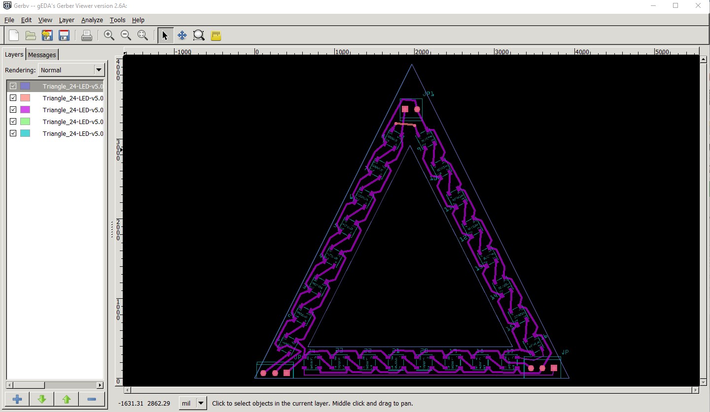
Now all that should be needed is to add in the bypass capacitors and vias, run the trace or dout on the bottom of the board so as to not impact the top side power runs and it should be ready to go.
Peter
1 Like
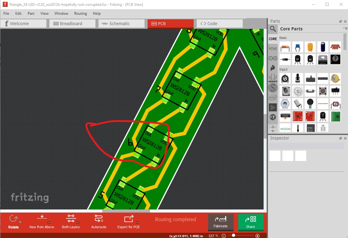
OK, so I have completed routing on the first side of the triangle (adding the necessary capacitors and vias), and corrected some errors, but an offset has crept in due to the new outline svg I think and you need to decide what to do about it. First the couple of errors:
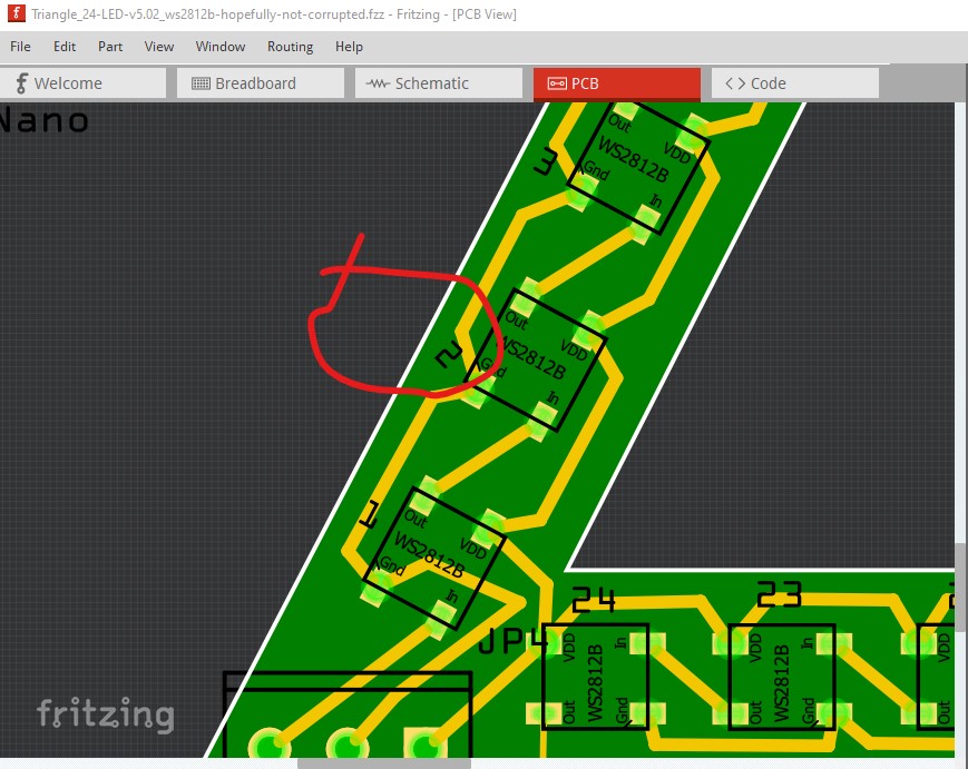
I don’t know how you did this (I had to delete minus the LED and replace it to correct it!) but the LED label is rotated relative to the LED on LED2 and LED6. Note I started the capacitors at C1 on LED1 so the capacitor number matches the LED number to make locating its position easy.
I think because of the kink in the bottom of the triangle (circled in red here) the position of the LEDs in the new version with the outline svg replaced are a little off. Here in your original sketch at the top the LED aligns with the ruler (which aligns with the edge of the triangle)
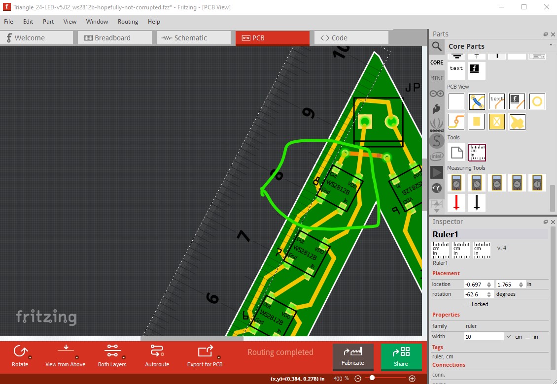
but by the bottom corner
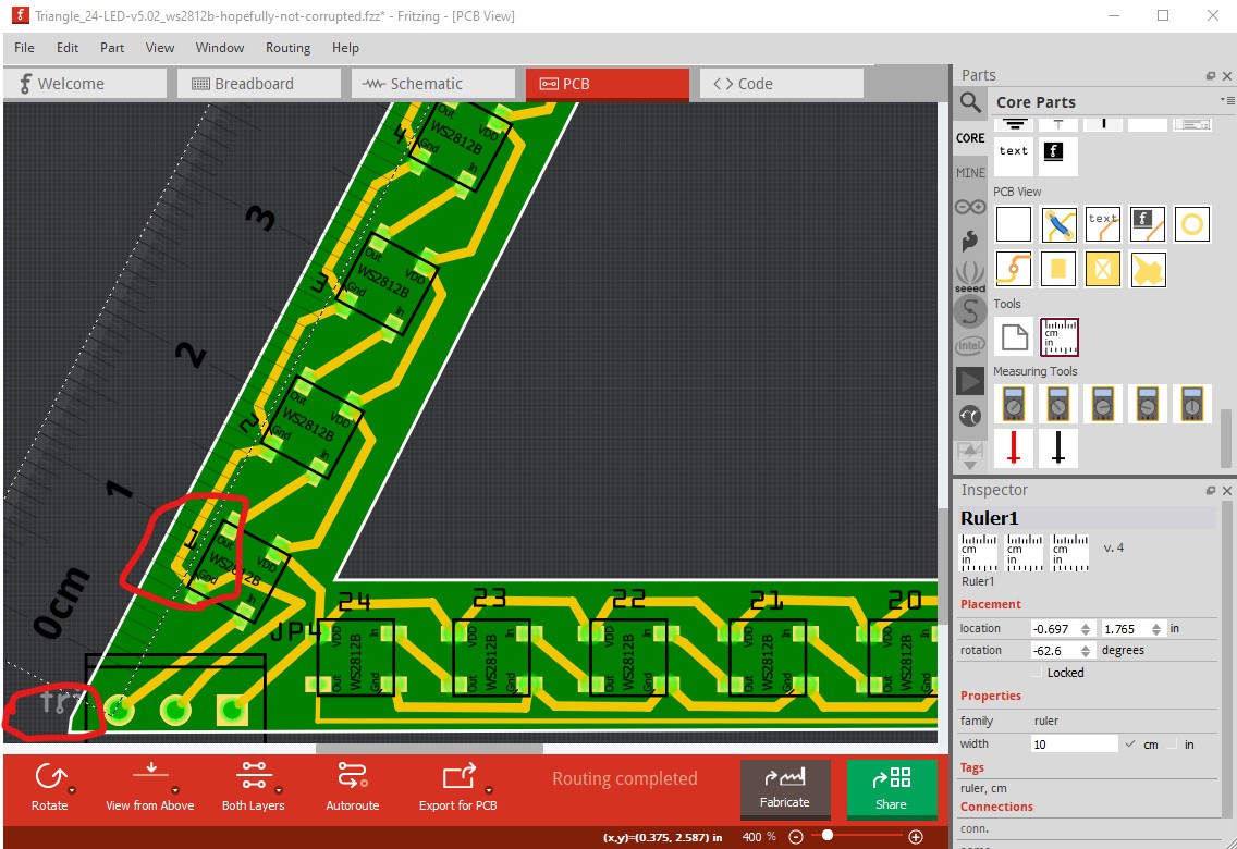
It is out a bit. With the new outline svg it is also out a bit.

The best bet would probably be to redo the calculations based on the new sketch (included below) so the spacing and angle of the LEDs is consistent and correct. I instead choose to rotate the LEDs to match the ruler (which may be less precise.) I’ll let you decide how you want to proceed. Here is the latest sketch with the new outline svg loaded and the first side of the triangle fully routed.
Triangle_24-LED-v5.02_ws2812b-new-latest.fzz (67.0 KB)
Peter
1 Like
Peter,
Thanks for all the hard work on this. I did try to redesign the image and had made it 10 cm x 10 cm. I don’t understand all the “m’s” and “l’s”. I’m away this weekend and didn’t bring the laptop with me, but when I get back I will dive back into it. And probably start from the start.
Thanks again, and to @microMerlin for the help.
Another weird one.
Scott
For all sorts of details about the possible “command” characters, see
for quick summary, “m” is move relative, “M” is move absolute, “l” is draw line relative, “L” is draw line absolute.
As a side note, with the 10cm equilateral triangle with 1 cm side width, the leds can be centred and evenly spaced at 1cm intervals all the way around, including where it turns the corners. Basically, every 1 cm around a 9cm equilateral triangle, except the corners. The 2 closest to a corner end up 1cm apart as well.
1 Like
Attached is one with all of the capacitors placed. It passed the DRC check.
Do I need to place a capacitor after led24?
Can I replace the jumpers with vias so wires can be soldered on the holes?
Triangle_24-LED-v7.06-no-jumpers.fzz (78.2 KB)
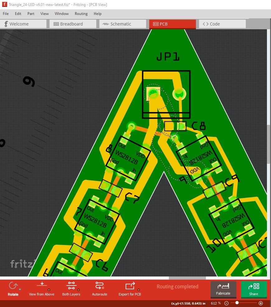
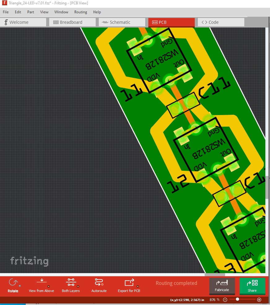
Looks good! First I completed routing in schematic, so I will be alerted if any of the changes I make in pcb are incorrect. Turning to pcb view I double clicked on the trace at the green arrow to simplify the route and increase the width of the trace because this is a power wire and we want the path to be as simple and wide as it can be.
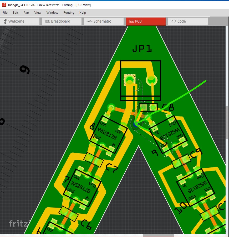
which turns up a problem in that the wire isn’t properly connected (and
thus won’t route correctly in schematic although it will work just fine in pcb!):
so route it on the shortest route and increase its size to a 48mil trace width.
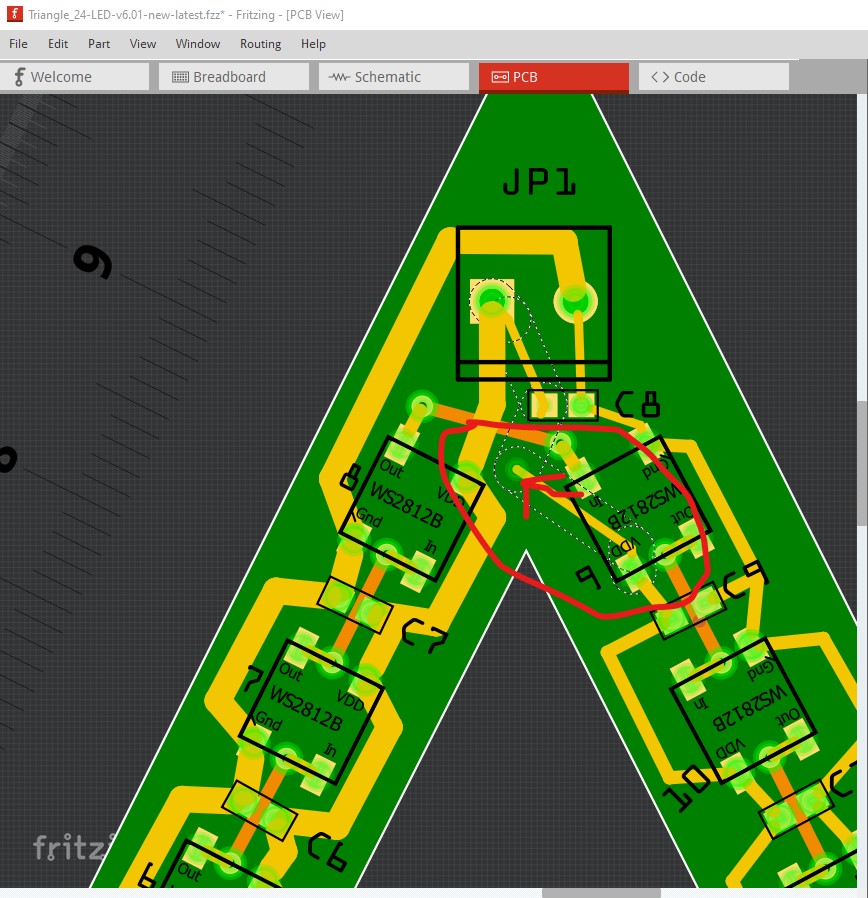
Delete this trace (circled in red here) as it causes an internal loop in the VDD line. As we see that connection is redundant, because no rats nest line appears when it is deleted and routing remains complete indicating the deleted wire isn’t needed, but it would provide an alternate path and cause current flow which is undesirable.
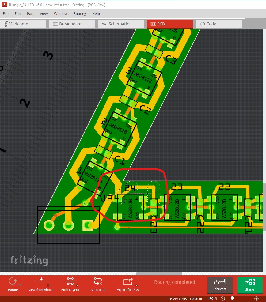
This wire is redundant (and causes a loop in the VDD path)

and thus was deleted without effect.
I am being anal about the trace size and routing because the neopixels draw a maximum of around 50ma (I thought this was higher the last time I looked at neopixels a few years ago!) per neopixel and thus 24 of them are drawing around 1.5 amps. That much current will cause voltage drop due to resistance in the traces. The bad effect of that is on ground. At the micro, ground is 0V and a low level signal is between 0v and 0.7v (the high between 2.4V and 3.3 or 5V is less concern!) Worse, ground at the micro is by definition 0V but by the time the ground from the micro gets to the neopixel (especially the later ones) if the resistance in the traces is even .1 ohm, “ground” which should be 0V the neopixel with potentially 1.5A running in the ground trace is going to be 0.15v higher than ground at the micro and it gets worse the further away from the micro the neopixel is. Thus a low level is now .15V closer to being a high level and if it gets too high, will stop working (or worse, sometimes not work!) because the micro can’t drive the signal low enough to be under 0.7V relative to the neopixel’s ground pin. I’m not sure how much of an issue that will be in this case, but the large trace sizes help keep that in check by reducing the trace resistance and thus the voltage rise due to resistive loss.
No, you don’t need a capacitor for LED 24, you actually probably don’t need most of the capacitors, but they cost nothing to include on the board and if you turn out to need them, they can be added without having to redo the board. I would start by only installing capacitors in the locations circled in green here, that should be sufficient bypassing. If it isn’t (indicated by things not working sometimes due to noise problems!) you can add more capacitors later, but it probably won’t be necessary.
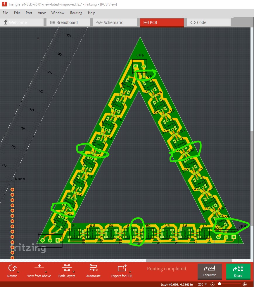
this puts a bypass cap near to each of the connectors then in the middle of each arm of the triangle.
Assuming the jumpers are the connectors, on the board, they will be a hole suitable for connecting to a wire (or installing the connector if you want to make the connection removable) and thus should be fine as is. If you want to attach a wire you can just solder it on to the pad. It looks to me like you should be pretty much ready to go now. One issue to think about is that the thick traces on the power pins may make the LEDs a little hard to solder (assuming hand soldering) as there is a lot of copper there to heat. You may want to try test soldering a neopixel to a 48mil trace on a test board to see how hard that will be. You can probably cut a scrap piece of copper clad to make a test case at little cost (other than using up a neopixel.) Just a strip of copper 48mil wide by a an inch or so long to avoid finding that you can’t solder them after buying boards. Other than that I think you should be ready to go. Here is the modified sketch that the above came from:
Triangle_24-LED-v6.01-new-latest-improved.fzz (90.0 KB)
Peter
Instead of removing the traces that Peter did, I would want to do the same but as far as possible from wherever you plan to connect power and ground to the PCB. That way, there will be less length, and fewer neopixels for the voltage drop to build up. It will also halve the «maximum» current through the traces closest to that connection point.
Good point! I hadn’t thought of that.
Peter
I’m thinking near the first led is where I would start the power in.
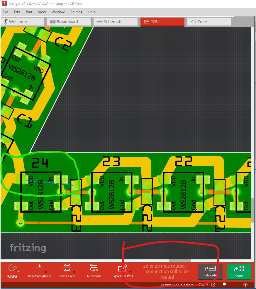
I’ve put all of the tracings for the power and ground to 48 mil. DRC checks out fine. The schematic for some reason has a problem with C10.
Triangle_24-LED-v7.01.fzz (84.0 KB)
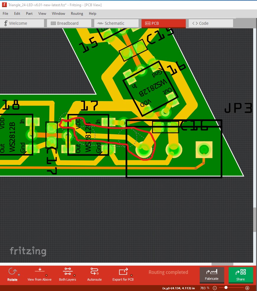
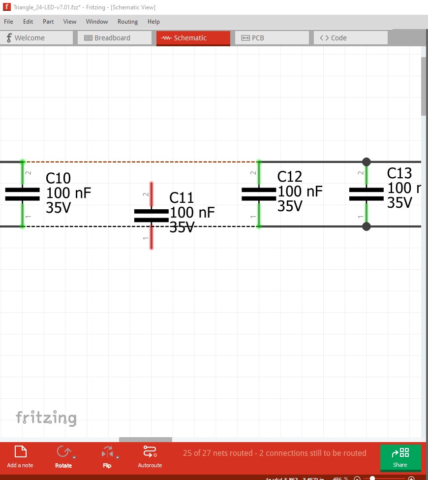
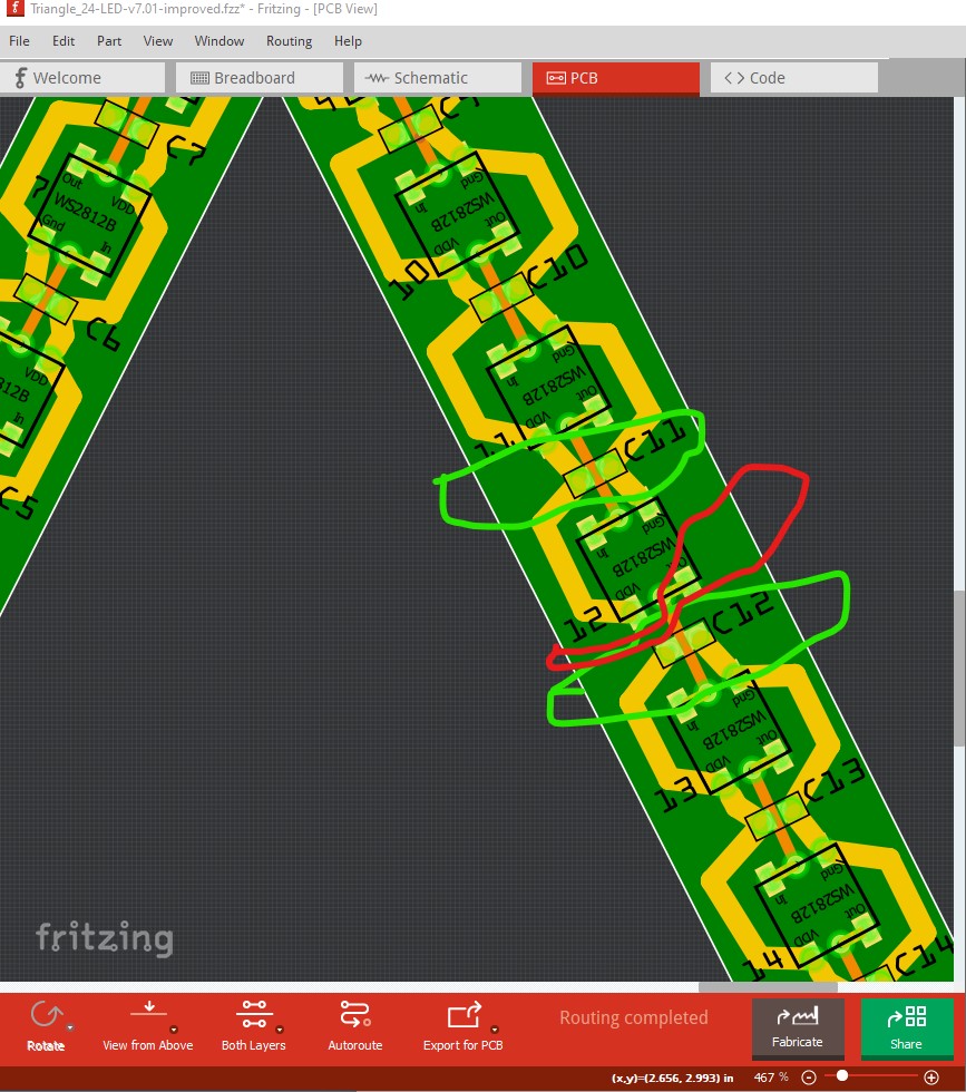
Interesting! This seems to maybe be the start of the routing corruption bug that hasn’t yet gotten too far. C11 needs to be flipped vertical so the wires line up, but while the routing database appears correct (because the yellow connected pins are correct) the line from C11 is going to the wrong place (circled in red here, it should be taking the green path) but for now that is only happening in the render of the lines in schematic and hasn’t yet effected the routing database.
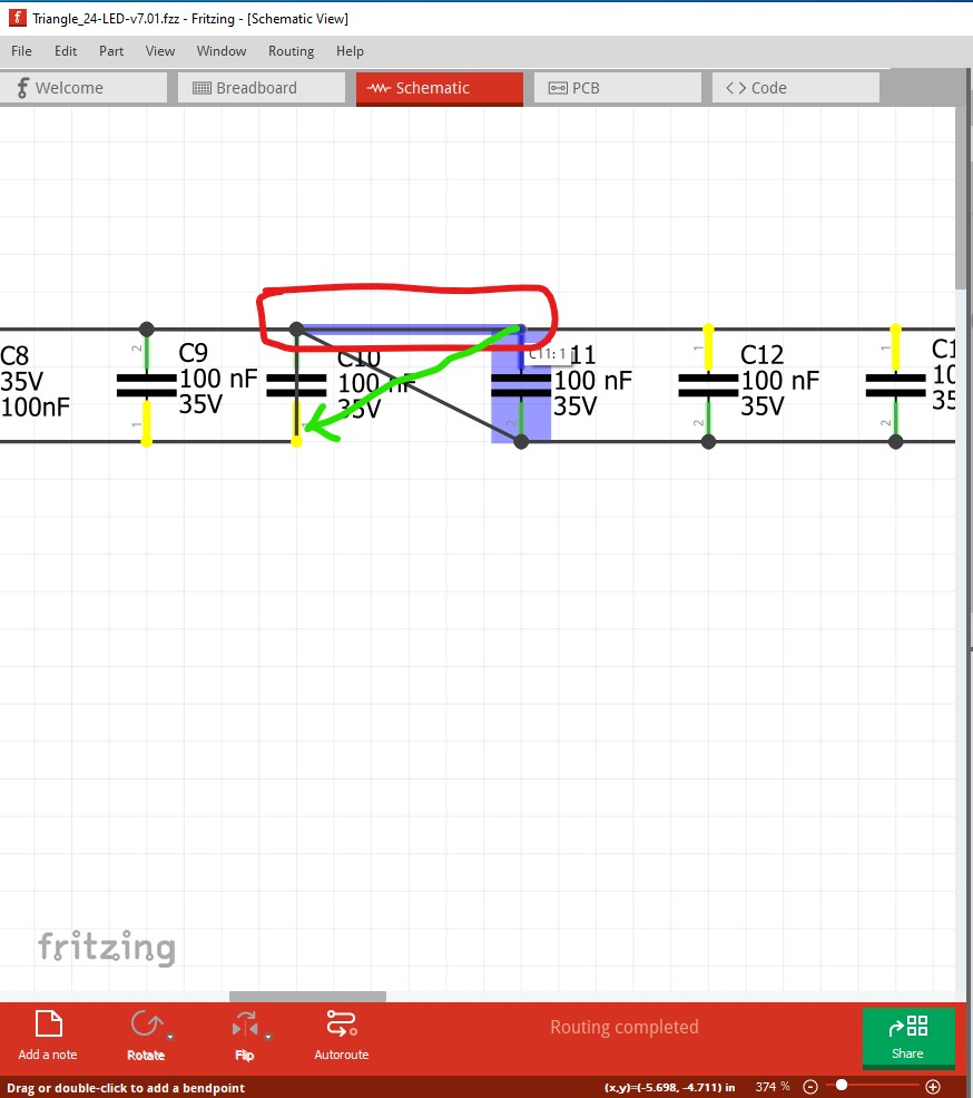
this should look llike this:
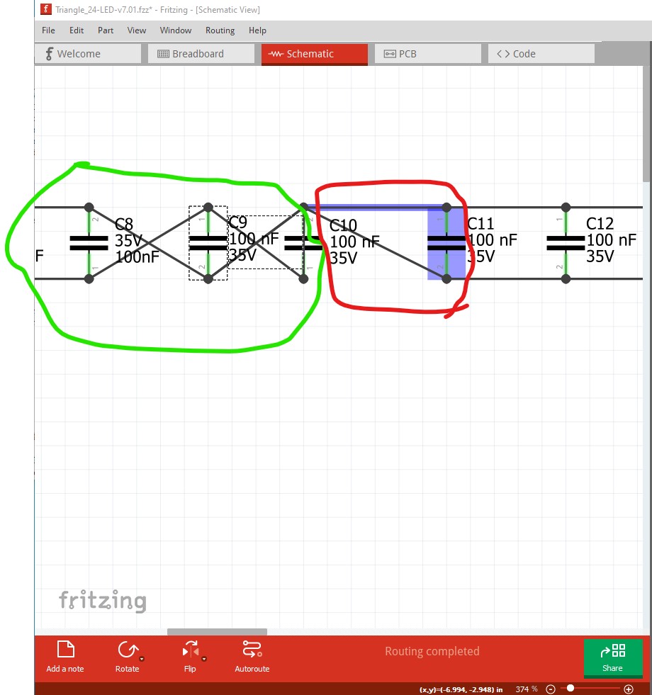
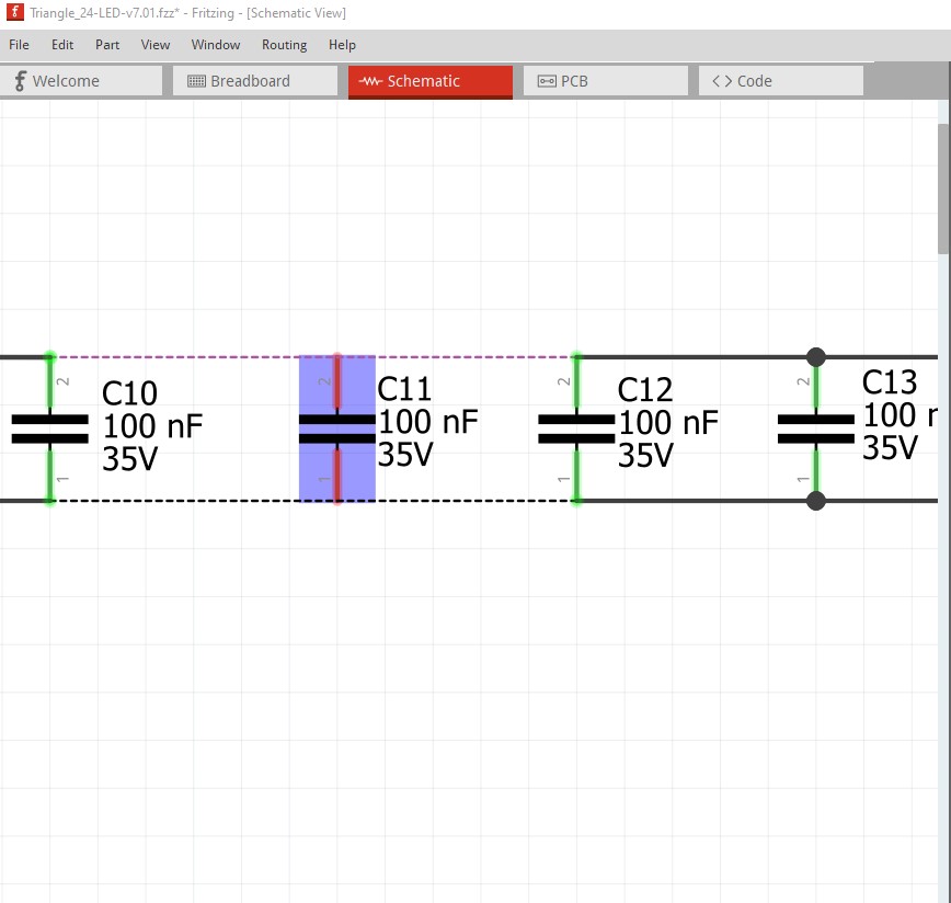
here I flipped vertical c9 and as expected both sides show crossed wires which is what c10 should be showing but isn’t. As noted the routing database at this point is still correct because the net connections are still correct. It is however very possible that this is what eventually leads to the routing database getting corrupted possibly because something follows the visual render path to get somewhere (incorrect in this case) instead of the net path. I can fix this by deleting the wires to c10 in schematic and then in pcb and re attaching them in pcb. That makes c10 in schematic react correctly again (it appears to be able to delete the wire in error still, I expect it eventually gets confused and can’t delete the wires!) We likely need to poke at this .fz file and see if we can figure out how it came to be this way. I started deleting wires in pcb to isolate c11, with it isolated completely there is a rats nest wire missing:

there isn’t a connection to the continuation of VDD as a rats nest line (although that connection still shows in schematic:

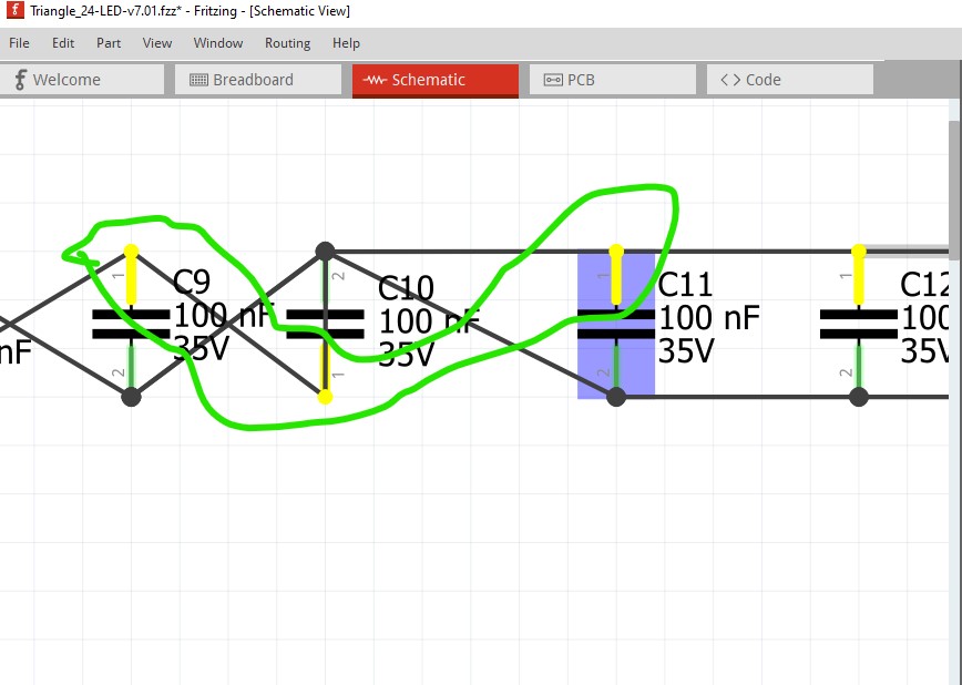
the routing data base still thinks the two nets are continuous (which come to think of it may be because we have a loop somewhere which is making the net still complete! Something else to look for …) This may be a valuable find if it helps find the routing database corruption! Moving back to schematic, deleting the wire to c11 has an interesting effect:
wire to the wrong place, no rats nest lines. Delete that wire and voila a correctly routed rats nest line:

And I expect if I route c11 in pcb again all will be well in schematic. Ah! mystery solved. The rats nest line is showing up, just not where I expected it (undoubtedly this is a shorter route by some criteria!) It appears on the path I removed on LED 24:
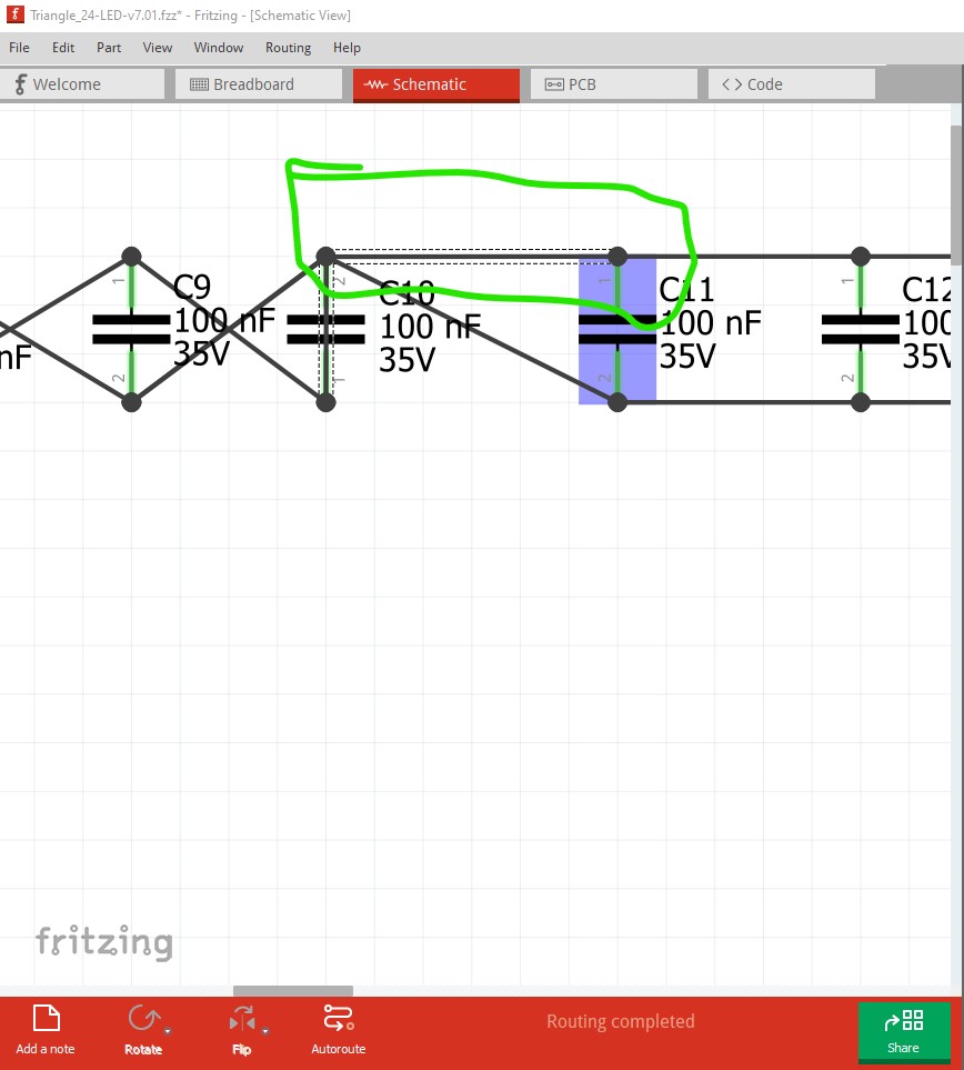
rerouting the connection to c11 indeed completes the routing as expected and I expect will have fixed schematic.
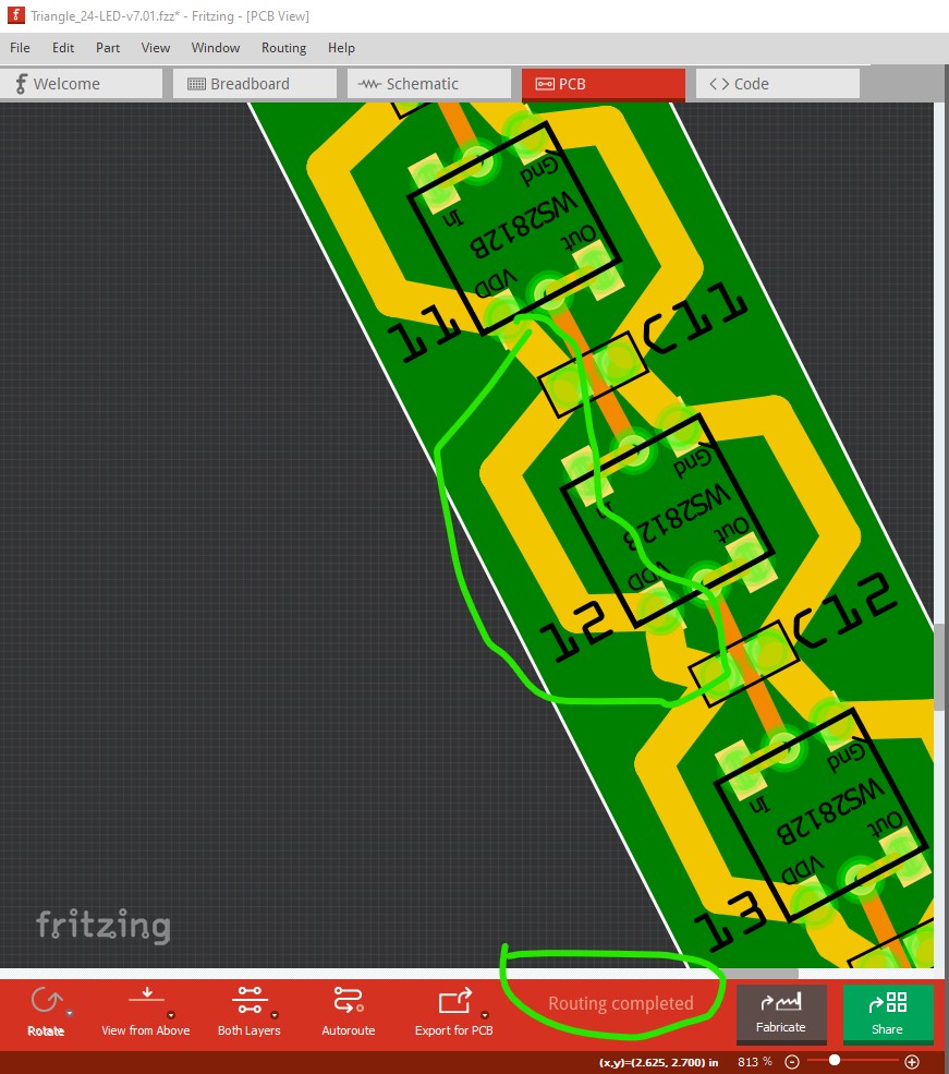
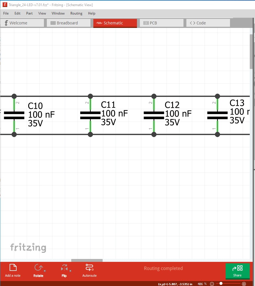
and indeed it seems to have. Now if I run down the line of capacitors and flip them vertical schematic should settle out correctly.
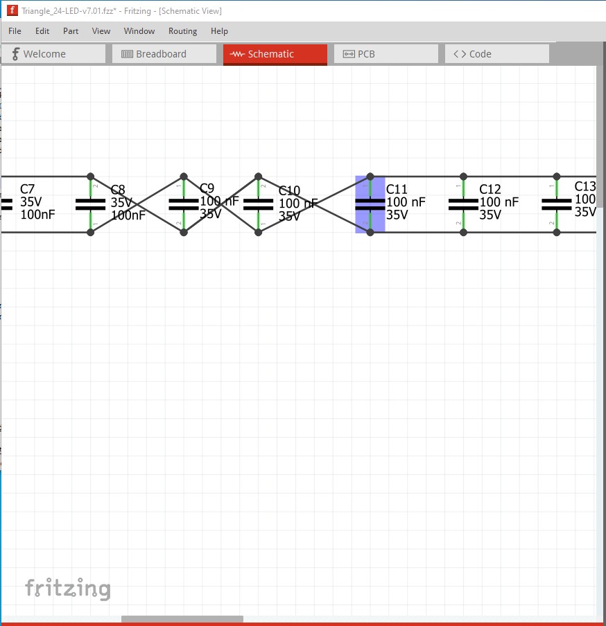
which is true except c11 is still unhappy about something. For some reason it is outlined in blue (which I haven’t seen before)
completely isolating c11 in pcb seems to work:

it is completely clear in schematic:
lets see what happens when we rewire it in pcb from this state.
so far so good, pcb is fine (as always) and schematic has the correct rats nest lines ready to be routed and no blue box. (so far )

and it appears successful this time. It will be interesting to figure out what the blue box is trying to tell us I expect.
I then finished the routing on the bypass caps (and moved c23 to the chain of caps) so schematic is complete in this sketch
Triangle_24-LED-v6.01-new-latest-improved.fzz (90.0 KB)
Edit: a late addition, assuming this is how you intend to power it:
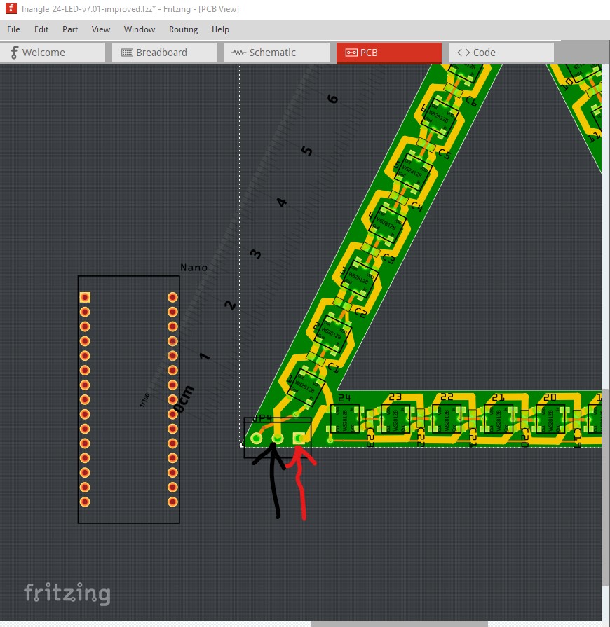
where the red and black arrows are the power input, then this power separation makes the most sense:
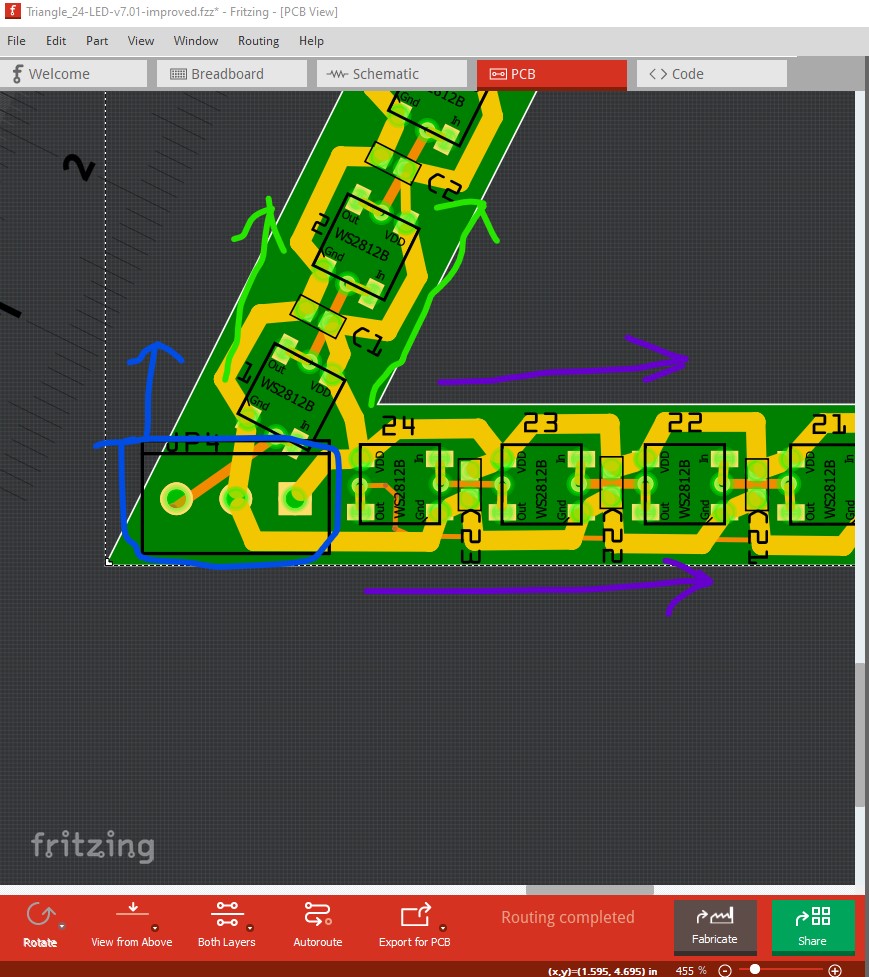
here i moved the connector up a bit to get room, then split power and ground in to two legs the green leg up the triangle and the purple leg across the bottom. They meet (and disconnect) in the middle of the third leg putting approximately the same number of leds in each leg.
Here is the new disconnect point (at our friend c11 by coincidence!) Here you want to populate both c11 (last cap on the green leg) and c12 (last cap on the purple leg. This splits the current in ground in half (halving the effect of trace voltage drop as well as reducing the current by 50% due to two paths which helps even more!)
(forgot to include the sketch!)
Triangle_24-LED-v7.01-better-power.fzz (89.0 KB)
Peter
1 Like
I just realized that because of how neopixels work, the logic level ground creep isn’t an issue. Because the signal is regenerated on the neopixel, the relevant ground is the neopixel that is driving the current neopixel. Since it is only about 1/2in away, there will be basically no ground drop since the ground is only 1/2in long. It is still a good bet to use the large traces though to avoid power issues.
Peter
1 Like
@vanepp Peter, do you think this ready for fabricating?
It looks so to me, as long as it meets your needs I think it should be ready to go. I just output the gerbers and they look fine to me.
Peter
1 Like
I’ve sent it to be fabricated. I’ll see what happens.
Thanks for all of the help. Learn a lot.
Scott