Raspio Triangle Request

Not quite ‘in’ screen space, but your symptoms indicated that it it is probably being translated ‘through’ the associated screen coordinate system. As a guess, coordinates entered into Inspector are converted to a (rounded and truncated) screen pixel coordinate, which is then translated back to physical units, which are what gets stored. The second part is what HAS to happen when positioning a part by dragging it. When positioned by coordinate value though, that just reduces the accuracy/resolution.

Since we have seen no indication of the coordinates changing (after setting and being ‘messed up’) when zooming out and back in, once they are ‘saved’ to the sketch, the translation is all one way. Picking the ‘best’ screen coordinate to display something based on the previously stored values. So what is needed, is for Inspector to ignore the screen, and store the entered (and scaled based on only the sketch units) values, then have the display code read that for its processing to graphically position the part. Just as it would do for a part that had been positioned previously at a different zoom level.

Another ‘trick’ would be to have Inspector work with a ‘virtual’ zoom level. So that its calculations are always working from a maximum zoomed in screen. I found in that past that Fritzing does something similar for DRC. Design Rules Check processing renders traces and connectors associated with a net list to a temporary internal image. It expands that by the keepout setting distance, then does a boolean ‘and’ operation with other (non expanded) rendered net list (and edge) images to detect overlaps. If that ‘anded’ image is not empty, something overlapped. Same for autorouting. It graphically (in pixels) tries to ‘connect the dots’, turning aside when it encounters existing copper.

1 Like

Sorry I caused such a controversy on these coordinates.

I have worked my way thru a new version, with the WS2812b. Attached is a so far file. I need to get a the holes for 5V, GND, DIn and DOut placed around the triangle.
Triangle_24-LED-v1.5_ws2812b.fzz (15.8 KB)

It caused us to figure out a work around to the issue, so it was a useful discussion (and it may cause a proper fix to be considered :slight_smile: .) The spacing looks good, I think I would move the LEDs closer to the middle of the board like this so the bottom power trace can be increased in width as it is likely to have a fair amount of current.

I would center the LEDs in the board space to leave as much space for the power traces as possible like this:

Here I set the grid size down to 0.025in and increased the trace size to 60mil by typing 60 in to the trace size window in Inspector with the trace selected. I would also suggest putting bypass caps across the power traces every 3 or 4 leds to reduce spikes on the power lines. To avoid voltage drop you want the power traces as wide as possible. Another point to consider on neopixels is that you need to plan the power supply to be able to supply the maximum current that the entire set of neopixels can draw in the worst case. That is because the WS2812b are asynchronous clocked by rc oscillators on chip and thus will sometimes all get in sync and draw maximum current. If your power supply current limits at less than the maximum current the LEDs can draw, VCC will drop and the LEDs and/or the micro may hang. Other than that it is looking fairly good. I think some of the grounds may be isolated and there need to be connectors (I would use 0.1in headers I think) to connect to the micro, but other than that it is looking good!

Peter

1 Like

That’s not a problem. It’s when people try to push the limits that we see where the limits are.

Something that can help later: Once the parts are positioned correctly on the pcb “lock” them and the PCB itself into position. That keeps them from accidentally being dragged while working with the traces. On the Edit menu, Select All, then on the Part Menu, Lock Part. Individual (or groups of) parts can be selected, and the lock toggle in Inspector as well. Locking can be done separately on each view.

The positions of the LEDs on PCB view for the left and right diagonal arms of the PCB are not quite symmetrical. It looks further off than accounted for by the ‘glitchy’ coordinate rounding.

Looking at the ratsnest wires on PCB view, it is difficult to tell exactly where the connections are. Wires are drawn on top of each other, making end points difficult to determine. To ‘fix’ that, I ran autorouting. Normally I do not recommend that. It tends to do a poor job. But the circuit here seems simple enough for it to give usable results. Autorouting did not finish all the traces, but it is enough to look at the connections. I let it run 500 cycles. Since this is a regular series of parts, the connections should form a simple pattern. All of the “Gnd” pins tied together, all of the “VDD” pins tied together, and each “Out” tied to the “In” of the next LED. That is not what I got. Inspection shows there are wiring errors. Here are some of them.
LED 1 Gnd is not connected
LED 2 Out is connected to Gnd
LED 3 In is connected to Gnd


Your attempt to minimize (and overlap) the spacing in breadboard view is the likely cause. Some of the wires there are not going where they visually appear to be. It looks like you are trying to make the breadboard view align with the physical position on the pcb. For something like this, the breadboard view could (maybe should) be spread out a bit more, so that the wiring can be seen. Personally, I would start by wiring the schematic view. Then use the generated ratsnest wires to route wires on the other views.

After deleting all wires in all views, I adjusted the schematic view and routed it. I then ran autoroute on PCB view again. It got a little further, but still did not complete. The pattern is more consistent this time. There are some obvious bad choices that prevent the data lines on the right arm from completing. To simplify the routing, I was considering a ground trace on the bottom, with vias connecting to the top beside each led gnd pin. In general, minimizing vias is a good idea. Not needed for the bottom, but should clean up the left and right side data traces a lot. You could also consider rotating the left and right arm LEDs by 180 degrees to get the in and out pins adjacent, like the bottom. Other things Peter mentioned apply.


My partial version (schematic and autoroute pcb).
Triangle_24-LED-v1.5_ws2812b-1.fzz (40.0 KB)

Here is a version with each of the side arm leds rotated 180 degrees, with all of the leds shifted toward the centre of the triangle enough to allow traces between the leds and the outer edge of the pcb. See how clean the trace pattern is now. No vias. It is single sided. This is not quite ‘ready to use’ yet. Each of the arms of leds was moved as a group, but that was done by eye. The led positions should be adjusted to be as mathematically precise as Fritzing will allow. Also, the traces could be cleaned up a bit. They were manually placed, with only a little effort to line up the spacing consistently. Also, from what I see in some youtube tutorials, ‘best practice’ is to have the traces meet the pads square on, instead of at the about 45° that most of these are. See the second image for an example. The power and ground traces could be make thicker as well.

Triangle_24-LED-v1.5_ws2812b-2.fzz (42.1 KB)


I would suggest adding pads (you don’t necessarily need to add the caps!) for a tantalum cap at each LED. The pads are free even if you don’t populate them (and can take 0.1uf ceramic caps as well as tantalum) and can (and probably should!) be mounted on the bottom of the board to avoid interfering with the view of the LED. That way if you need the caps due to power problems you can add them. To get the caps in and to pass DRC I needed to sat the grid size to 0.125in and I boosted the trace size to 48mil. If the caps are mounted on the bottom of the board they won’t interfere with the sight lines to the LEDs (and don’t need to be added if they aren’t needed!)

With the Nano moved from the center of the triangle default DRC passes.

The cap needs to be increased to 0.2in pitch in Inspector to get enough room to route the traces. All the power traces should be 48mil (I only did three as an example!) Here is the sketch this was taken from.

Triangle_24-LED-v1.5_ws2812b-3.fzz (45.3 KB)

Peter

1 Like

Thanks for the hint. I think I found the cause of the problem. I wrote my thoughts in the bug report: Placement is imprecise / rounds input · Issue #3639 · fritzing/fritzing-app · GitHub

Unfortunately, I am quite busy and I do not time to fix it now, but hopefully, someone will do it soon.

Where do I find the 5V and GND symbols that are used in this image?

Also, in regards to capacitors, I need one between each led? I can’t quite make out the size of the capacitor in the image. I see it is 200 mil and 35v.

Thanks

You probably don’t need one for every LED, but if you add the pads when making the board you have the option of putting in as many as you need. It is 200mil because 100mil makes the pads too close to the LED to run the In to OUT trace between the pads, the actual caps are likely 100mil so you would have to bend the leads a bit. I left the size and voltage at the default, in practice 15V caps should be good (6V caps in a 5V system doesn’t leave enough head room for my taste although it should work!) You can also use ceramic caps in place of the tantalum ones if you like, but setting up for polarized caps (where the direction matters!) is safest.

Peter

1 Like

Playing, I did a variation on Peter’s optional capacitor placement. I increased the spacing to 300mil, and added a second smd capacitor in parallel. Both on the bottom on the board. That way either THT or SMD parts can be used. The THT would need to have the leads bent to reach. You would not want to really use 300mil electrolytic capacitors here. 0405 SMD parts fit nicely between the holes for the THT cap. Positioning is fairly tight, to keep the THT holes and pads from either getting too close to the PCB edge, or interfering with the LED on the other side, while also keeping good angles for the power traces bends. I wanted the THT holes to be at the bends in the traces.


For size, as Peter says, the standard 6.3V caps are not really enough in a 5V circuit. 10V or 16V caps would be safer. For the capacitor value, since this is intended for filtering, bigger tends to be better. Within limits. Too much will make the power supply work extra hard charging them when power is first turned on. What is needed depends on how good the power supply is, and resistance losses in the traces. Something that can easily handle the maximum load of the full circuit might not need any at all. If the power supply is a bit lighter, or switching an LED from off to on can cause a momentary (local) voltage drop for the following LEDs, then adding filter capacitance can help keep it stable. There are trade offs. One larger capacitor at each corner of the triangle can be approximately equivalent to a smaller capacitor at each LED.

Probably the most important place to add filtering, is at the Arduino board. The circuit “may” work fine without filtering for the LEDs, but voltage drops at the microcontroller can cause resets and other problems.

If you know you will only want to use SMD parts, then the THT capacitor can be replaced with vias at the bend points. vias are smaller, and will not interfere with the LED. Keeping shallower bend angles on the power traces is easier. I would increase the via ring thickness to match the trace size though. If it fits, maybe just a little larger, to compensate for the hole itself. You do not want the hole size too small. That is the ‘trace’ to the other side of the board. Technically that trace ‘width’ is pi * hole diameter (the hole circumference).

1 Like

Since I was playing with rotated capacitors, how about this? Rotate the SMD LEDs to make alignment with the capacitors easier. This has the left arm LEDs rotated at -130°, the 300mil capacitor at -130°, and the 0405 capacitor at 50°. The row of LEDs on the left arm of the triangle have been shifted toward the centre of the triangle, so that the rotated 300mil capacitor has approximately the same clearance from the inside and outside of the triangle, and the traces from the LED pads to the capacitor THT connectors are (close to) perpendicular to the flat end of the pad.

Thinking outside of the pure rectangular box.

1 Like

I’d like to keep everything in the SMD format and have a smooth back if possible.

I’ve created a new version and performed the auto-routing, but what a mess I have. I will upload the file a bit later today.

Triangle_24-LED-v3.03_ws2812b.fzz (57.0 KB)

Yes it looks pretty messy! However here is a solution. First select our capacitor, (in this case, select what SMD case sizes we can get in Fritzing first!) I chose a ceramic cap in 0603. Then on digikey I set up to select all SMD tantalum caps between 10V and 25V in a 0603 case (to match the Fritzing footprint.)

The 22uf cap is a reasonable choice (most capacitance for a reasonable cost)

but there are lots of other choices. Now having our capacitor specified back to Fritizng and make some changes to your layout.

first the selected SMD capacitor is too large, the pads are too close to the LED pins and the physical capacitor won’t fit between the LEDs, thus the reduction to the 0603 footprint which solves both problems (the cap will physically fit between the LEDs and not fail DRC!) However the placement of the new cap means we can’t route the in to out LED traces on the top of the board. So place vias (circled in red below) and connect the vias on the bottom of the board (which leaves the bottom of the board flat as desired as the cap is on the top between the LEDs)

The vias will need to be placed and routed manually, I don’t see a way of doing this with autoroute, but it is easy enough to do if your are careful (the part overlaps make selecting parts hard once placed!) Here I did the first two LEDs (mostly, the vias need to be added to the second one!) Every LED has the pads for a capacitor but you don’t need to put a cap on every pad unless you need them (but if you do need them you have the place to put them!) Next there are DRC issues on your board:

Here I moved the various connectors (and the micro!) away from the boarders, but it still complains about something (but doesn’t select what!) that is too close to a boarder. The rest are the old capacitors overlapping the LEDs and that should clear with the new layout. Hope this helps!

edit:

Here is the sketch that created the above:

Triangle_24-LED-v3.03_ws2812b-fixed.fzz (32.0 KB)

Peter

1 Like

Triangle_24-LED-v5.02_ws2812b.fzz (39.6 KB)

Cleaned up some of the items, pointed the LED’s all in the same direction, forgot about the caps for now. Will start a new one with vias on the board.
DRC still has lots of errors. I’ll work away at it see what I can come up with.
Keep on playin’

Good progress! I have made even more (although this will be a little long :slight_smile: .) First about the DRC errors, they are all easy to correct (although there is a serious problem in the sketch!):

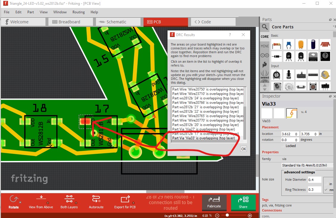
If you click on the line (as I have done here) and then zoom in on the connection it highlights, it will show you the conflict in red (possibly small and easy to miss!) move the line up a bit and the problem will go away.

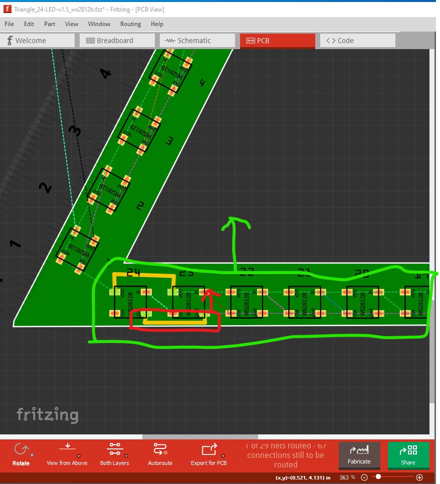
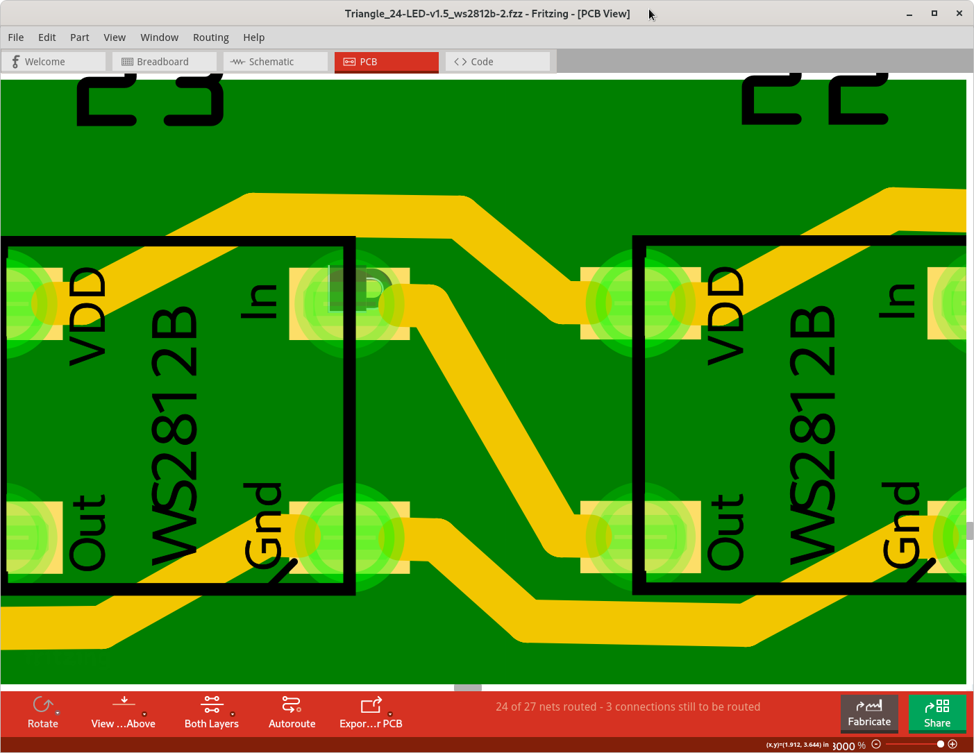
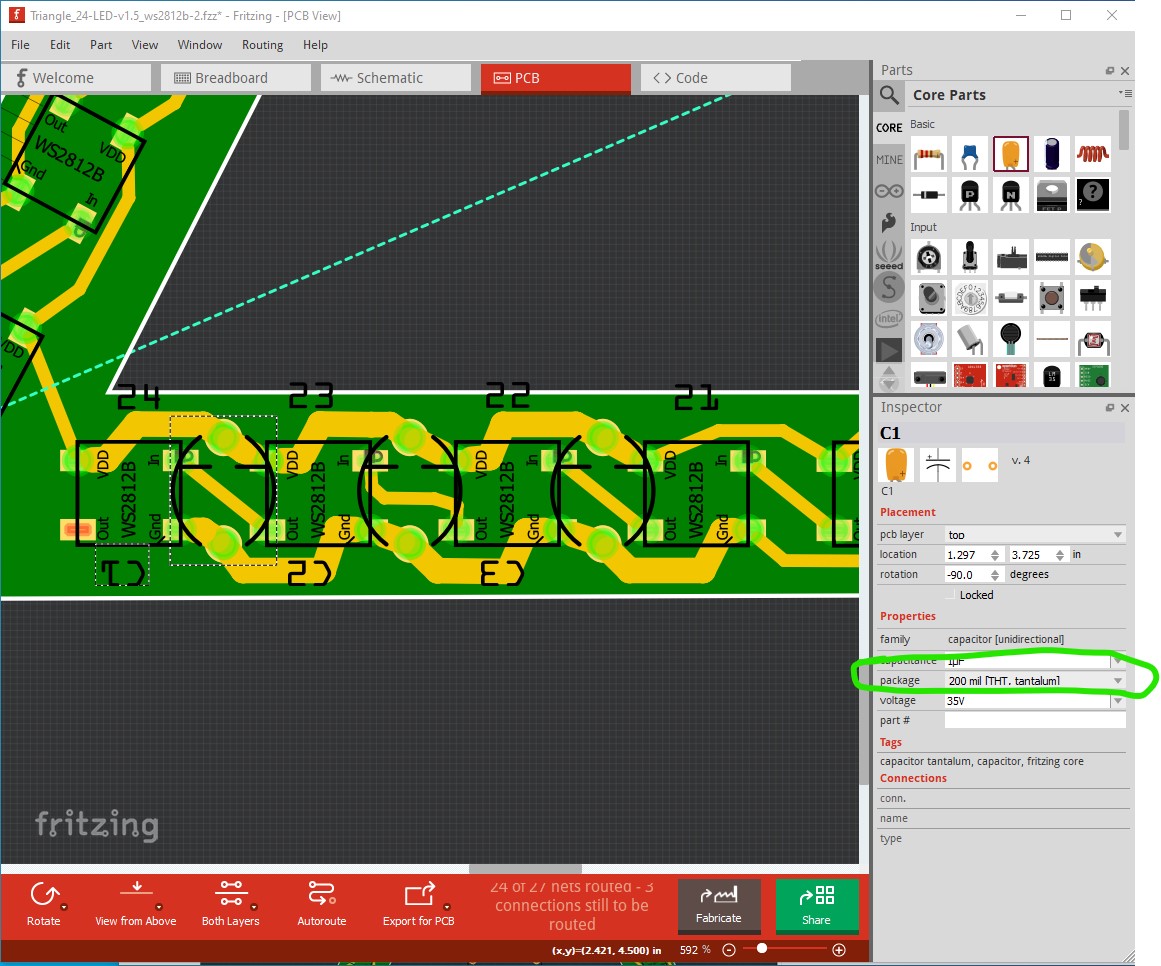
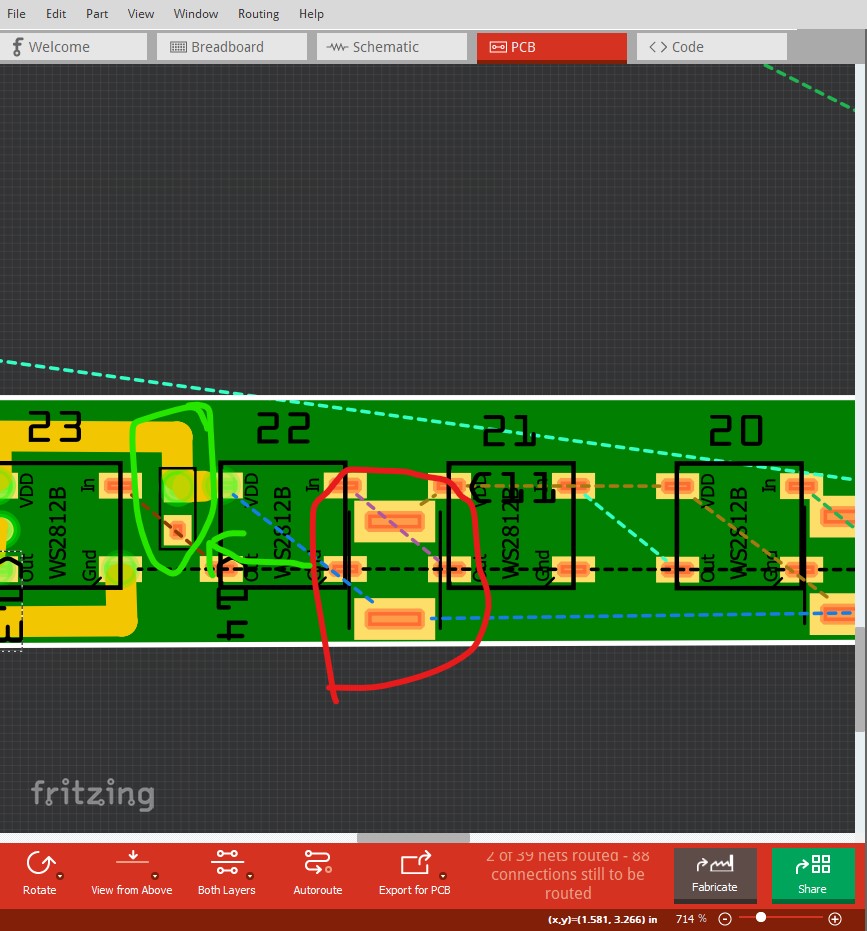
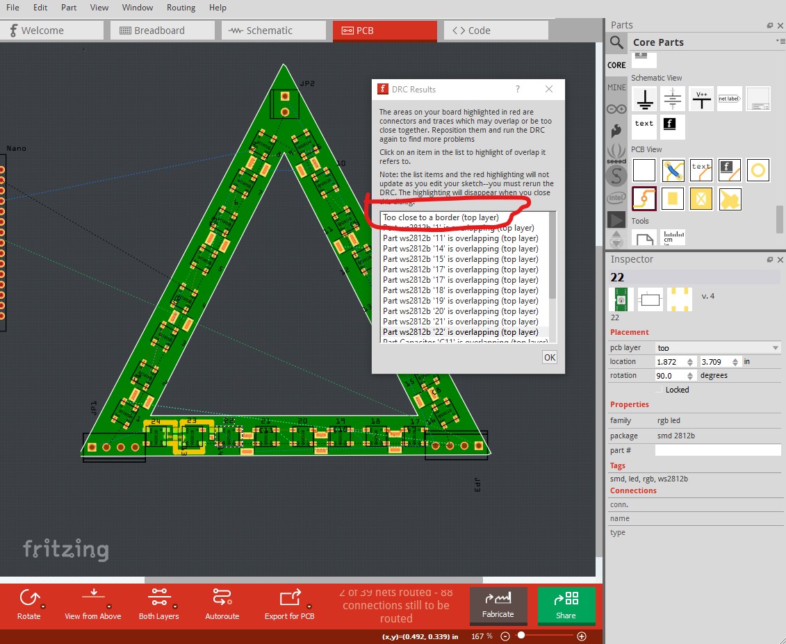
Same with this one. It is complaining about the trace circled in red being too close, moving the trace will clear it. The one circled in blue indicates a short on the top layer between VCC and GND (it will be reported somewhere else in the DRC listing as well!)

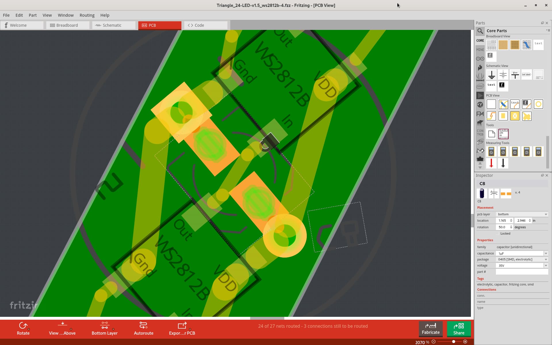
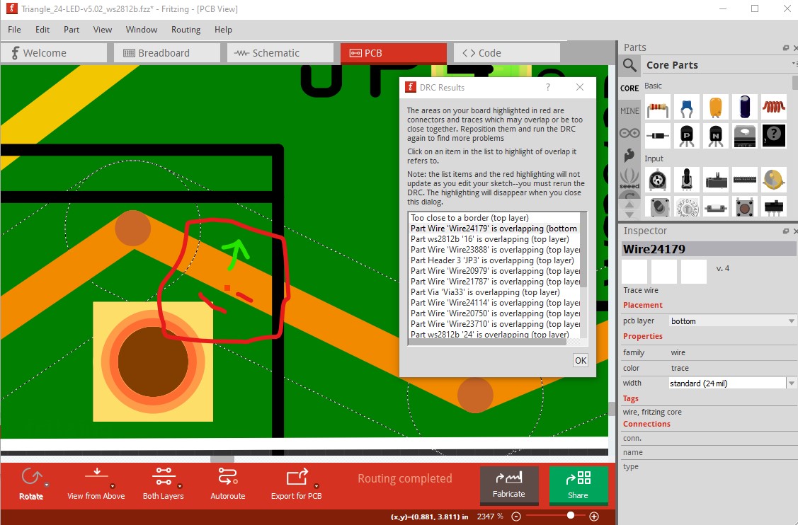
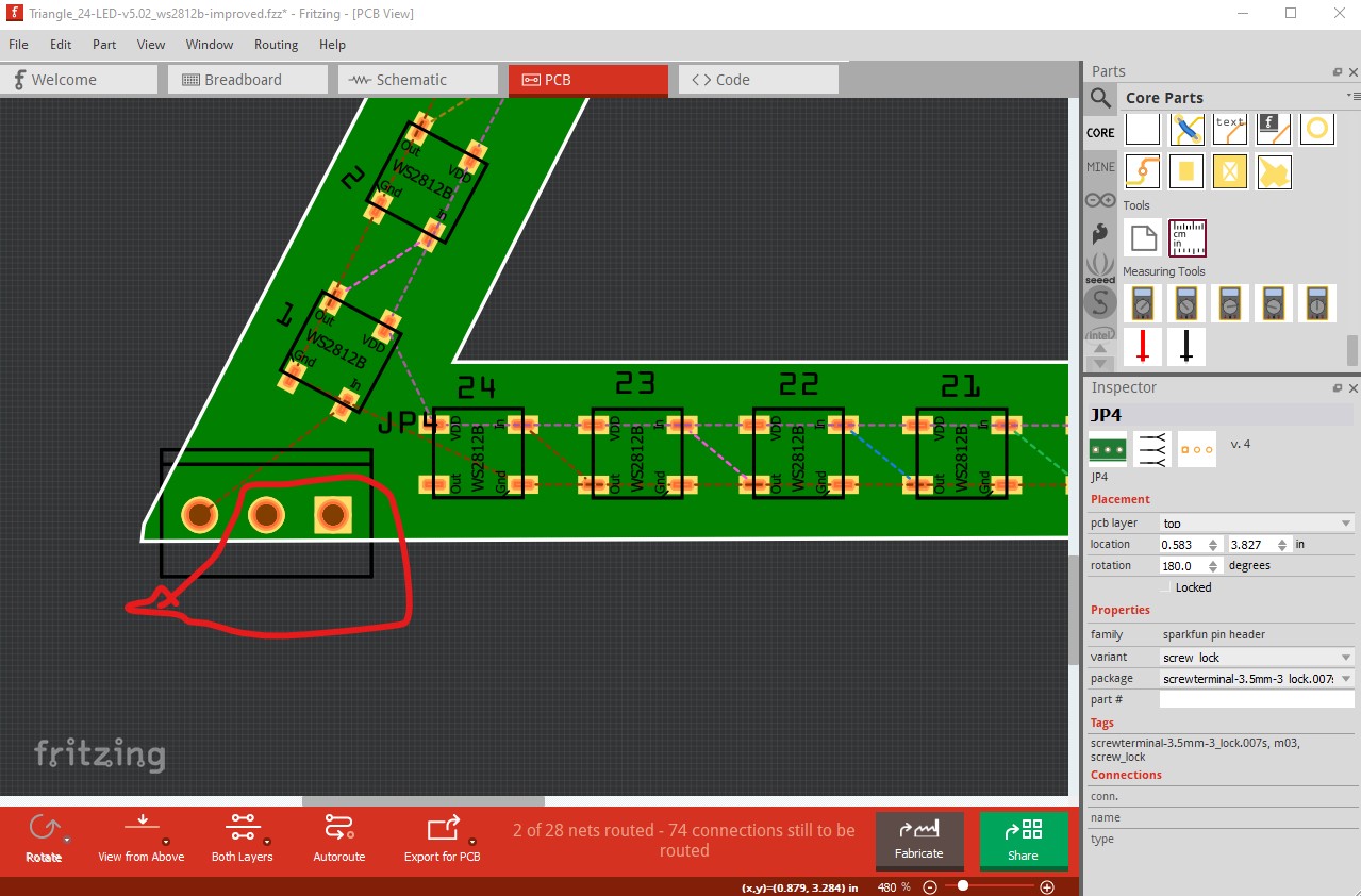
This one took me a while to find! The problem is there is a via hidden under the LED part. You can`t select it until you move the LED out of the way though (nor see it!) Here I moved the LED to show the offending via under it.

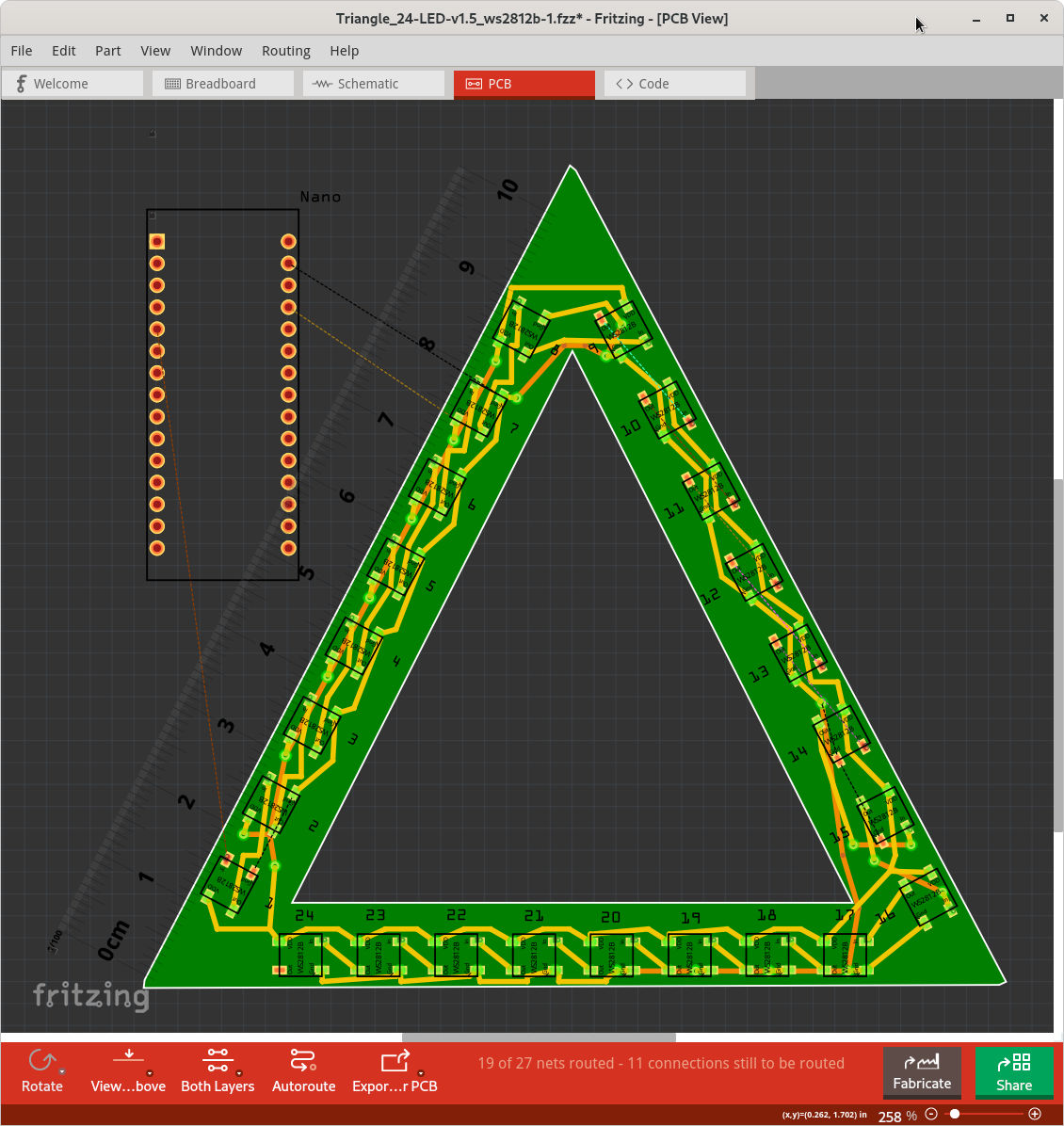
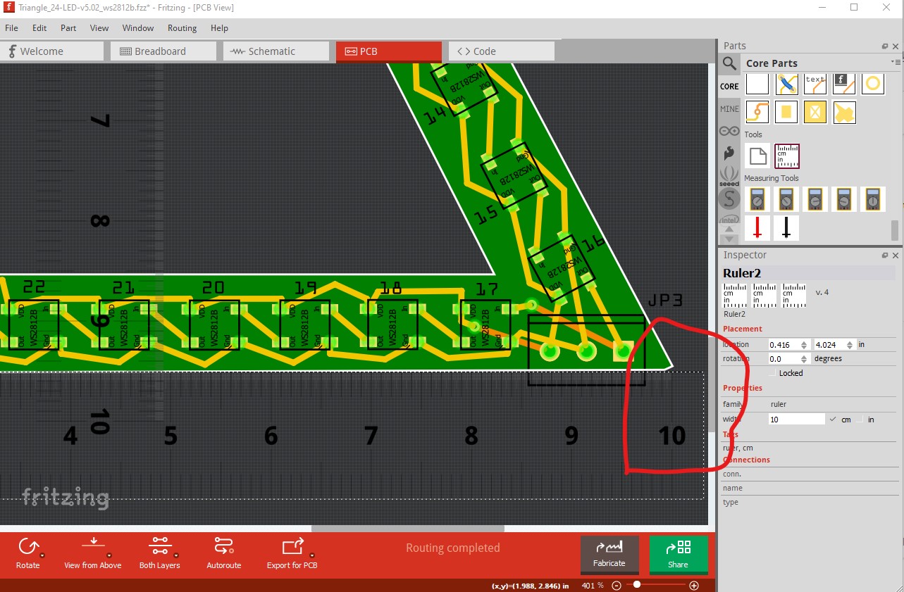
Now some layout questions (not necessarily errors, but they seem odd and may need addressing if you are not aware of them.) First the triangle is less tall ((about 9.7cm) than it is wide (almost 10cm) according to the rulers. I`d expect all three sides to be the same. Is this intended for some reason?

detail of the height difference.

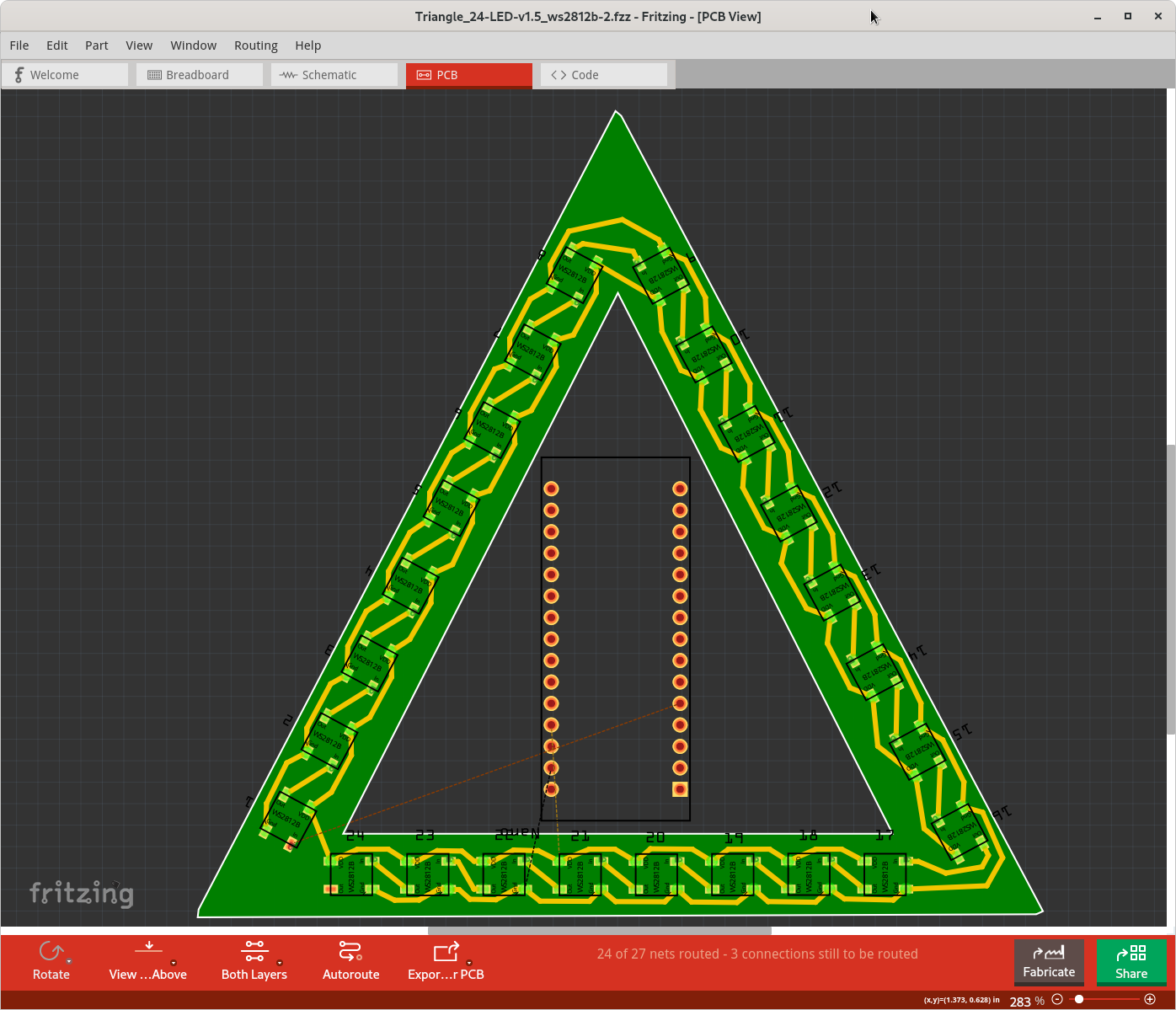
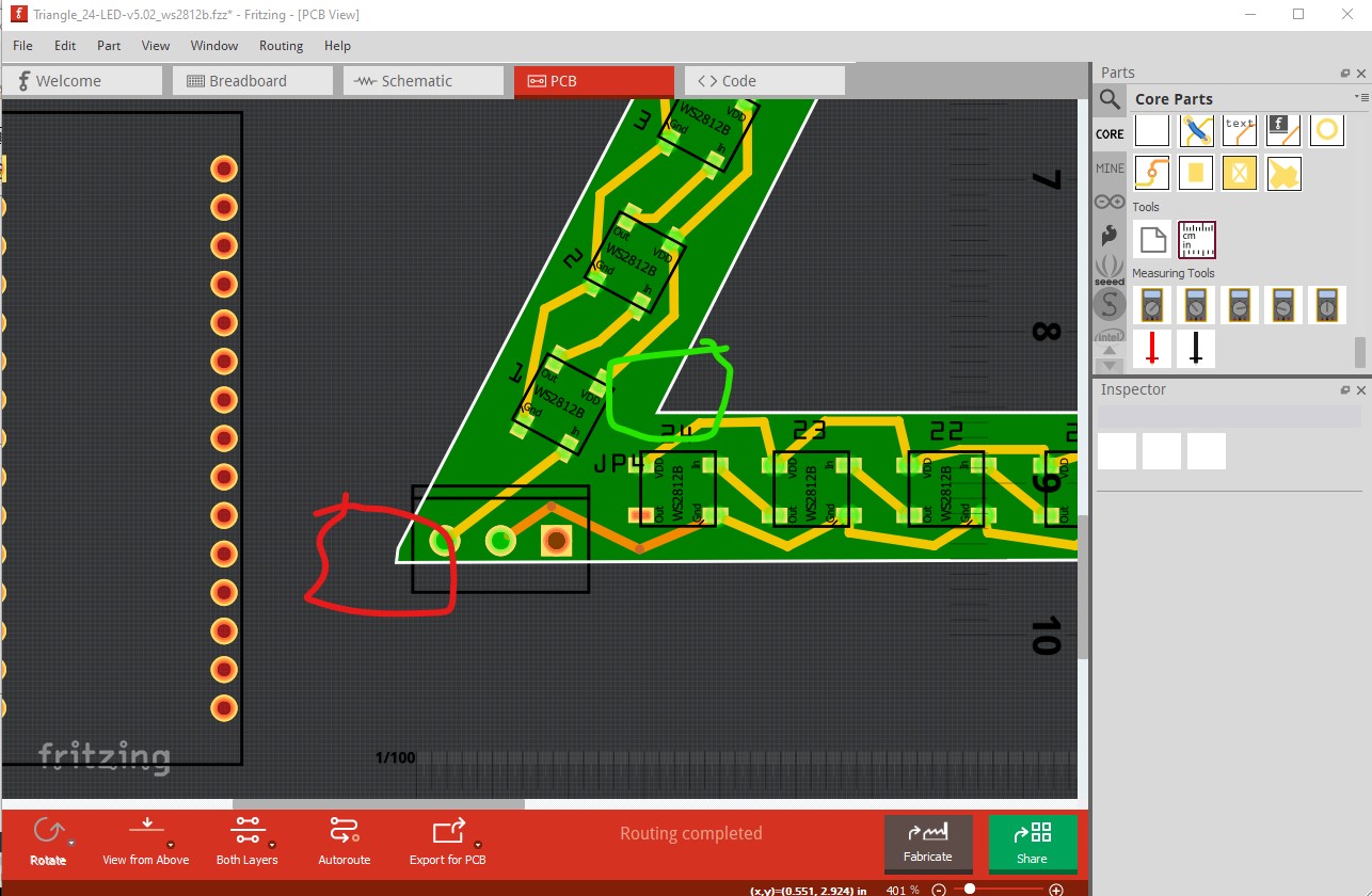
Next there look to be errors in the corners of the outline svg as shown here. The inner join (circled in green) is as I expect, the outer corner (circled in red) is misshapen. Is this intended? The board will be milled like that so the corner will be somewhat distorted I expect.

drc6

Perhaps the outline svg needs some adjustments in Inkscape to clean up the corners?

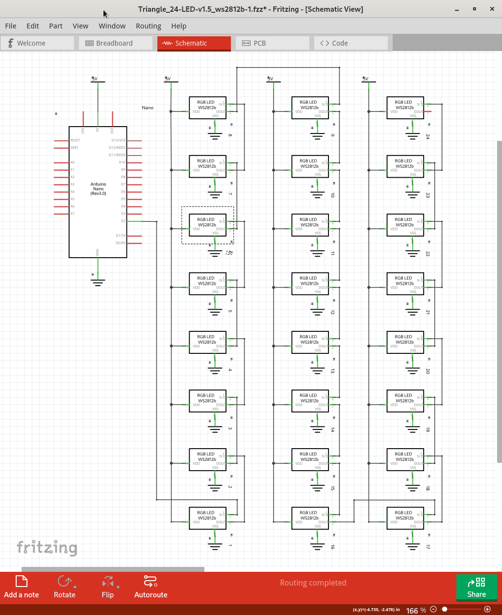
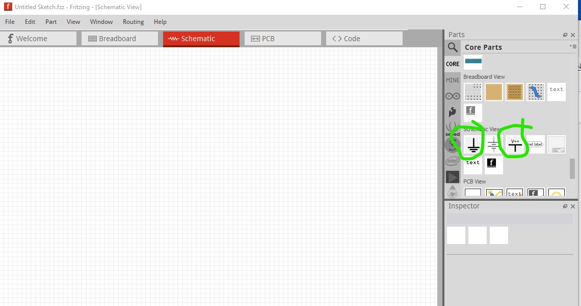
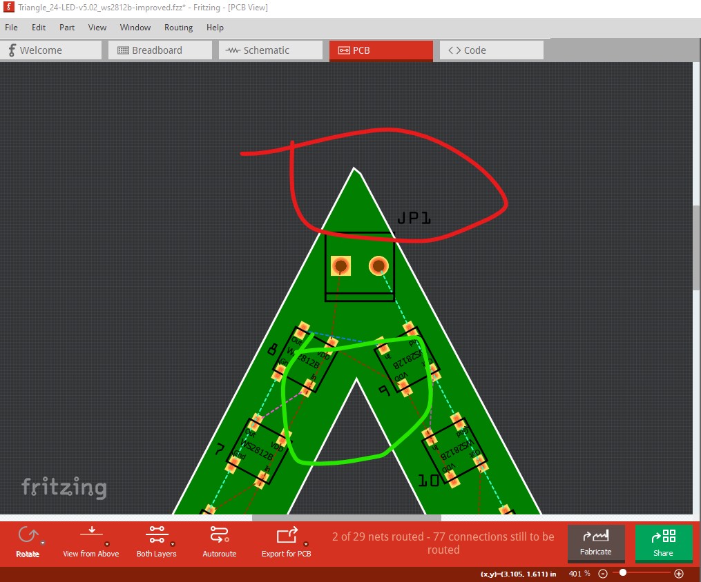
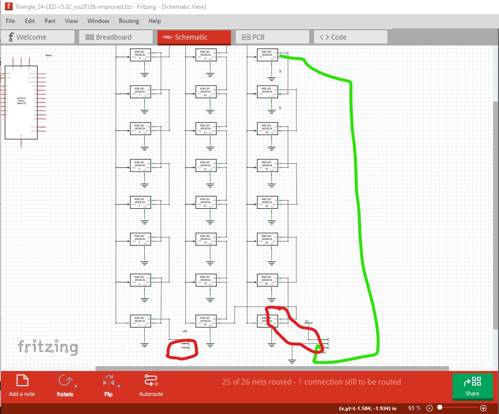
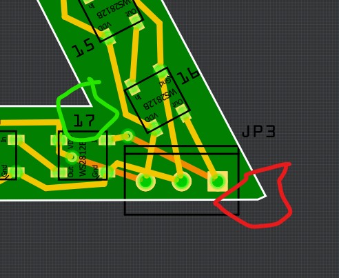
One pin on J4 has no connection. In the end by doing schematic I corrected this (you need to check that my correction is in fact what you want though! It may be that you wanted an output in the middle fot the LEDs for some reason, although it seems more likely an error!

This is what I think the error is in schematic. I think the last LED in the chain’s output should go to the header not the middle one as currently happens but there may be some reason for doing it the way it was connected.

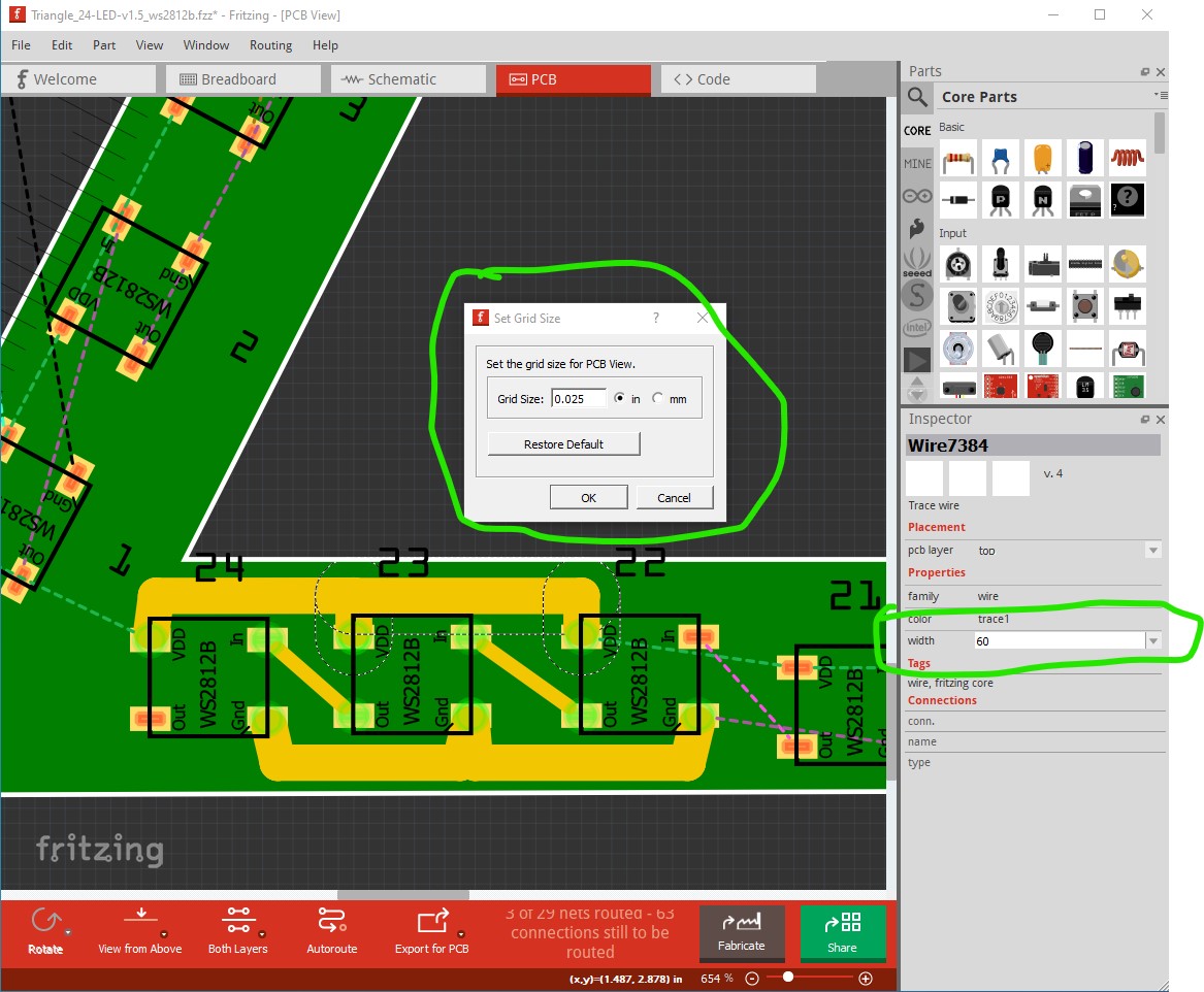
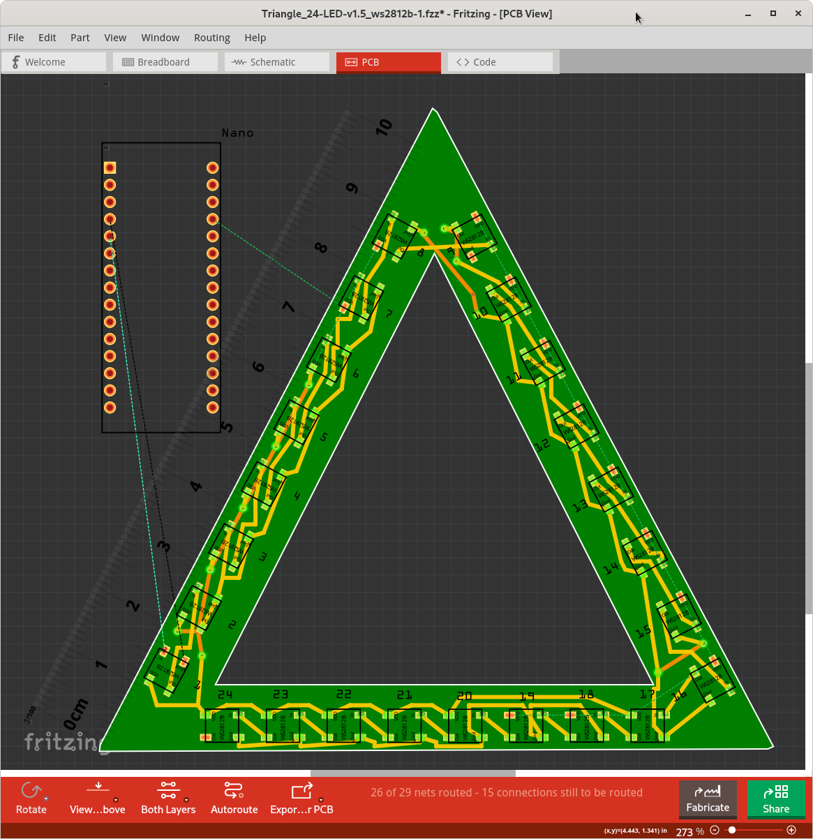
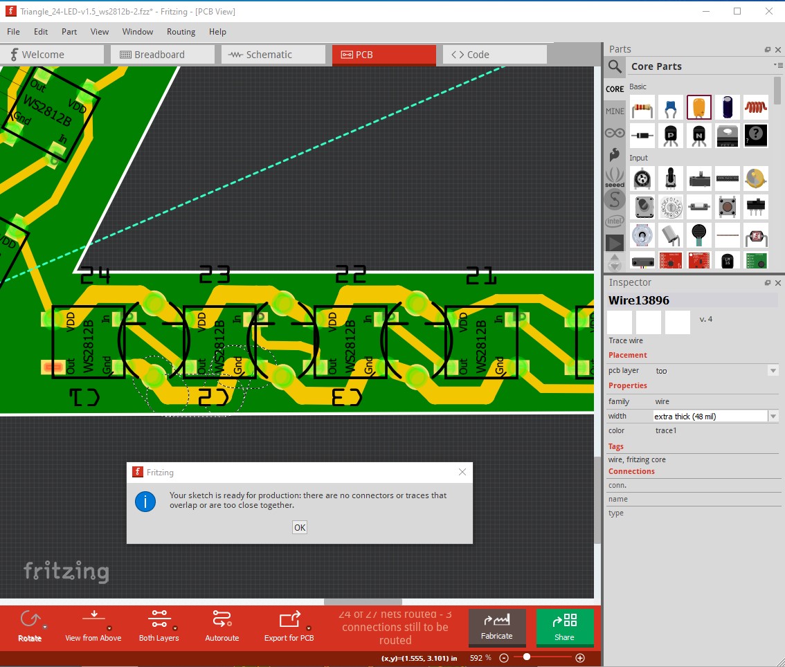
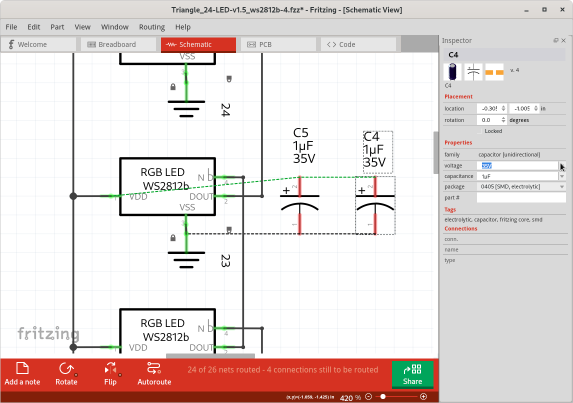
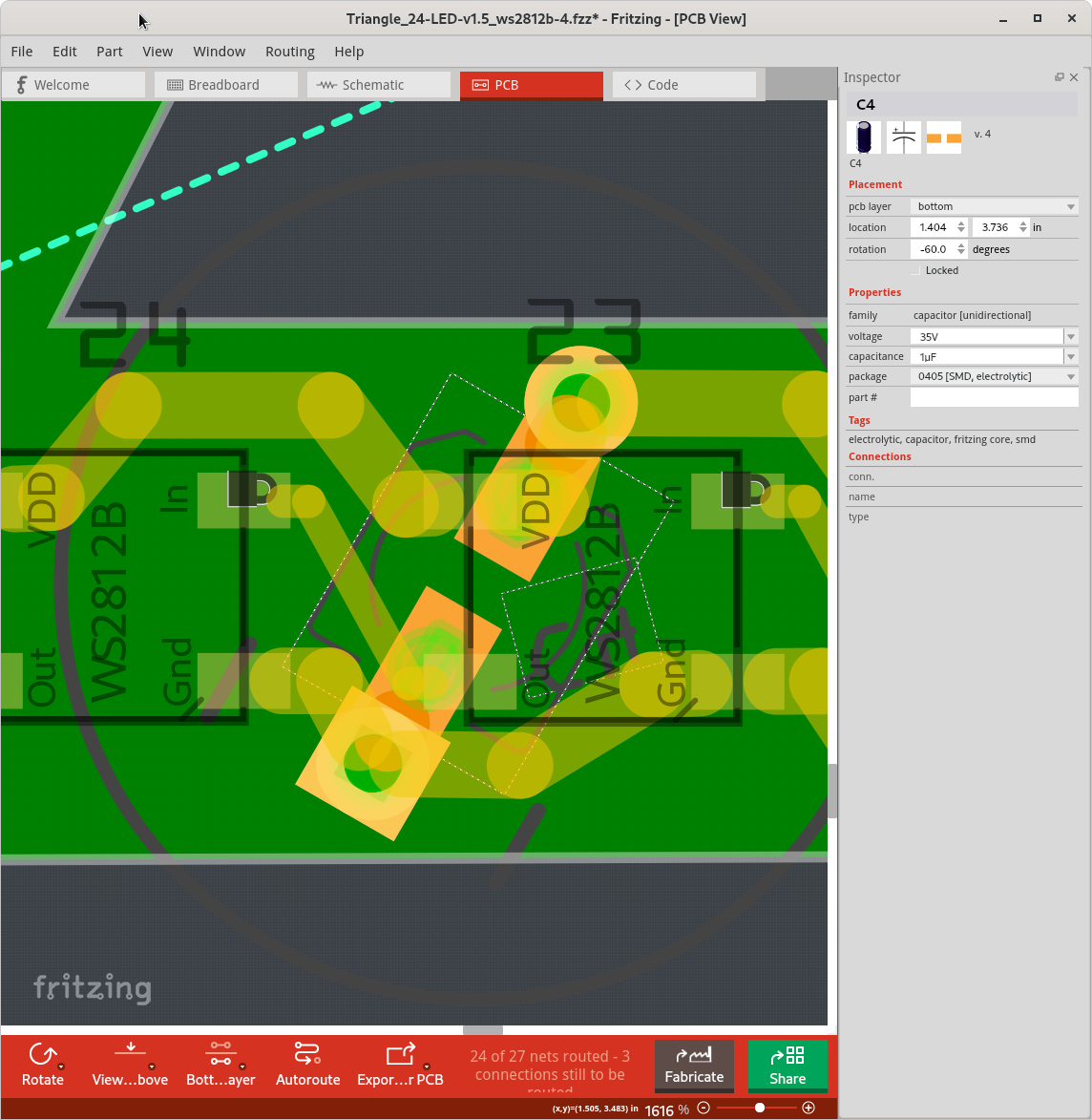
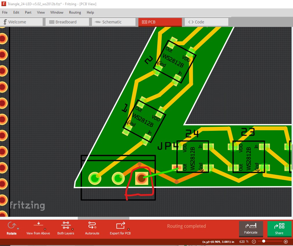
Which brings us to the serious problem. It looks like you have routing database corruption. In PCB the two pins of J4 have no rats nest lines nor connections. In schematic they are connected to VCC and ground. The best way I know of to fix this is to delete all traces in all views then reroute. To make that easier I completed schematic and completely routed it. That did not fix the problem, so I deleted all traces in schematic then re routed it completely in schematic. Then I used the rats nest lines generated from schematic in pcb to route the board manually to make sure the corruption had really cleared. That appears to be the case and as a bonus the rough route passes DRC. All these changes are contained in this sketch. I would advise checking this sketch matches what you want to do and then destroy the one that has the routing database issue (because using it probably still has the corruption which may reappear later!) I didn’t add in the bypass capacitors nor the vias for the din and dout lines but that shouldn’t be hard to do from this sketch. I would advise then making the power traces 48m instead of the current 24mils. As well JP1 seems redundant. The power is available on JP3 and JP4 as well. Again there may be a reason for it that I am not aware of.

Triangle_24-LED-v5.02_ws2812b-hoefully-not-corrupted.fzz (49.8 KB)

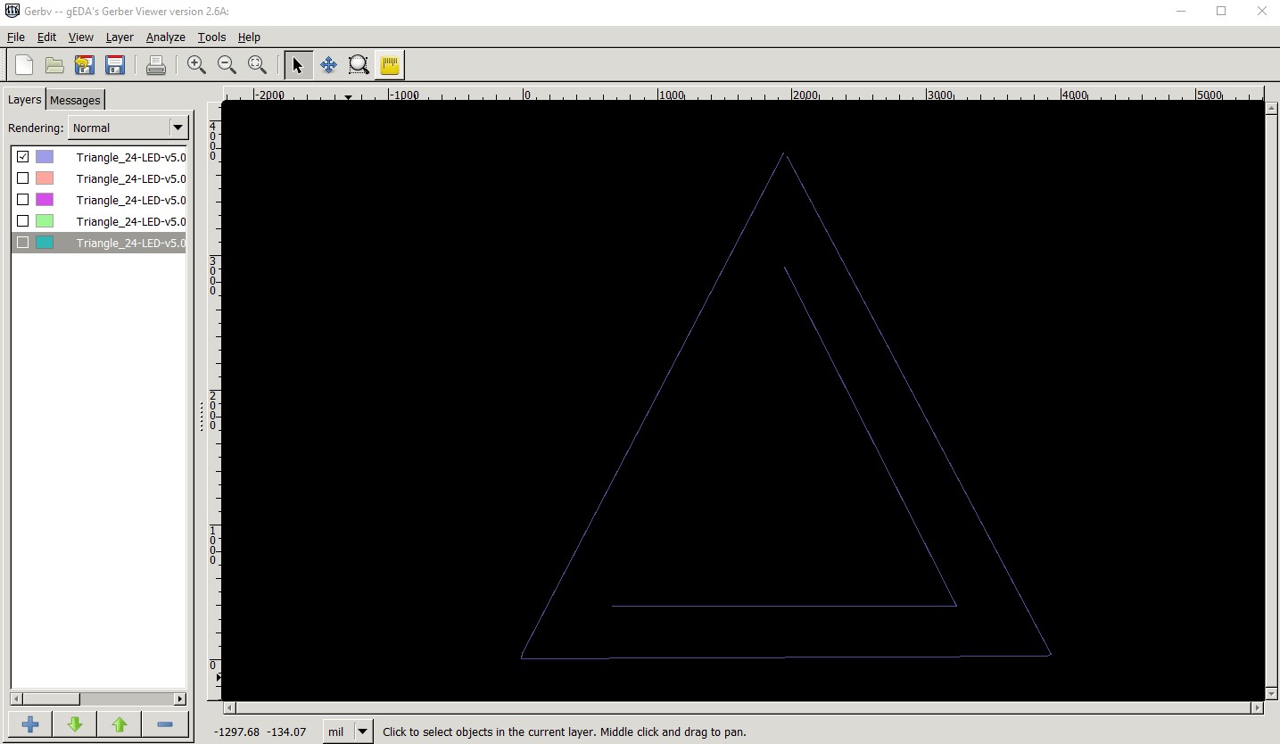
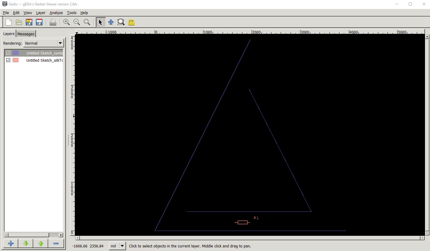
Late news: I exported pcb as geber and the gerber outline is indeed corrupted. Silkscreen looks ok (this is contour, copper0, copper1, drill and top silkscreen:

but displaying only the contour layer indicates it is corrupted and very likely won’t mill correctly.

It is missing one side of the triangle (indicating the outline svg is not correct, or there is still a Fritzing bug in path rendering (both possibilities!) Given the uneven sections in pcb view I suspect svg problems.

Peter

OK this morning i had a bash at outline editing (as usual unsuccessfully though!) I extracted your original outline svg from the .fz file then edited it in Inkscape. I removed the filters that were defined (they don’t look like they were affecting anything though.) The main problem seemed to be a mismatch between the boardoutline and silkscreen paths, that looks like what is causing the ragged edges. While I was at it I converted the triangle to being 10cm by 10cm. Unfortunately the results are even worse. I’m hoping given this svg @microMerlin can work his path magic on it (and/or correct my undoubted mistakes!) I tried adding a M command back to the start coords, after the final Z,but that doesn’t improve anything (and/or I didn’t do it right!) Here is the modified svg:

outline

and what it renders as in gerbv. The silkscreen appears to be missing completely and the path render is worse.

but has sharp corners on the bottom of the triangle :slight_smile: where it has corners.

Peter

1 Like

I wondered why the corners had those little hook like points. The dimension of the triangle were taken from the raspio Inspiring ones. They could an Isosceles triangle. Things may fit better.

The jumpers at the bottom 2 corners don’t have to be jumpers. They can be vias in order to connect 2 of the triangles together.

As for the SMD items on the board, I’m not sure I can do the soldering. I have re-flow device, but the solder paste etc and placing everything may be a bit of an undertaking.

I’ll get the board figured out first and worry about the solder later.

Do you care if the triangle is exactly 10cm by 10cm (it makes the math to create the path easier?) It looked to me (but I don’t know a lot about paths!) that the silkscreen was defined a bit differently than the boardoutline and that was somehow causing the edge distortion. The recommendation is duplicate the board outline path and change the fill and stroke which is what I did (although you see the result :slight_smile: .) We are getting a lot closer. We need to get a working outline svg and then I think we should be fine.

Peter

1 Like

10 cm x 10 cm will work.

Triangle_24-LED-v6.03_No-Jumpers.fzz (58.7 KB)

DRC is OK on this sketch.

I’m afraid we are stopped until we can produce an outline svg that Fritzing will accept. I simply don’t know enough about making paths to make the needed subtractive path to make Fritzing happy. Once we have the board shape right, then placing the LEDs and routing should be reasonably straightforward but we need a working board outline first and I at least am not good enough to make one (I have been poking at it, but as usual with no success and have given up at this point!)

Peter

1 Like