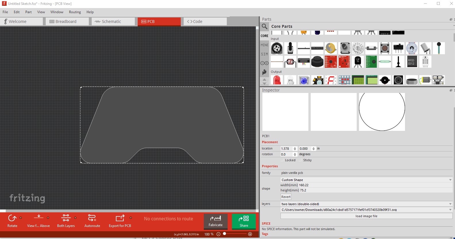
I’m brand new to making custom PCB shapes. This is my first attempt, so I’m sure I messed something up. I am using Inkscape to create the svg file and used the difference tool to create the shape. I did make slight adjustments to the edges after doing the difference operation, does that effect the way Fritzing sees cutouts? After it failed to see the cutout, I tried to recreate the whole shape by doing a difference operation on a regular rectangular box to create a stencil of the image and then doing a second difference operation to create the shape again. That did not work either.
I found a post on the forum that seemed like the issue I was having but I don’t know how to implement his solution. Making cut outs in PCB
I also found this post about absolute moves vs relative move commands in the svg file but I’m not able to fully understand what he was talking about. I do see move commands in the path property of the svg file. My custom pcb outline gerber export isn’t good help
I attached my svg. Let me know if you need anything else. Any help or advice will be greatly appreciated.
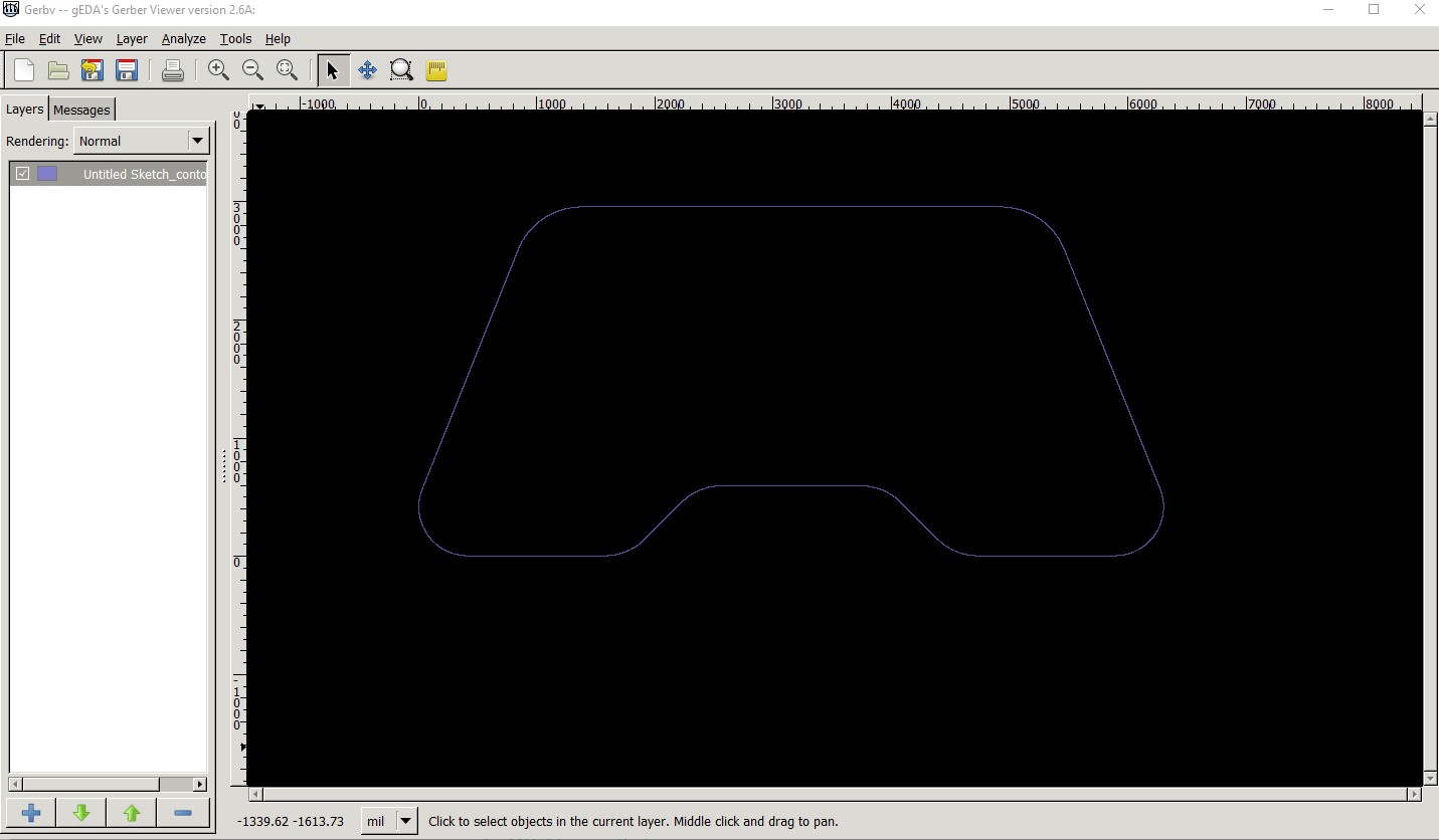
What Fritzing version are you using (some of the older ones have issues.) While your format isn’t quite correct it doesn’t seem to matter (at least for me on Fritzing 1.0.2 on Win10) it renders in Fritizng correctly (it complains about no cutouts, but you don’t have cutouts only an outline!)
Thank you Peter for taking the time to look into my issue. I have been all over these forums the last few weeks and your posts have helped me tremendously! I really admire your willingness to help others and be extremely patient with beginners. Thank you again!
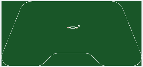
I should have said this originally but I thought I narrowed it down already. I wanted to test if my shape would work for fabrication so I uploaded the extended gerber files to JLCPCB and this is what it shows me.
I didn’t see my shape but instead it’s a rectangle and a silkscreen for my shape. It also cut the silkscreen boarder just a bit on the top and bottom of my shape. I thought this meant that my shape was not created correctly in Inkscape which led me down the rabbit hole of cutouts. Is this just how JLCPCB shows the board and it will actually be cut to the shape I want or am I requesting something from JLCPCB that they don’t do? Is JLCPCB even a good place to fabricate boards?
I have never used JLCPCB so I don’t know how it should look. All I can say is your svg produces what appears to be a correct .contour.gm1 file which should create the correct outline. You would probably have to ask JLCPCB support if your files will do the right thing for them.
I use JLCPCB for all my fab work. Many of my PCBs involve ‘shapes’ and cut-outs and I have only ever had one problem for which I accept at least partial responsibility—there are at times uncertainties in how things need to be fabricated but, with only this one exception (which involved plating through a cut-out hole, which I had placed in the Milling Layer), any such uncertainties have been resolved without my involvement.
As @vanepp suggests, contact JLCPCB Support and ask them what your board looks like when they load it up. On one occasion I also had a board where the cut-outs only appeared as an outline but I was able to confirm that the cut-outs would indeed be present on the fabricated board.