I create another part for an SHT30 (SHT3X-D1S) and not sure if I set the terminalId correctly in the Part Editor. If not, is there any documentation on how to do this?
I’ll check the part once I have time
Again part editor not very reliable. For me I use generic ICs as a base for parts.
Nope, same error.
$ FritzingCheckPartw.py part.GY-SHT30_29995a4b642655a3a2c1ebb389d9c66a_5.fzp
… (warnings deleted as irrelevant)
Warning 14: File
‘part.GY-SHT30_29995a4b642655a3a2c1ebb389d9c66a_5.fzp.bak’
At line 61
terminalId missing in schematicView (likely an error)
In theory (although it rarely works for me) you can do it in parts editor like this:

select pin 1 (which is really connector0 in the .fzp file which you are changing to confuse matters) and click on the “w” (for west) icon to select the orientation of the terminalId and that should do it. As noted for me it rarely does. This is probably covered in Old_Grey’s video tutorials (as he unlike me was able to make it work, although I could not even with his explanations!) The way I make parts (and FritzingCheckPart.py) is covered in my tutorial.
Fritzing PART CREATION Video Tutorial Series
I lately learned there aren’t links to the videos in Old_Grey’s tutorial so you need to do a google search for the title and then they come up on YouTube.
Peter
Hi Peter also discovered some prblems
@dapostol73 Couple of problems here
The part
GY-SHT3-_HumidityTemperatureSensor-fixed.fzpz (5.1 KB)
First unzip your .fzpz file to get
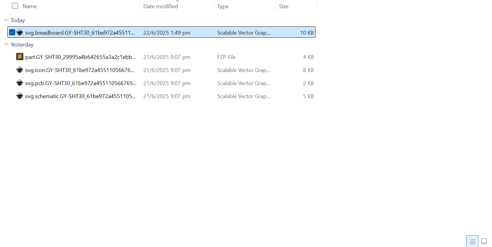
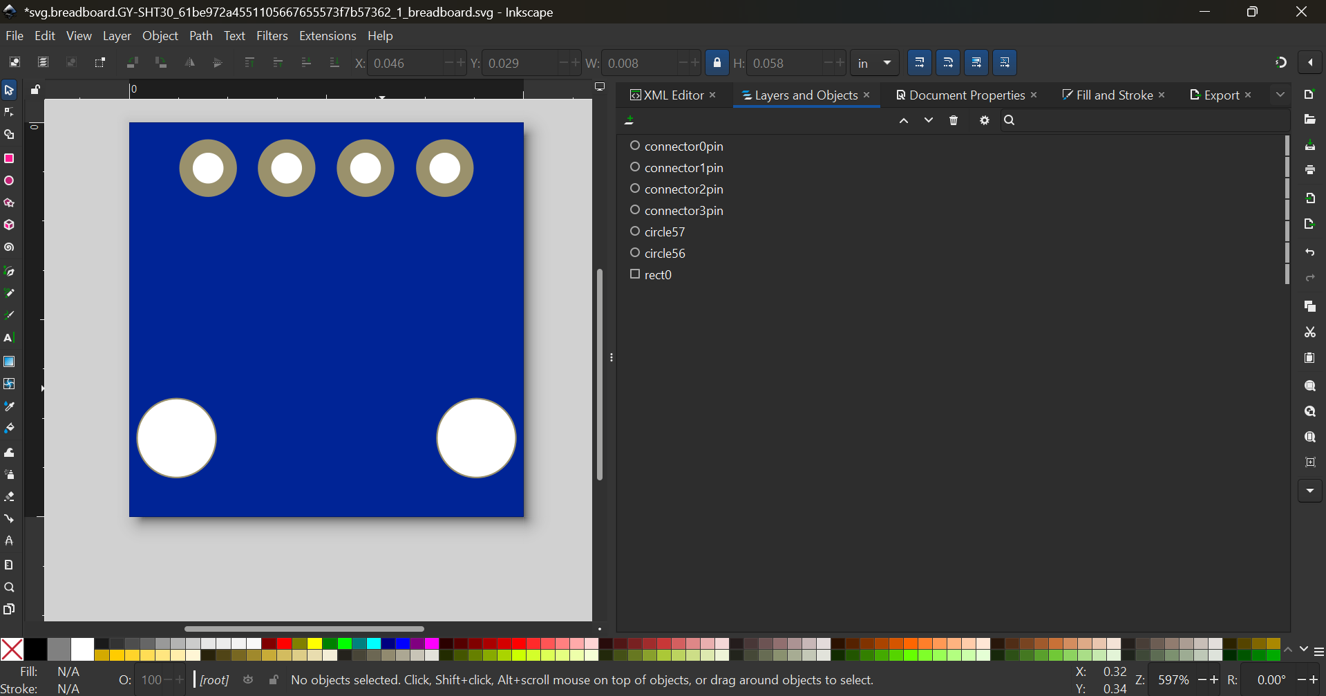
Breadboard
First, there’s a stray element here

To solve that issue, delete it
Next, the connectors are slightly off by 0.001in. To fix set the SCL connector to 0.163
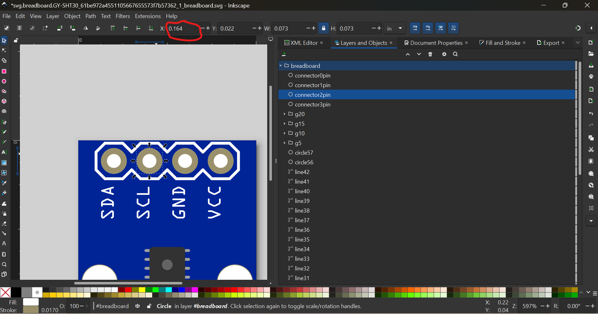
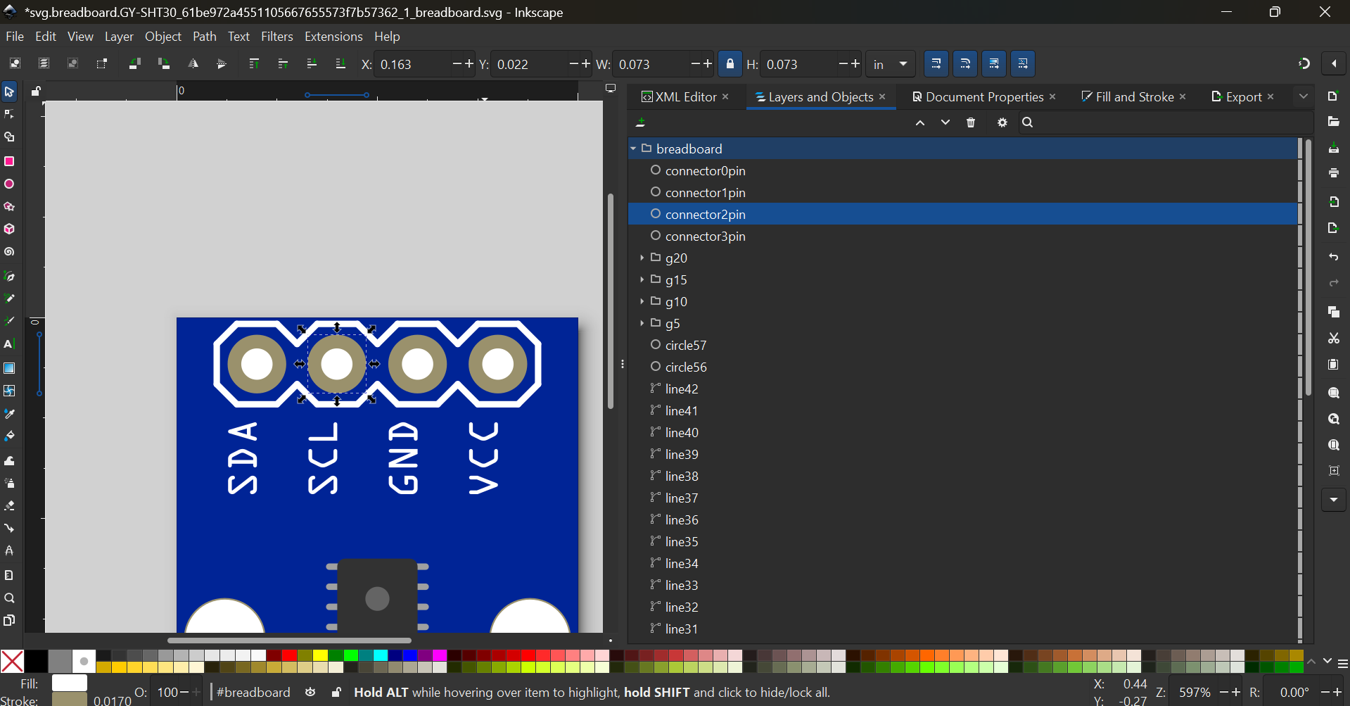
Do the same for the GND connector.
Schematic
The terminalIDs are a little suspicious
See that crooket wire
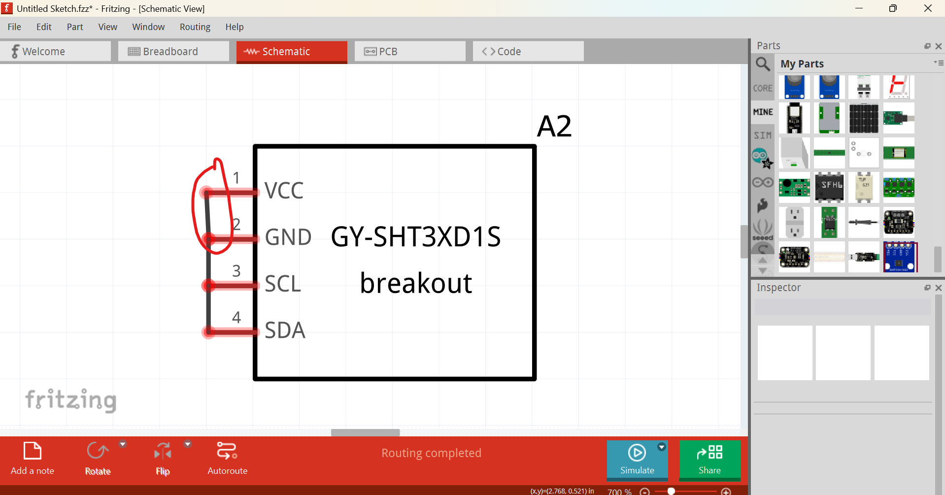
To fix, delete the entire schematic and redo with Randy’s Inkscape Schematic Extension
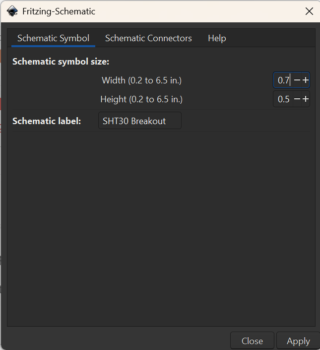
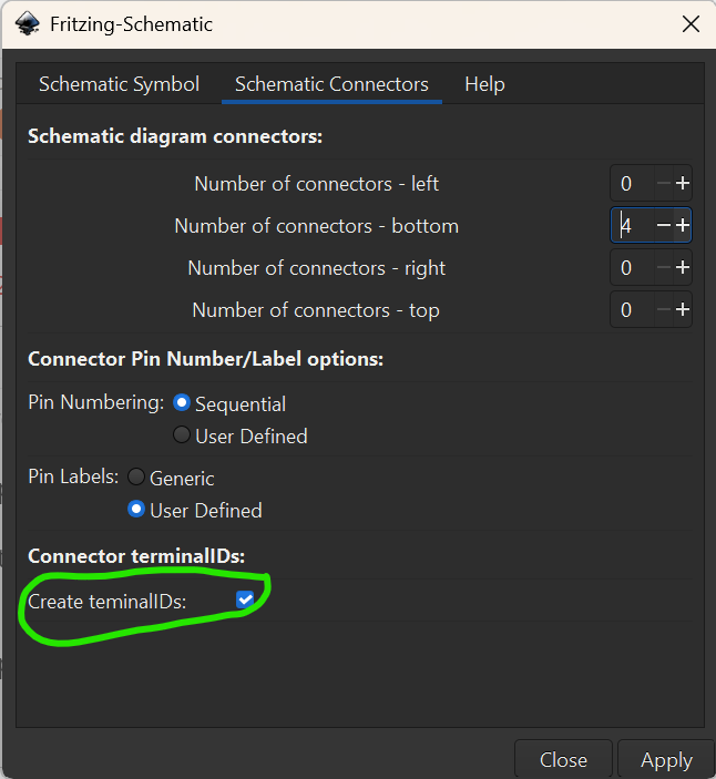
Set the connectors
- VCC
- GND
- SCL
- SDA
Click apply and you’ll get this
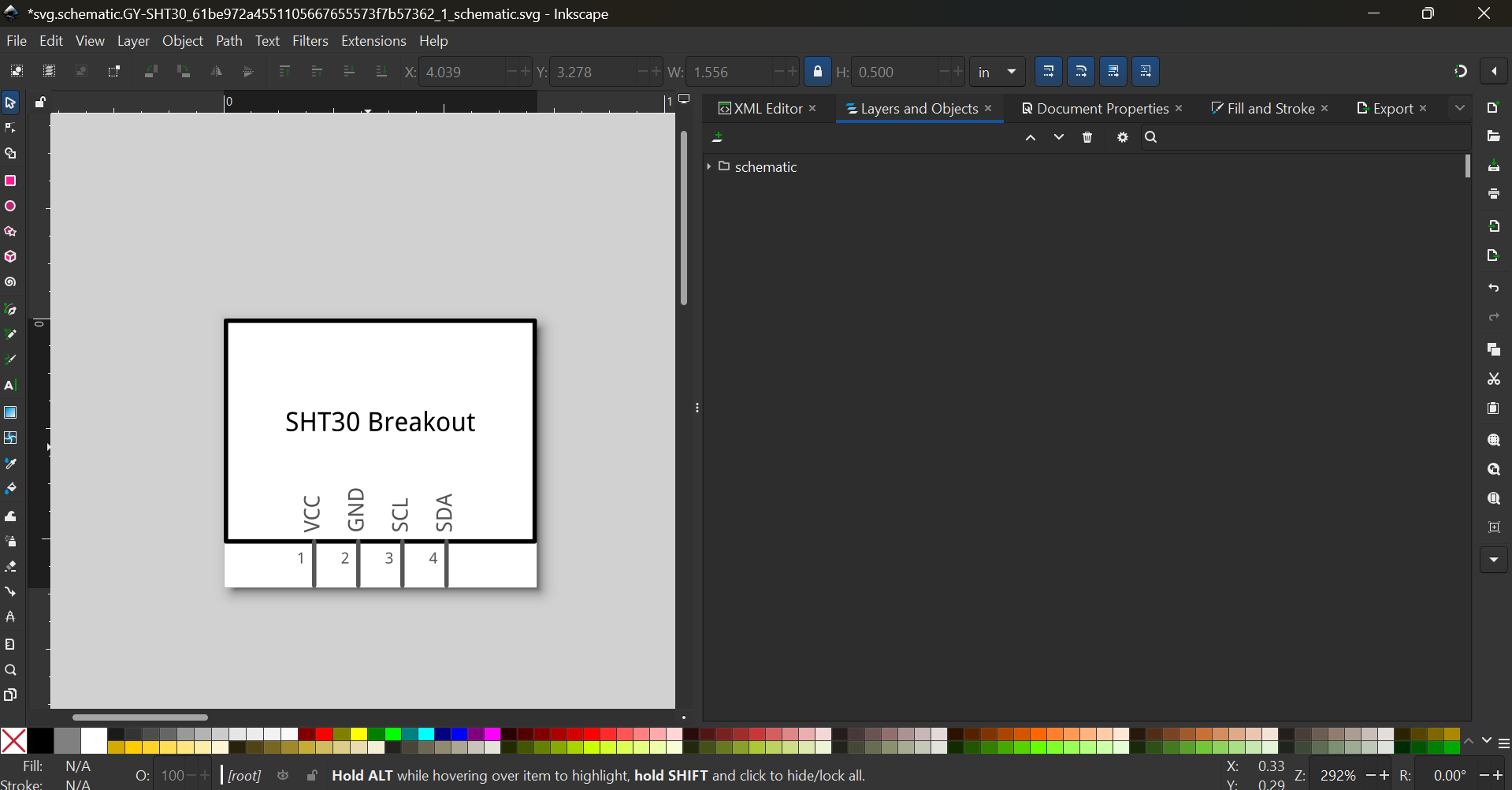
Save the file and done
PCB
Another bout of more severe problems
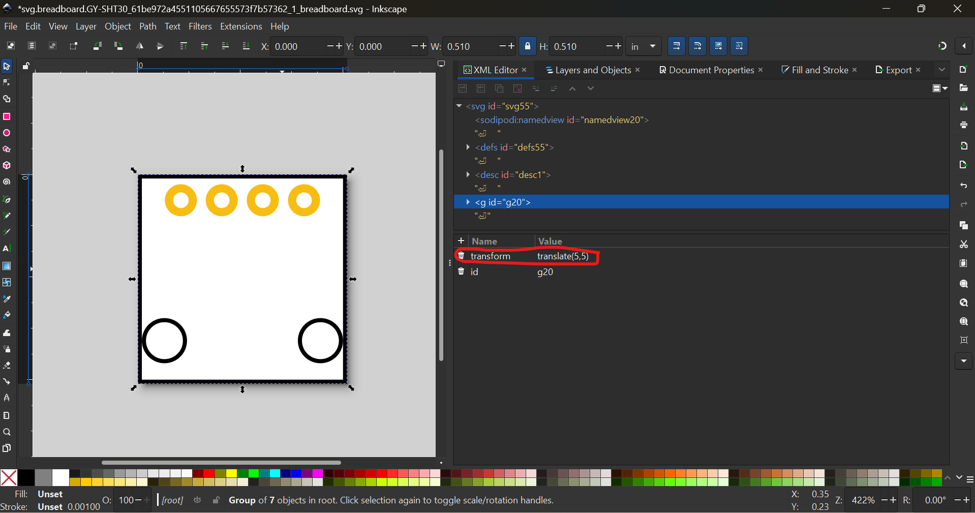
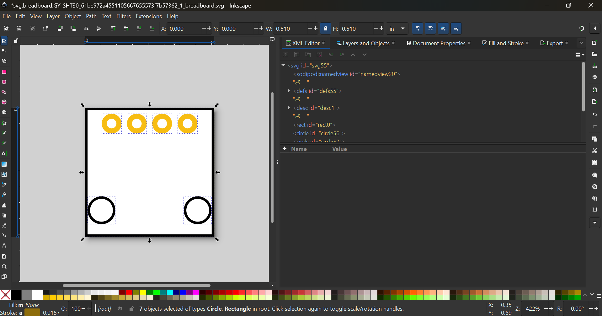
First start with breadboard and Ctrl+Shift+G or Cmd+Shift+G to ungroup everything
Next, delete everything except the connectors, board and the holes
Next go to XML editor and (with connector0pin selected) change from

to
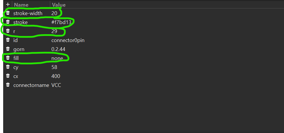
Do the same for the others
Next go to the hole and change from
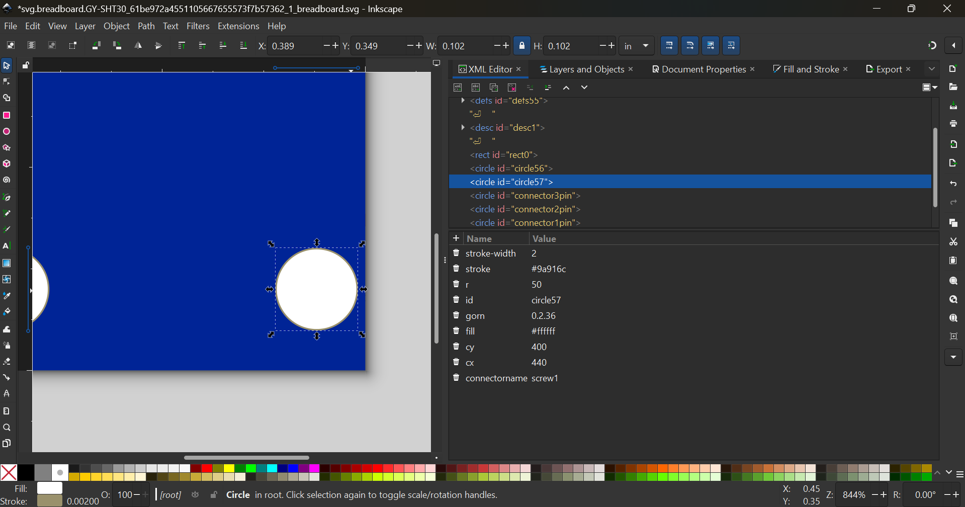
to

Do the same for the other screw.
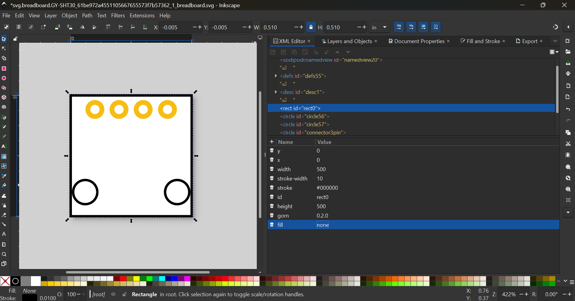
For the rectangle, change from

to
Now go to edit → select all → ctrl/cmd+G to group
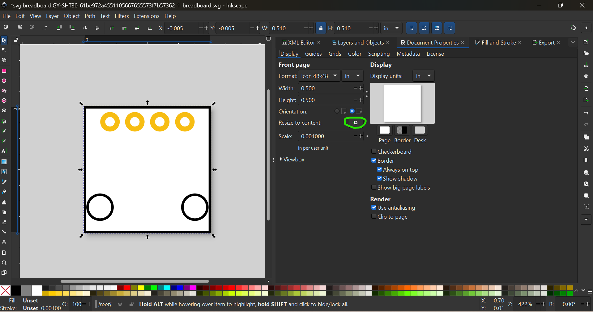
Reset the viewbox
then ungroup to remve the transforms
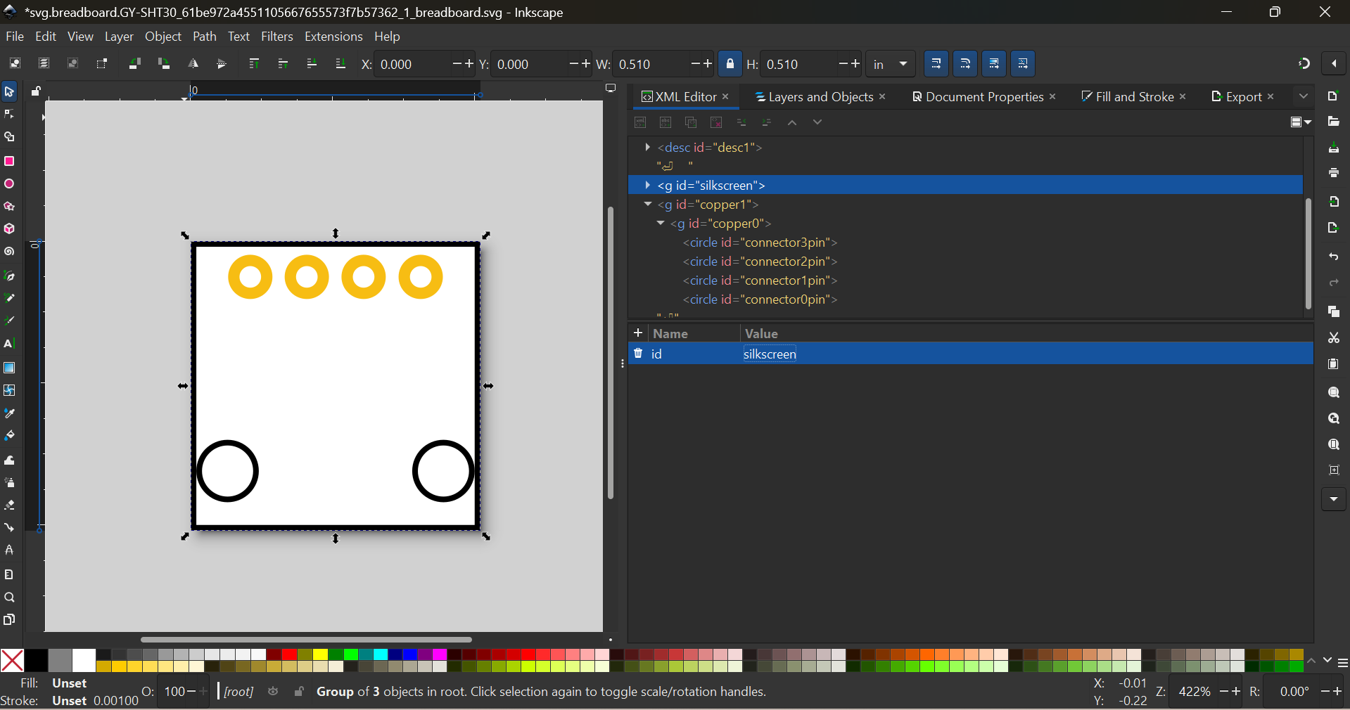
Group the connectors twice

and rename to

Group the rest
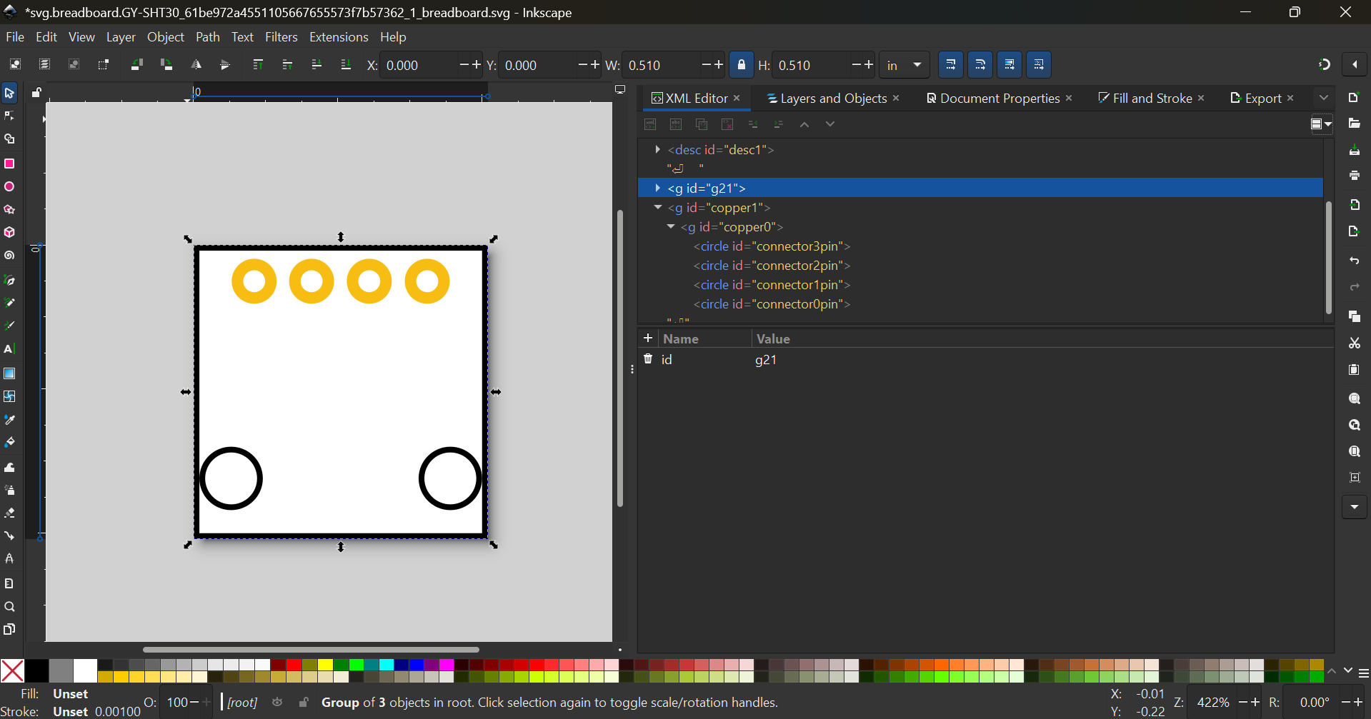
and rename to
On to .fzp file
.fzp file
Some changes – please change from
<tags>
 <tag>GY-SGP30  Breakout</tag>
 <tag>contrib</tag>
 <tag>fritzing user</tag>
</tags>
to
<tags>
 <tag>GY-SHT30  Breakout</tag>
 <tag>contrib</tag>
 <tag>fritzing user</tag>
</tags>
Remove the description (change from
<description><!DOCTYPE HTML PUBLIC "-//W3C//DTD HTML 4.0//EN" "http://www.w3.org/TR/REC-html40/strict.dtd">
<html><head><meta name="qrichtext" content="1" /><meta charset="utf-8" /><style type="text/css">
p, li { white-space: pre-wrap; }
hr { height: 1px; border-width: 0; }
li.unchecked::marker { content: "\2610"; }
li.checked::marker { content: "\2612"; }
</style></head><body style=" font-family:'Segoe UI'; font-size:9pt; font-weight:400; font-style:normal;">
<p style=" margin-top:0px; margin-bottom:0px; margin-left:0px; margin-right:0px; -qt-block-indent:0; text-indent:0px;">GY-SHT30 Breakout</p></body></html></description>
to
<description></description>
Now for the views change from
 <views>
  <iconView>
   <layers image="icon/GY-SHT30_61be972a4551105667655573f7b57362_1_icon.svg">
    <layer layerId="icon"/>
   </layers>
  </iconView>
  <breadboardView>
   <layers image="breadboard/GY-SHT30_61be972a4551105667655573f7b57362_1_breadboard.svg">
    <layer layerId="breadboard"/>
   </layers>
  </breadboardView>
  <schematicView>
   <layers image="schematic/GY-SHT30_61be972a4551105667655573f7b57362_1_schematic.svg">
    <layer layerId="schematic"/>
   </layers>
  </schematicView>
  <pcbView>
   <layers image="pcb/GY-SHT30_61be972a4551105667655573f7b57362_1_pcb.svg">
    <layer layerId="silkscreen"/>
    <layer layerId="copper1"/>
    <layer layerId="copper0"/>
   </layers>
  </pcbView>
 </views>
to
<views>
  <iconView>
   <layers image="breadboard/GY-SHT30_61be972a4551105667655573f7b57362_1_breadboard.svg">
    <layer layerId="icon"/>
   </layers>
  </iconView>
  <breadboardView>
   <layers image="breadboard/GY-SHT30_61be972a4551105667655573f7b57362_1_breadboard.svg">
    <layer layerId="breadboard"/>
   </layers>
  </breadboardView>
  <schematicView>
   <layers image="schematic/GY-SHT30_61be972a4551105667655573f7b57362_1_schematic.svg">
    <layer layerId="schematic"/>
   </layers>
  </schematicView>
  <pcbView>
   <layers image="pcb/GY-SHT30_61be972a4551105667655573f7b57362_1_pcb.svg">
    <layer layerId="silkscreen"/>
    <layer layerId="copper1"/>
    <layer layerId="copper0"/>
   </layers>
  </pcbView>
 </views>
Next in the .fzp fike there are missing connectorIDs, which why I say the part editor won’t change. To fix, change from
<connector id="connector0" name="Pin 1" type="male">
   <description>VCC</description>
   <views>
    <breadboardView>
     <p layer="breadboard" svgId="connector0pin"/>
    </breadboardView>
    <schematicView>
     <p layer="schematic" svgId="connector0pin"/>
    </schematicView>
    <pcbView>
     <p layer="copper1" svgId="connector0pin"/>
     <p layer="copper0" svgId="connector0pin"/>
    </pcbView>
   </views>
  </connector>
to
 <connectors>
  <connector id="connector0" name="Pin 1" type="male">
   <description>VCC</description>
   <views>
    <breadboardView>
     <p layer="breadboard" svgId="connector0pin"/>
    </breadboardView>
    <schematicView>
     <p layer="schematic" svgId="connector0pin" terminalID="connector0terminal"/>
    </schematicView>
    <pcbView>
     <p layer="copper1" svgId="connector0pin"/>
     <p layer="copper0" svgId="connector0pin"/>
    </pcbView>
   </views>
  </connector>
After which save the file, zip the folder into a .fzpz file.
Thanks for the @RAPTOR7762 still learning. Currently I’ve been hand editing the SVG, what editor are you using to create/modify them? And good to know the fzpz is just a zip file.
Inkscape is open source (and thus free) and gives the best control of the svg is what I use. Illustrator works, but older versions will only dimension svgs in px which causes scaling issues. you can import them to parts editor and it will convert them, but it is extra work.
Peter