Name of the part
North America Residential Load Center
GenericNA32CircuitLoadCenter.fzpz (75.2 KB)
Current_Transformer_PZCT02_Smaller_Side_View.fzpz (5.4 KB)
Top view
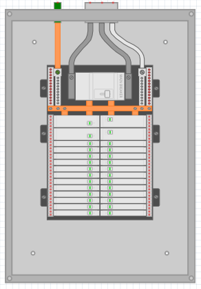
Example
ESPHome Power Monitor
Name of the part
North America Residential Load Center
GenericNA32CircuitLoadCenter.fzpz (75.2 KB)
Current_Transformer_PZCT02_Smaller_Side_View.fzpz (5.4 KB)
Top view
Example
ESPHome Power Monitor
Your part has a number of problems. FritzingCheckPart.py has this to say about it (edited for length):
…
Warning 19: File
‘svg.breadboard.NAGenericUtilityPanel001_f4e5e973aa4b719c30a1aa0d470b17e1_43_breadboard.svg.bak’
At line 2
Height 400px is defined in px
in or mm is a better option (px can cause scaling problems!)
…
Error 69: File
‘svg.breadboard.NAGenericUtilityPanel001_f4e5e973aa4b719c30a1aa0d470b17e1_43_breadboard.svg.bak’
At line 17
Found a drawing element before a layerId (or no layerId)
Warning 14: File
‘part.NAGenericUtilityPanel001_7566471799b70f70a61f5a80b7c1c3ee_34.fzp.bak’
At line 1324
terminalId missing in schematicView (likely an error)
…
Error 69: File
‘svg.breadboard.NAGenericUtilityPanel001_f4e5e973aa4b719c30a1aa0d470b17e1_43_breadboard.svg.bak’
At line 17
Found a drawing element before a layerId (or no layerId)
Error 18: File
‘part.NAGenericUtilityPanel001_7566471799b70f70a61f5a80b7c1c3ee_34.fzp.bak’
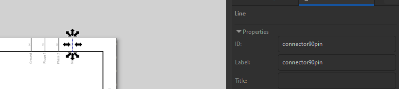
Connector connector90pin is in the fzp file but not the svg file. (typo?)
svg svg.pcb.NAGenericUtilityPanel001_f4e5e973aa4b719c30a1aa0d470b17e1_43_pcb.svg.bak
Error 18: File
‘part.NAGenericUtilityPanel001_7566471799b70f70a61f5a80b7c1c3ee_34.fzp.bak’
Connector connector91pin is in the fzp file but not the svg file. (typo?)
svg svg.pcb.NAGenericUtilityPanel001_f4e5e973aa4b719c30a1aa0d470b17e1_43_pcb.svg.bak
Error 18: File
‘part.NAGenericUtilityPanel001_7566471799b70f70a61f5a80b7c1c3ee_34.fzp.bak’
Connector connector92pin is in the fzp file but not the svg file. (typo?)
svg svg.pcb.NAGenericUtilityPanel001_f4e5e973aa4b719c30a1aa0d470b17e1_43_pcb.svg.bak
Error 18: File
‘part.NAGenericUtilityPanel001_7566471799b70f70a61f5a80b7c1c3ee_34.fzp.bak’
Connector connector93pin is in the fzp file but not the svg file. (typo?)
svg svg.pcb.NAGenericUtilityPanel001_f4e5e973aa4b719c30a1aa0d470b17e1_43_pcb.svg.bak
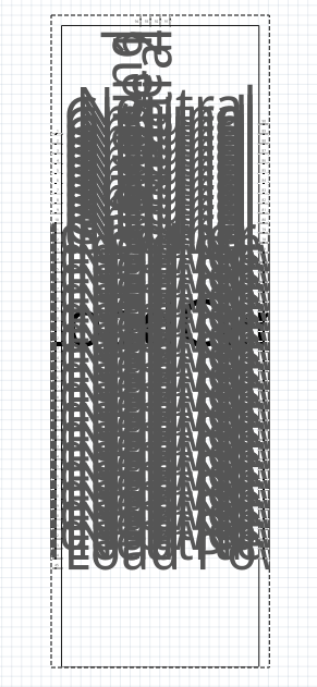
The missing terminatIds are being added by Fritzng (but that doesn’t always work and only in late version Fritizng earlier versions will connect in the center of the pin.) The lack of a breadboard layerId means that the part won’t export as an image (it will be a blank in the image.) Possibly due to the px as dimensions, schematic doesn’t align to the grid as it should. It is possible that Fritzing has guessed wrong about what the scale value should be or the svg just may not be aligned properly. Also your font sizes are much too small (note the size of the text circled in red in this image.)
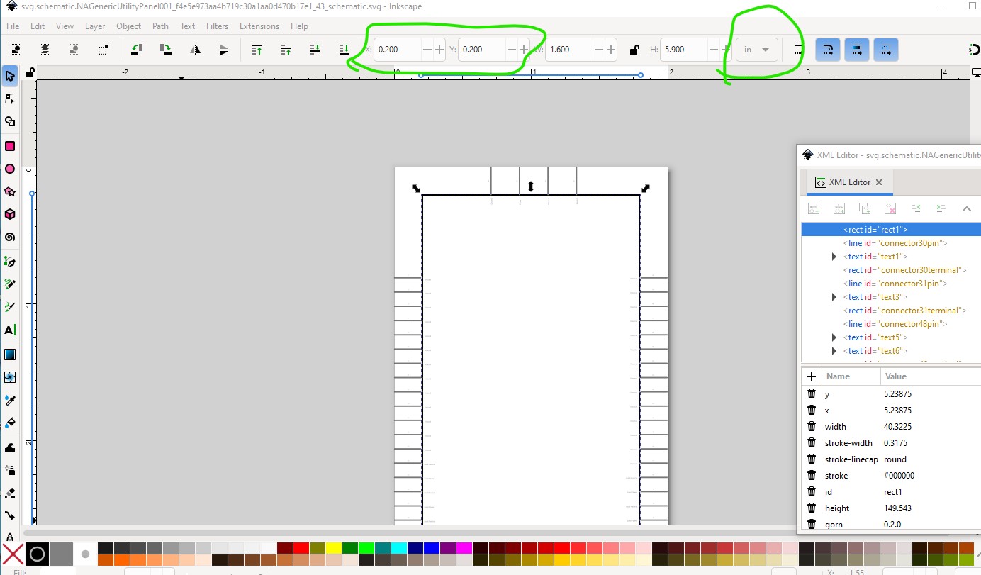
The svg is dimensioned correctly in inches, so the pins are misaligned (which requires either manual changing or assuming you are using Inkscape as your svg editor using Randy’s schematic extension to replace schematic completely!) Here I did it manually. As an aside the text circled in red needs to move in to the schematic group, where it is it won’t export as an image.
Fixing that is a little difficult since the scale of the svg isn’t the Fritzing standard (which FritzingCheckPart complained about but I ignored as it doesn’t cause any errors.) First lets look at the pin alignment. The rectangle is correct aligned on 0.1in boundaries.
but the pins are incorrect as they are not on 01.in boundaries
As noted I would use Randy’s Inkscape extension to make a new schematic, but you can manually adjust all the pins although it is a lot of work with so many pins. So on to correcting the font size. Here is a correctly scaled schematic with the first pin replaced with your text (to make it the same size in both svgs)
the font size is set to 49px as specified in the part file format document, but because of the scale change the height and width measurements of the text are what is of interest here. This is the current (too small value of the font size. To correct it I increased the font size by trial and error to get the dimensions close to what the correct svg is.
that produces this correctly sized text (and the font size can then be copied to the other text via xml editor in Inkscape!)
I also changed the fill to the correct #555555 color. Pcb is currently broken due to some pins (circled in red here) not being defined in the svg file. That causes the red circle where those pins are placed in the middle of the part.
Your best bet would be to suppress pcb view. Instructions on how to do that can be found in this tutorial (although it requires editing the fzp file to achieve, parts editor can’t make this change AFAIK.)
Hope this helps, if you have questions feel free to ask. Always happy to help people make good parts.
Peter
Thanks for those tips, I’m not sure about some of them
These connectors seem to all be here why does it say it’s missing?
Or that is for the PCB view?
The font sizes were not that small until I exported it but I accepted that as the other error I had were they were way to big and sideways.
I’m not sure about that g60 node as it is not showing in my xml editor but maybe it got changed when I ran it through the partchecker.
I’m not sure where the 400 px settings are set I set them to mm in the page and still got the error
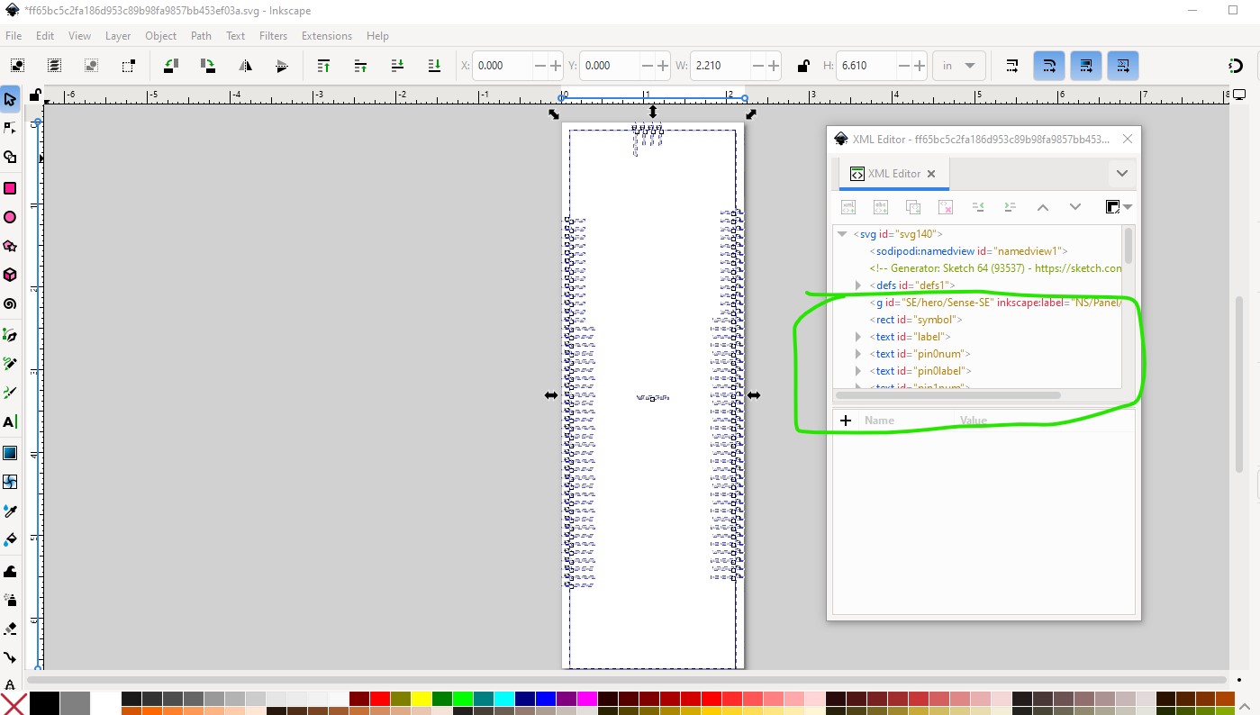
Here is the generated schematic

When I use extension it looks fine in inkscape but then when I import the graphic the text has the opposite effect, very large text.
Also the pins on one side don’t match the pins on the other side seems to put them up one pin higher.
The page you pointed to about PCB design doesn’t seem to have the directions about removal of the PCB stuff (suppress?) or I just don’t know what I am looking for.
by 01.in boundaries do you mean the pins should be on the lines of the grid?
C:\Users\nonasuomy\Downloads\FritzingCheckPart-master\FritzingCheckPart-master>python FritzingCheckPart.py C:\Users\nonasuomy\Documents\Fritzing\parts\user\NAGenericUtilityPanel001_7566471799b70f70a61f5a80b7c1c3ee_34.fzp
File
'C:\Users\nonasuomy\Documents\Fritzing\parts\user\NAGenericUtilityPanel001_7566471799b70f70a61f5a80b7c1c3ee_34.fzp.bak'

This is a smd part as only the copper1 view is present.
If you wanted a through hole part add the copper0 definition before line 46

Modified 4: File
'C:\Users\nonasuomy\Documents\Fritzing\parts\user\..\svg\user\breadboard/NAGenericUtilityPanel001_f4e5e973aa4b719c30a1aa0d470b17e1_43_breadboard.svg.bak'
At line 4

ReferenceFile

'UtilityPanel.svg'

doesn't match input file

'NAGenericUtilityPanel001_f4e5e973aa4b719c30a1aa0d470b17e1_43_breadboard.svg'

Corrected

Modified 4: File
'C:\Users\nonasuomy\Documents\Fritzing\parts\user\..\svg\user\schematic/NAGenericUtilityPanel001_f4e5e973aa4b719c30a1aa0d470b17e1_43_schematic.svg.bak'
At line 8

ReferenceFile

'mega2560_schematic.svg'

doesn't match input file

'NAGenericUtilityPanel001_f4e5e973aa4b719c30a1aa0d470b17e1_43_schematic.svg'

Corrected

Modified 4: File
'C:\Users\nonasuomy\Documents\Fritzing\parts\user\..\svg\user\pcb/NAGenericUtilityPanel001_f4e5e973aa4b719c30a1aa0d470b17e1_43_pcb.svg.bak'
At line 5

ReferenceFile

'sparkfun-digitalic_tqfp100_pcb.svg'

doesn't match input file

'NAGenericUtilityPanel001_f4e5e973aa4b719c30a1aa0d470b17e1_43_pcb.svg'

Corrected

Modified 3: File
'C:\Users\nonasuomy\Documents\Fritzing\parts\user\..\svg\user\pcb/NAGenericUtilityPanel001_f4e5e973aa4b719c30a1aa0d470b17e1_43_pcb.svg.bak'
At line 111

Silkscreen stroke color #f0f0f0 isn't white or black. Set to black.

Modified 3: File
'C:\Users\nonasuomy\Documents\Fritzing\parts\user\..\svg\user\pcb/NAGenericUtilityPanel001_f4e5e973aa4b719c30a1aa0d470b17e1_43_pcb.svg.bak'
At line 112

Silkscreen stroke color #f0f0f0 isn't white or black. Set to black.

Modified 3: File
'C:\Users\nonasuomy\Documents\Fritzing\parts\user\..\svg\user\pcb/NAGenericUtilityPanel001_f4e5e973aa4b719c30a1aa0d470b17e1_43_pcb.svg.bak'
At line 113

Silkscreen stroke color #f0f0f0 isn't white or black. Set to black.

Modified 3: File
'C:\Users\nonasuomy\Documents\Fritzing\parts\user\..\svg\user\pcb/NAGenericUtilityPanel001_f4e5e973aa4b719c30a1aa0d470b17e1_43_pcb.svg.bak'
At line 114

Silkscreen stroke color #f0f0f0 isn't white or black. Set to black.

Modified 3: File
'C:\Users\nonasuomy\Documents\Fritzing\parts\user\..\svg\user\pcb/NAGenericUtilityPanel001_f4e5e973aa4b719c30a1aa0d470b17e1_43_pcb.svg.bak'
At line 115

Silkscreen stroke color #f0f0f0 isn't white or black. Set to black.

Modified 3: File
'C:\Users\nonasuomy\Documents\Fritzing\parts\user\..\svg\user\pcb/NAGenericUtilityPanel001_f4e5e973aa4b719c30a1aa0d470b17e1_43_pcb.svg.bak'
At line 116

Silkscreen stroke color #f0f0f0 isn't white or black. Set to black.

Modified 3: File
'C:\Users\nonasuomy\Documents\Fritzing\parts\user\..\svg\user\pcb/NAGenericUtilityPanel001_f4e5e973aa4b719c30a1aa0d470b17e1_43_pcb.svg.bak'
At line 117

Silkscreen stroke color #f0f0f0 isn't white or black. Set to black.

Modified 3: File
'C:\Users\nonasuomy\Documents\Fritzing\parts\user\..\svg\user\pcb/NAGenericUtilityPanel001_f4e5e973aa4b719c30a1aa0d470b17e1_43_pcb.svg.bak'
At line 118

Silkscreen stroke color #f0f0f0 isn't white or black. Set to black.

Modified 3: File
'C:\Users\nonasuomy\Documents\Fritzing\parts\user\..\svg\user\pcb/NAGenericUtilityPanel001_f4e5e973aa4b719c30a1aa0d470b17e1_43_pcb.svg.bak'
At line 119

Silkscreen stroke color #f0f0f0 isn't white or black. Set to black.

Warning 6: File
'C:\Users\nonasuomy\Documents\Fritzing\parts\user\NAGenericUtilityPanel001_7566471799b70f70a61f5a80b7c1c3ee_34.fzp.bak'
At line 2

ReferenceFile name

'sparkfun-digitalic-atmega2560-au.fzp'

Doesn't match fzp filename

'NAGenericUtilityPanel001_7566471799b70f70a61f5a80b7c1c3ee_34.fzp'

Warning 14: File
'C:\Users\nonasuomy\Documents\Fritzing\parts\user\NAGenericUtilityPanel001_7566471799b70f70a61f5a80b7c1c3ee_34.fzp.bak'
At line 1324

terminalId missing in schematicView (likely an error)

Warning 14: File
'C:\Users\nonasuomy\Documents\Fritzing\parts\user\NAGenericUtilityPanel001_7566471799b70f70a61f5a80b7c1c3ee_34.fzp.bak'
At line 1338

terminalId missing in schematicView (likely an error)

Warning 14: File
'C:\Users\nonasuomy\Documents\Fritzing\parts\user\NAGenericUtilityPanel001_7566471799b70f70a61f5a80b7c1c3ee_34.fzp.bak'
At line 1352

terminalId missing in schematicView (likely an error)

Warning 14: File
'C:\Users\nonasuomy\Documents\Fritzing\parts\user\NAGenericUtilityPanel001_7566471799b70f70a61f5a80b7c1c3ee_34.fzp.bak'
At line 1366

terminalId missing in schematicView (likely an error)

Warning 19: File
'C:\Users\nonasuomy\Documents\Fritzing\parts\user\..\svg\user\breadboard/NAGenericUtilityPanel001_f4e5e973aa4b719c30a1aa0d470b17e1_43_breadboard.svg.bak'
At line 2

Height 400px is defined in px
in or mm is a better option (px can cause scaling problems!)

Warning 19: File
'C:\Users\nonasuomy\Documents\Fritzing\parts\user\..\svg\user\breadboard/NAGenericUtilityPanel001_f4e5e973aa4b719c30a1aa0d470b17e1_43_breadboard.svg.bak'
At line 2

Width 270px is defined in px
in or mm is a better option (px can cause scaling problems!)

Warning 23: File
'C:\Users\nonasuomy\Documents\Fritzing\parts\user\..\svg\user\breadboard/NAGenericUtilityPanel001_f4e5e973aa4b719c30a1aa0d470b17e1_43_breadboard.svg.bak'
At line 2591

Key -inkscape-font-specification
value Droid Sans is invalid and has been deleted

Warning 25: File
'C:\Users\nonasuomy\Documents\Fritzing\parts\user\..\svg\user\pcb/NAGenericUtilityPanel001_f4e5e973aa4b719c30a1aa0d470b17e1_43_pcb.svg.bak'
At line 110

Silkscreen layer should be above the copper layers for easier selection
in pcb view


Error 69: File
'C:\Users\nonasuomy\Documents\Fritzing\parts\user\..\svg\user\breadboard/NAGenericUtilityPanel001_f4e5e973aa4b719c30a1aa0d470b17e1_43_breadboard.svg.bak'
At line 10

Found a drawing element before a layerId (or no layerId)

Error 69: File
'C:\Users\nonasuomy\Documents\Fritzing\parts\user\..\svg\user\schematic/NAGenericUtilityPanel001_f4e5e973aa4b719c30a1aa0d470b17e1_43_schematic.svg.bak'
At line 5

Found a drawing element before a layerId (or no layerId)

Error 18: File
'C:\Users\nonasuomy\Documents\Fritzing\parts\user\NAGenericUtilityPanel001_7566471799b70f70a61f5a80b7c1c3ee_34.fzp.bak'

Connector connector90pin is in the fzp file but not the svg file. (typo?)

svg C:\Users\nonasuomy\Documents\Fritzing\parts\user\..\svg\user\pcb/NAGenericUtilityPanel001_f4e5e973aa4b719c30a1aa0d470b17e1_43_pcb.svg.bak

Error 18: File
'C:\Users\nonasuomy\Documents\Fritzing\parts\user\NAGenericUtilityPanel001_7566471799b70f70a61f5a80b7c1c3ee_34.fzp.bak'

Connector connector91pin is in the fzp file but not the svg file. (typo?)

svg C:\Users\nonasuomy\Documents\Fritzing\parts\user\..\svg\user\pcb/NAGenericUtilityPanel001_f4e5e973aa4b719c30a1aa0d470b17e1_43_pcb.svg.bak

Error 18: File
'C:\Users\nonasuomy\Documents\Fritzing\parts\user\NAGenericUtilityPanel001_7566471799b70f70a61f5a80b7c1c3ee_34.fzp.bak'

Connector connector92pin is in the fzp file but not the svg file. (typo?)

svg C:\Users\nonasuomy\Documents\Fritzing\parts\user\..\svg\user\pcb/NAGenericUtilityPanel001_f4e5e973aa4b719c30a1aa0d470b17e1_43_pcb.svg.bak

Error 18: File
'C:\Users\nonasuomy\Documents\Fritzing\parts\user\NAGenericUtilityPanel001_7566471799b70f70a61f5a80b7c1c3ee_34.fzp.bak'

Connector connector93pin is in the fzp file but not the svg file. (typo?)

svg C:\Users\nonasuomy\Documents\Fritzing\parts\user\..\svg\user\pcb/NAGenericUtilityPanel001_f4e5e973aa4b719c30a1aa0d470b17e1_43_pcb.svg.bak
This one is a Fritzing quirk. The problem is that you have px in the font-size. To fix this you can either run the part through FritzingCheckPart.py (which will automatically fix this) or probably easier in the short term, edit all you svgs with a text editor and do a global remove of the px in the file like this:
  <g id="schematic">
    <rect fill="none" height="6500.0" width="2000.0" stroke-width="10" stroke="#000000" stroke-linejoin="round" stroke-linecap="round" id="symbol" x="105" y="105"/>
    <text x="1105" y="3355" font-family="'Droid Sans'" font-size="60px" fill="#000000" id="label" text-anchor="middle">NALoadCenter</text>
    <text x="75" y="1185" text-anchor="end" font-family="Droid Sans" font-size="35" fill="#555555" id="pin0num">1</text>
    <text x="125" y="1217" text-anchor="start" font-family="'Droid Sans'" font-size="49px" fill="#555555" id="pin0label">Ground</text>
This "font-size=“60px” is a problem and most svg editors add the px for CSS compliance which causes the fault in Fritzing (I’m hoping to get a fix for this, there is a discussion on this in another thread here:
Edit Breadboard Icon Failed - #16 by vanepp
with one of the developers, so I have some hope he may find a fix. Until then either FritzingCheckPart.py or a global replace of “px” with “” in a text editor should fix this (there may be cases where it won’t but I have not yet run in to one!) Suppressing pcb view again requires a text editor, you need to edit the .fzp file (in your case this one)
part.NAGenericUtilityPanel001_7566471799b70f70a61f5a80b7c1c3ee_34.fzp
and replace this
    <pcbView>
      <layers image="pcb/NAGenericUtilityPanel001_f4e5e973aa4b719c30a1aa0d470b17e1_43_pcb.svg">
        <layer layerId="copper1"/>
        <layer layerId="silkscreen"/>
      </layers>
    </pcbView>
with this from here (earlier in the file)
    <breadboardView>
      <layers image="breadboard/NAGenericUtilityPanel001_f4e5e973aa4b719c30a1aa0d470b17e1_43_breadboard.svg">
        <layer layerId="breadboard"/>
      </layers>
    </breadboardView>
but with only part of it which will reuse the breadboard view as pcb, As far as I know parts editor can’t do this only editing the fzp file directly, but it has the effect of making pcb view a blank (as Fritzing requires something to render in pcb view, but knows that breadboard is the wrong layerId and thus doesn’t render it but is happy it has something render!)
      <layers image="breadboard/NAGenericUtilityPanel001_f4e5e973aa4b719c30a1aa0d470b17e1_43_breadboard.svg">
        <layer layerId="breadboard"/>
to give this:
    <pcbView>
      <layers image="breadboard/NAGenericUtilityPanel001_f4e5e973aa4b719c30a1aa0d470b17e1_43_breadboard.svg">
        <layer layerId="breadboard"/>
      </layers>
    </pcbView>
Those two should fix all your issues I think. The px problem works the same in breadboard, so it needs to be done there too.
Yes, because by default snap to grid is enabled and the wires will snap to the 0.1in grid (which is the default) so in breadboard and schematic your parts need to align to the grid (i.e. the elements need to be 0.1in apart) to align correctly with other parts. You will notice the generated schematic aligns on exactly 0.1in boundaries. It looks like you have a copy of FritzingCheckPart.py, so if you use the svgs it wrote (the originals are in the .bak files) they should work correctly if the pin alignment is correct (FritzingCheckPart won’t adjust the pin spacing.) It should remove all the px from the font-size and stop the large text. The pin offset in schematic is an extension quirk, it can be fixed in two ways: reduce the size of the height of the svg in the extension so it is shorter (so the pins are on the same level) or what is probably easier, is edit the svg from this
first ungroup the svg so you can easily move things (at least in Inkscape!)
then use the tool bar to move the left side up in 0.1in increments to the new position.
Do the same to the right side.
then reduce the height of the rectangle to make the schematic smaller (which is desirable!)
then do an Edit->select all and Edit->resize page to selection to reset the viewbox and an Object->group to re make the layerId group and name it schematic then save the svg as plain svg (I imagine your svg editor will have similar commands, hopefully one that moves by 0.1in increments or this gets very painful!) Hope this helps, if not feel free to ask!
Peter
Most text editors should have this. Peter uses Cygwin, and I use Sublime text — both have global replace