Changing the layout of the buttons is not really top priority , Infact , I think it’ll look cooler being asymmetric , and other than that , everything looks great according to the screenshot ! (My laptops gone for repair rn ![]()
![]()
![]() so I can’t view the file ) , but thank you so much for helping me out here , now the only thing left is the routing part I guess , we don’t need anything else do we ?
so I can’t view the file ) , but thank you so much for helping me out here , now the only thing left is the routing part I guess , we don’t need anything else do we ?
Nope, if you are good with it as it stands I’ll route it.
Peter
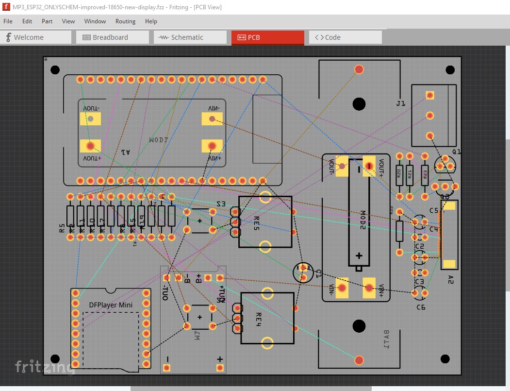
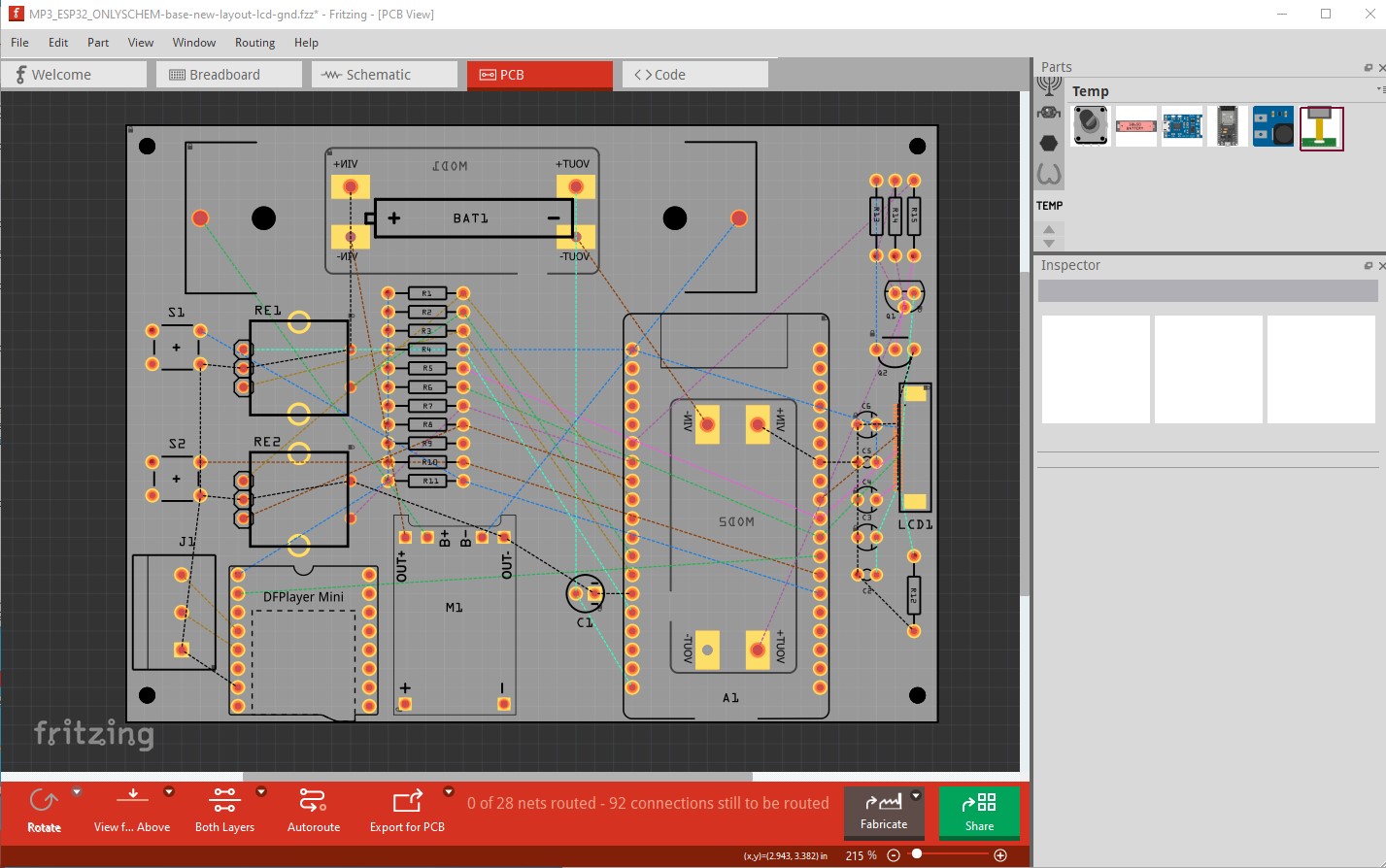
As usual routing the board indicates there are better ways to lay things out. Some of them (swapping the order of resistors to simplify routing) I have already done, but there are a tow major ones: making sure all the USB connectors are on one edge of the case, and not running the audio wires all the way across the board are worth making changes for. The board (mostly routed already) looks like this
before routing
now
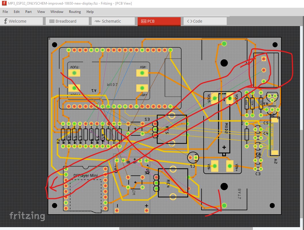
the audio connection really needs to move next to the MP3 player to reduce the lead length on the audio, that is likely the most important. Then rotating the ESP so its USB connector is also coming out the bottom (and possibly clearing the antenna more) are also worth doing I think. The encoders, and switches will remain pretty much where they are. I’m going to try this and see if it works out. If it doesn’t I will continue routing the current layout.
Peter
Ahh sure sure , the audio connection can be moved no problem , whatever you think is right please do it , I just woke up and I replied to you asap
I’m currently routing an improved version with the changes, it looks like ir should route (I was concerned there wasn’t enough space for traces, but it looks to be OK. It will probably take in to tomorrow to finish it though.
edit
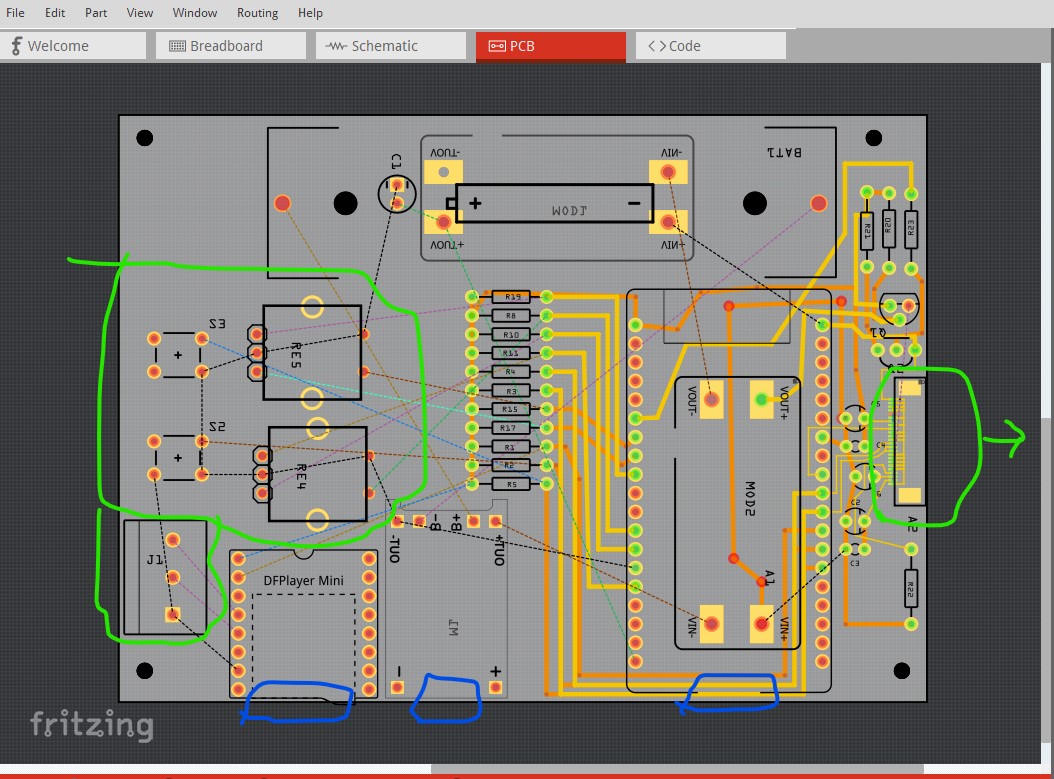
The layout is far enough along so I can display it so you can object if you don’t like it. It looks like I have managed to cause database corruption somehow (because I have a rats nest line without a connection) so there is a good chance I will have to start again. The switches and encoder are more or less in the center of the board and towards the left side so as to avoid other components. The audio screw terminals are right beside the MP3 player not running all the way across the board which is I think the most important change. The display will I think take the cable out in the direction of the arrow to allow you to mount it on the case (it looks to have a good length of cable.) It would be really wise to breadboard this as I don’t know if the display connections are correct. Given the fpc cable that may not be easy but a variety of people sell adapter boards that split a fpc out to 0.1 headers to mount on a breadboard. All the three slots (1 CF card for the MP3 and two usb connectors) come out on the bottom rather than one on another edge. That should make mechanical assembly a lot easier and is the other major reason for doing this.
Peter
Damnnn this looks really neat man ,all the ports are lined up on one side , however it looks like routing it is gonna be extremely hard looking at all the overlapping ![]()
![]()
It would require some planning — laying out bottom layer traces and top layer traces ![]()
It was a little exciting around the display connector, but other than apparently running in to the routing database bug again (but this time I know approximately what I was doing, so may be able to recreate it which will get it fixed, which would be good for all of us!) it looks like it should work fine. It needs some clean up but the hard parts are already done successfully. I should have it later today.
Peter
Yooo lesgoo , what was causing the routing error ?
Ahh I see I see, seriously though watching you two give your opinions and work shows me how much I have to learn , I’m seriously grateful for y’all ![]()
I think (but will have to try and reproduce it to be sure) that it was caused by me trying to jumper the pins of the display together to create the ground daisy chain. If that is correct (and I am lucky!) that should recreate it which will allow it to be fixed. The first instance of this error took me 5 years of trying before I reproduced it and the developers found and fixed a bunch of bugs that had been present for more than 10 years so I’m not surprised there still appear to be more bugs.
Peter
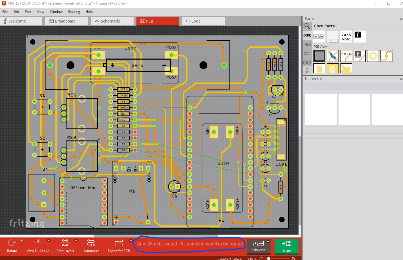
getting close only 5 more connections to route but enough for tonight. I’ll continue tomorrow.
Peter
Oh that is interesting! Let’s hope it doesn’t take 5 years again ![]()
![]()
![]()
Holy shi this looks soo neat and clean , and I did not know that you could route a connection using both the top layer and bottom layer , that is really interesting!
You just have to right-click the trace and set to the layer you want.
Ahhh I see , I understand now
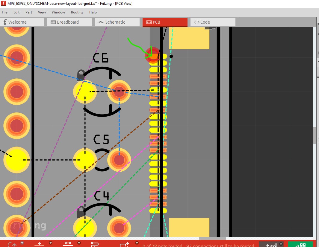
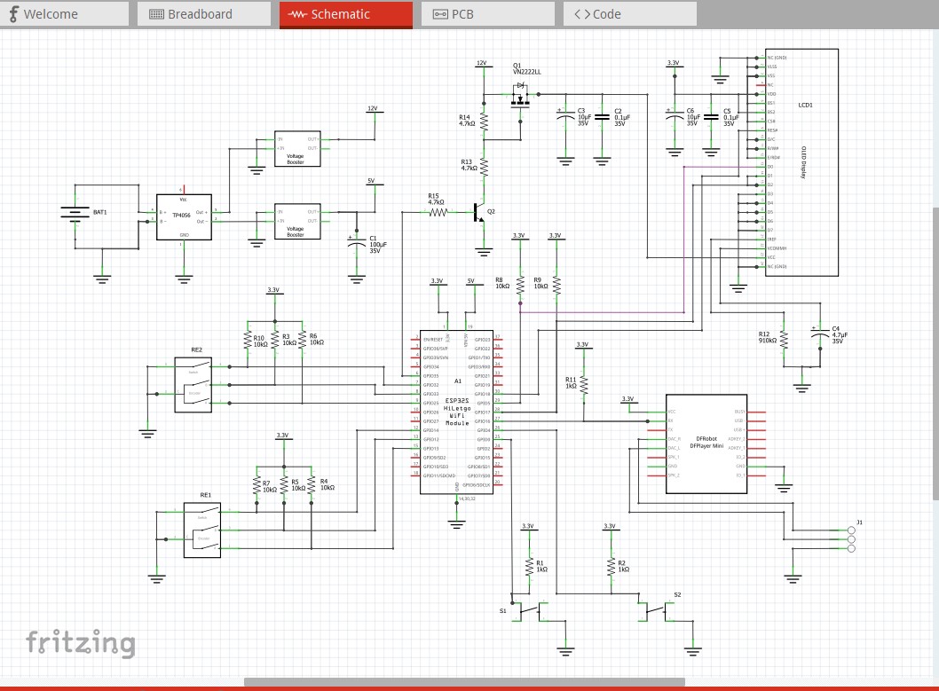
OK finally done I think. I tried ground fill, but it hits a bug (or I did something wrong I don’t often do ground fill!) So we can’t use that. Here is an look at how I routed this (it isn’t entirely complete because I managed to lose a couple of images last night!) In the middle of routing I discovered I screwed up in schematic and reversed power and ground on the 12V boost supply, luckily it was labeled in pcb view and I saw ground going to the positive pin and checked schematic and it was indeed wrong. You need to prototype this (at least parts of it) before ordering boards. They make adapters that will convert a fpc socket to 0.1in dip a google search like “24 pin fpc prototyping adapters .5mm pitch” will find them from various people with various prices. I think it is essential that you verify the display circuitry works correctly before ordering boards especially the power supply sequencing and probably the display itself too. OK on to how I did this, I started from this with schematic complete (if wrong at this point!)
Then I set the grid size to 0.5mm in pcb and started routing the fpc connector, starting with all the ground connections (which is fairly messy due to Fritzing quirks.) Right clicking on pin1 (the green arrow in the image) lights all the ground pins yellow. I am only concerned with the fpc connector for the moment so started there.
Connect pin1 to pin2 then change the resulting wire from 24mils to 8mils (super fine) then drag it out from the pin. It should extend the wire keeping both connections but it doesn’t It disconnects the connection and extends a wire from one pin. So create a bend point in the wire and drag its end back to pin2 where it should go to make the connection. This process is where I think I caused the routing corruption but this time things worked correctly so it looks like it won’t be easy to reproduce. I’ll continue poking at it in a bit before reporting it as a bug.
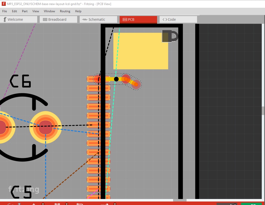
That produces a direct shortest path route to pin 1 like this. While this will work it isn’t desirable so create a bend point by clicking on the wire
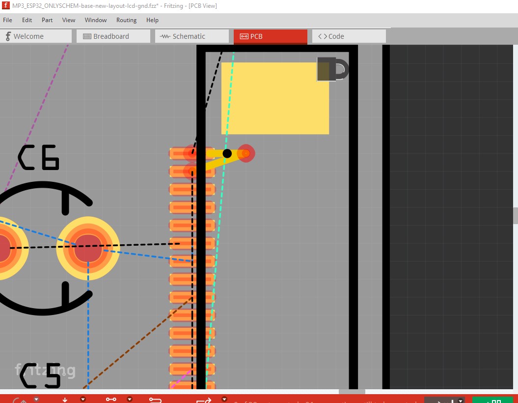
and make it look like this

The ground connections completed
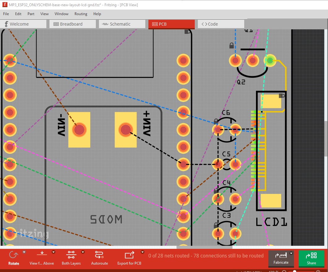
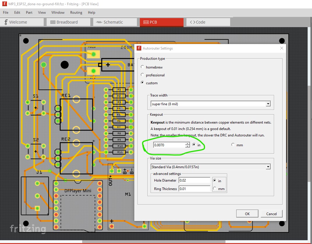
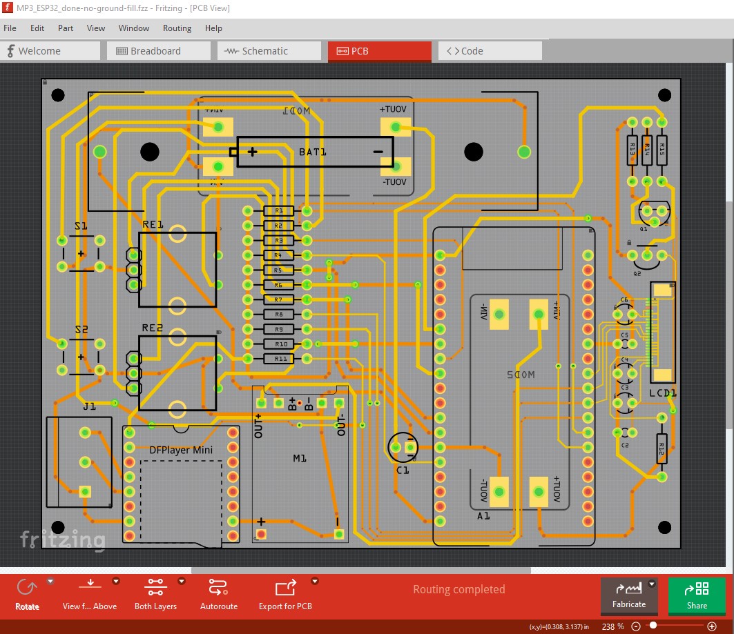
Now continue on and route the rest of the board. Note best practice in pcb design is to route traces horizontal, vertical or at 45 degrees so I automatically do that. Completing the routing produces this sketch which is fully routed (if not tested!) and passes DRC with the clearance set to 0.07in to allow for the 0.5mm pitch of the fpc connector. Routing->Autorouter/DRC settings to set it and change the default 0.01in to 0.007in like this
That produces this sketch
MP3_ESP32_done-no-ground-fill.fzz (205.0 KB)
which looks like this
I also tried ground fill which would have been desirable if it worked, but there appears to be a bug (which I will report!) so this isn’t usable as it shorts 3.3V
MP3_ESP32_DO_NOT_USE-ground-fill.fzz (305.9 KB)
It produces this (which is desirable)
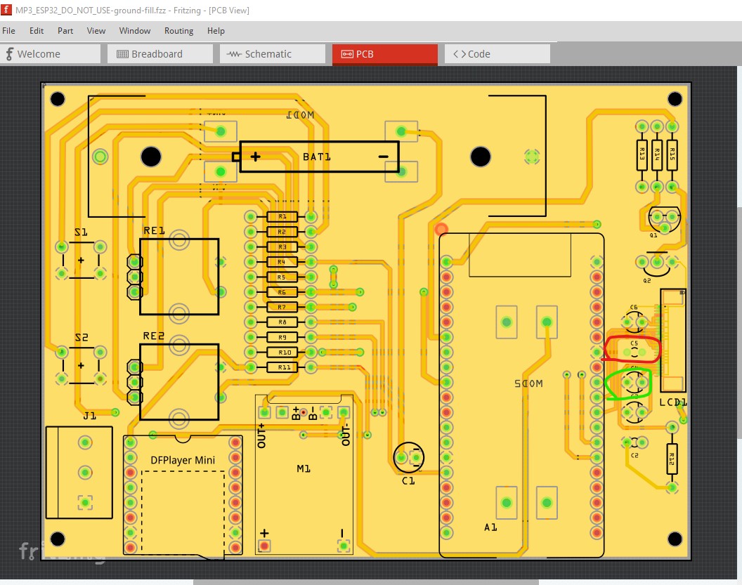
except for the capacitor which is circled in red and shorts 3.3V. Although interestingly DRC reports no error. It is especially obvious in the gerber output (which is where I found it!) A closer view of the problem in Fritzing
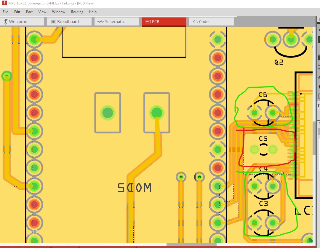
although I missed it (because I didn’t expect it) when I looked at it. But in the gerber output it is much more obvious.
the coppertop layer displayed in gerbv
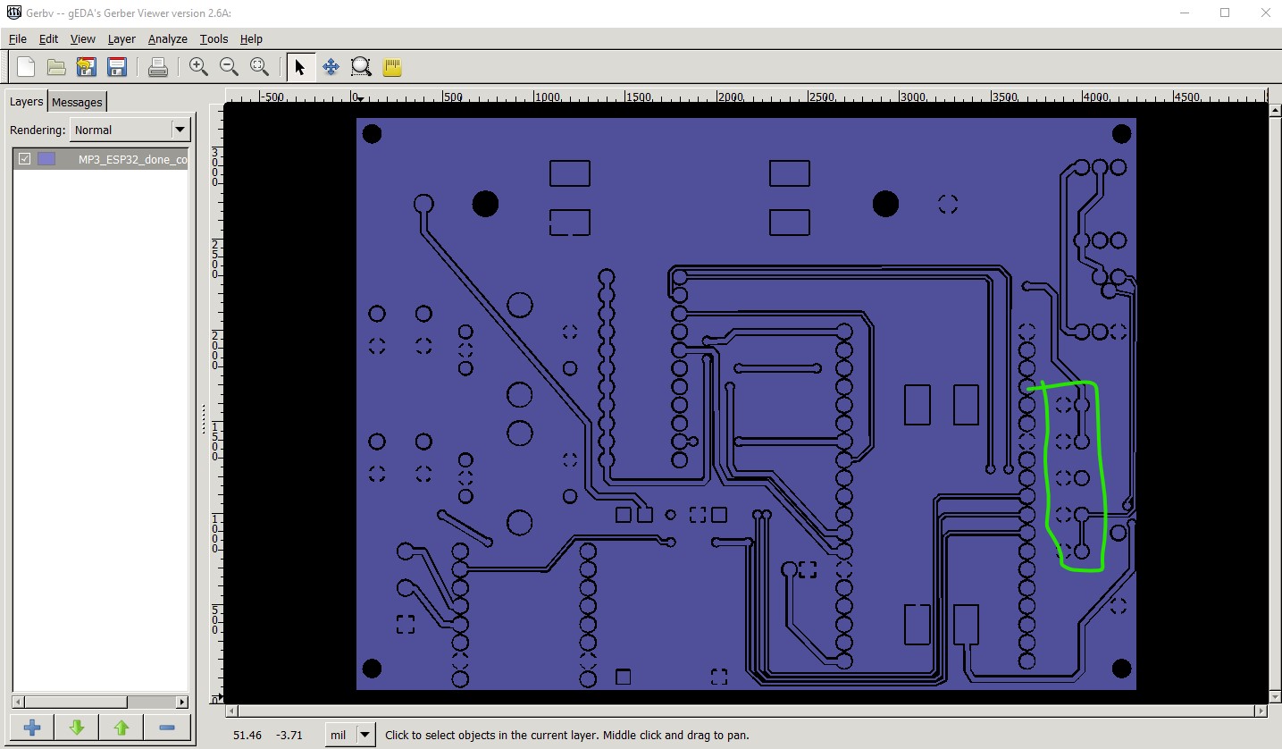
and a zoomed in view of the same area. The copper is shorting the capacitor and thus shorts 3.3V to ground which is fatal.

Peter
That ground fill bug sounds nasty—super lucky you caught it in the Gerber stage. I’ll definitely skip using ground fill for now and double-check power vs ground connections in both schematic and PCB view.
I’ll also prototype the display part first like you suggested—especially the 12V sequencing and OLED behaviour. I’ll look into getting one of those 0.5mm pitch FPC-to-DIP adapters to test properly on breadboard.
Thanks again for the routing tips and DRC clearance settings! This helped a lot ![]()
Will keep you posted as I test it out!
The only way to get good at routing boards is to practice (I have been doing it for more that 50 years now) so feel free to take the sketch and in pcb Routing-> select all traces and hit delete to delete them and then then do Routing->select all vias and again press delete to delete them. Now see if you can replicate pcb for your self (and if you have problems feel free to post!)
Peter
Thanks so much for the advice and the encouragement! Really appreciate you sharing your experience — 50 years is incredible. I’ll definitely give it a shot by redoing the routing myself from scratch. Great idea to delete all traces and vias and try it independently — it’ll be a solid learning experience. If I hit a wall, I’ll be sure to ask for help. Thanks again! ![]()