Feel free to post the part and we will comment on improvements / shortcomings. In Fritzing right click on the part in the mine parts bin and then click export to get an fzpz file and post that.
By and large looks fine, a couple of minor points. In the pcb svg copper0 should be under copper1 (doing an indent node on the copper0 group will fix that) the result is you only have a copper0 (bottom) pad in the gerbers, the top pad is missing… Your hole sizes are a little non standard. the terminal holes show as being 0.511 (1.3 mm) in the pdf but are 0.066743 in the gerbers, my list of free drill sizes from a local pcb supplier indicates .0520 or .0595 as free drill sizes so you may want to switch to one of those (and.or check with your favorite fab house for their list). For the mounting hole, .125 shows as a free size so you may want to switch to that (although the current 0.106 matches their hole, larger by a bit shouldn’t hurt).
Not a problem, although I rarely make boards so you would be best to post the completed board here for some of the more experienced folks to look over and run the design rules checker under routing.
A gerber viewer (use gerbv from the geda project, but there are online ones and other packages) to look at the gerbers that the board will be made from is also a good bet. Good luck!
Don’t know that one . I’d expect their web page should have a standard drill size chart, otherwise I think (remembering I don’t do boards much ) most fabs round odd drill sizes up to the next size they support. With luck someone with more experience making boards will reply.
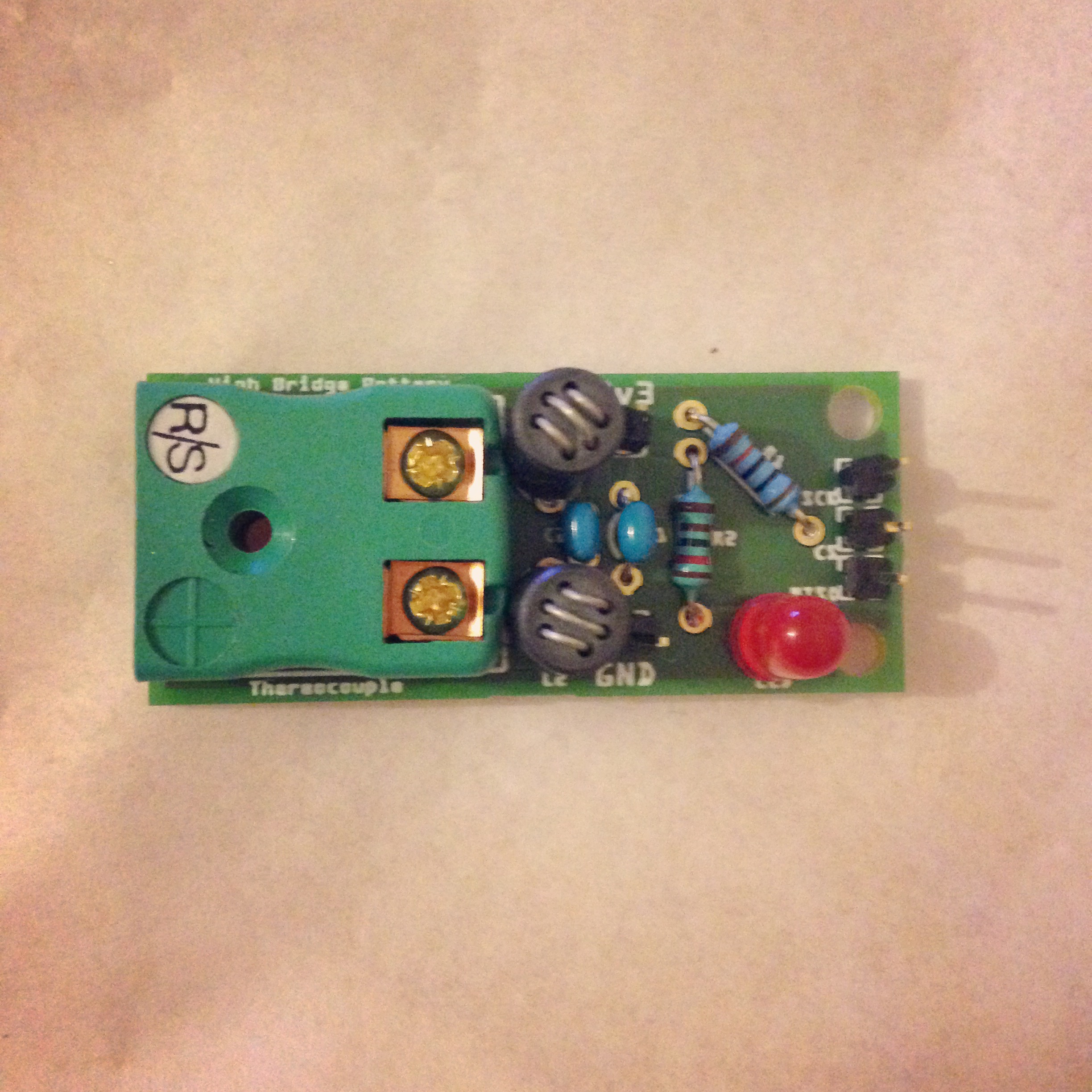
Finally made it round to sending off a PCB for print, used the fritzing fab and it worked great with my part. Longest 2 week wait of my life for the boards to be delivered. The holes were slightly over sized but the connector soldered in great.
I did get some issues with fritzing slowing down designing a board larger than this. Would lag really bad.
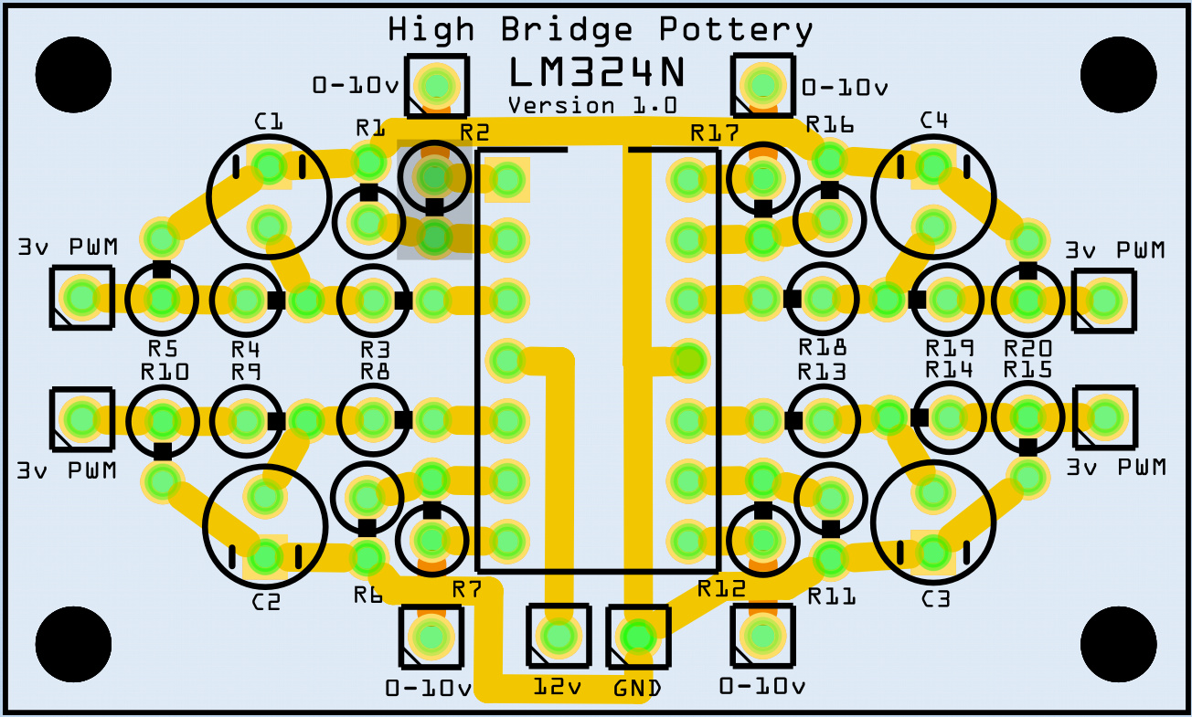
That not a terribly complex board. Can you reproduce the slow down (perhaps by increasing your grid size)? The only time I’ve seen slow graphics response in Fritzing is when I had 13 subparts for Brads education board. That slowed rendering to a crawl (and necessitated a different design). If its a grid size issue, that’s more or less normal but if its another bug of some kind knowing what it is would be useful.

 . I’d expect their web page should have a standard drill size chart, otherwise I think (remembering I don’t do boards much