The MH-CD42 Lithium battery charge/discharge module.
Please let me know if anything is wrong with the part so I can fix it.
MH-CD42.fzpz (52.2 KB)
The MH-CD42 Lithium battery charge/discharge module.
Please let me know if anything is wrong with the part so I can fix it.
MH-CD42.fzpz (52.2 KB)
There is already a part here
Exactly the same
Do look a this part creation tutorial if you have not seen it yet
As well FritzingCheckPartw.py (documented in my tutorial that @RAPTOR7762 referred to above) flags a number of errors which likely means your part doesn’t work correctly. The warnings shouldn’t usually cause problems, but the Errors indicate things that will break. If you are using Adobe Illustrator you need to us the parts editor to correct the svg files to the correct format for Fritzing (Illustrator likes to use px which doesn’t work in Fritzing.) There are posts in the forum that describe what to do.
$ FritzingCheckPartw.py part.MH-CD42_08b0863fbbd3e4ce148be50c0de4f539_7.fzp
**** Starting to process file Startup, no file yet
**** Starting to process file part.MH-CD42_08b0863fbbd3e4ce148be50c0de4f539_7.fzp
**** Starting to process file svg.breadboard.MH-CD42_5a5c00d416410032cb9f86f595ef467e_3_breadboard.svg.bak
**** Starting to process file svg.schematic.MH-CD42_5a5c00d416410032cb9f86f595ef467e_3_schematic.svg.bak
**** Starting to process file svg.pcb.MH-CD42_5a5c00d416410032cb9f86f595ef467e_3_pcb.svg.bak
File
‘part.MH-CD42_08b0863fbbd3e4ce148be50c0de4f539_7.fzp.bak’
This is a through hole part as both copper0 and copper1 views are present.
If you wanted a smd part remove the copper0 definition from line 50
Modified 4: File
‘svg.breadboard.MH-CD42_5a5c00d416410032cb9f86f595ef467e_3_breadboard.svg.bak’
At line 5
ReferenceFile
‘MH-CD42.svg’
doesn’t match input file
‘MH-CD42_5a5c00d416410032cb9f86f595ef467e_3_breadboard.svg’
Corrected
Modified 4: File
‘svg.schematic.MH-CD42_5a5c00d416410032cb9f86f595ef467e_3_schematic.svg.bak’
At line 5
ReferenceFile
‘MH-CD42 Schematic.svg’
doesn’t match input file
‘MH-CD42_5a5c00d416410032cb9f86f595ef467e_3_schematic.svg’
Corrected
Modified 4: File
‘svg.pcb.MH-CD42_5a5c00d416410032cb9f86f595ef467e_3_pcb.svg.bak’
At line 5
ReferenceFile
‘MH-CD42 PCB.svg’
doesn’t match input file
‘MH-CD42_5a5c00d416410032cb9f86f595ef467e_3_pcb.svg’
Corrected
Modified 3: File
‘svg.pcb.MH-CD42_5a5c00d416410032cb9f86f595ef467e_3_pcb.svg.bak’
At line 23
Silkscreen fill color #fff isn’t white or black. Set to black.
Modified 1: File
‘svg.pcb.MH-CD42_5a5c00d416410032cb9f86f595ef467e_3_pcb.svg.bak’
At line 39
Removed px from font-size leaving 37.5
Modified 3: File
‘svg.pcb.MH-CD42_5a5c00d416410032cb9f86f595ef467e_3_pcb.svg.bak’
At line 39
Silkscreen fill color #fff isn’t white or black. Set to black.
Warning 6: File
‘part.MH-CD42_08b0863fbbd3e4ce148be50c0de4f539_7.fzp.bak’
At line 2
ReferenceFile name
‘resistor.fzp’
Doesn’t match fzp filename
‘MH-CD42_08b0863fbbd3e4ce148be50c0de4f539_7.fzp’
Warning 11: File
‘part.MH-CD42_08b0863fbbd3e4ce148be50c0de4f539_7.fzp.bak’
At line 150
Type pad is not male (it usually should be)
Warning 14: File
‘part.MH-CD42_08b0863fbbd3e4ce148be50c0de4f539_7.fzp.bak’
At line 157
terminalId missing in schematicView (likely an error)
Warning 36: File
‘part.MH-CD42_08b0863fbbd3e4ce148be50c0de4f539_7.fzp.bak’
Connector0 doesn’t exist. Connectors should start at 0
Warning 35: File
‘part.MH-CD42_08b0863fbbd3e4ce148be50c0de4f539_7.fzp.bak’
Connector0 doesn’t exist when it must to stay in sequence
Warning 19: File
‘svg.breadboard.MH-CD42_5a5c00d416410032cb9f86f595ef467e_3_breadboard.svg.bak’
At line 3
Height 60px is defined in px
in or mm is a better option (px can cause scaling problems!)
Warning 19: File
‘svg.breadboard.MH-CD42_5a5c00d416410032cb9f86f595ef467e_3_breadboard.svg.bak’
At line 3
Width 89px is defined in px
in or mm is a better option (px can cause scaling problems!)
Warning 19: File
‘svg.schematic.MH-CD42_5a5c00d416410032cb9f86f595ef467e_3_schematic.svg.bak’
At line 3
Height 93px is defined in px
in or mm is a better option (px can cause scaling problems!)
Warning 19: File
‘svg.schematic.MH-CD42_5a5c00d416410032cb9f86f595ef467e_3_schematic.svg.bak’
At line 3
Width 57px is defined in px
in or mm is a better option (px can cause scaling problems!)
Warning 19: File
‘svg.pcb.MH-CD42_5a5c00d416410032cb9f86f595ef467e_3_pcb.svg.bak’
At line 3
Height 62px is defined in px
in or mm is a better option (px can cause scaling problems!)
Warning 19: File
‘svg.pcb.MH-CD42_5a5c00d416410032cb9f86f595ef467e_3_pcb.svg.bak’
At line 3
Width 91px is defined in px
in or mm is a better option (px can cause scaling problems!)
Warning 20: File
‘svg.pcb.MH-CD42_5a5c00d416410032cb9f86f595ef467e_3_pcb.svg.bak’
At line 57
copper1 layer should be at the top, not under group copper0
Error 88: File
‘svg.breadboard.MH-CD42_5a5c00d416410032cb9f86f595ef467e_3_breadboard.svg.bak’
At line 3
viewBox attribute missing
Error 69: File
‘svg.breadboard.MH-CD42_5a5c00d416410032cb9f86f595ef467e_3_breadboard.svg.bak’
At line 24
Found a drawing element before a layerId (or no layerId)
Error 88: File
‘svg.schematic.MH-CD42_5a5c00d416410032cb9f86f595ef467e_3_schematic.svg.bak’
At line 3
viewBox attribute missing
Error 69: File
‘svg.schematic.MH-CD42_5a5c00d416410032cb9f86f595ef467e_3_schematic.svg.bak’
At line 27
Found a drawing element before a layerId (or no layerId)
Error 88: File
‘svg.pcb.MH-CD42_5a5c00d416410032cb9f86f595ef467e_3_pcb.svg.bak’
At line 3
viewBox attribute missing
Error 74: File
‘svg.pcb.MH-CD42_5a5c00d416410032cb9f86f595ef467e_3_pcb.svg.bak’
At line 61
Connector connector6pin has no radius no hole will be generated
Error 74: File
‘svg.pcb.MH-CD42_5a5c00d416410032cb9f86f595ef467e_3_pcb.svg.bak’
At line 70
Connector connector5pin has no radius no hole will be generated
Error 74: File
‘svg.pcb.MH-CD42_5a5c00d416410032cb9f86f595ef467e_3_pcb.svg.bak’
At line 79
Connector connector4pin has no radius no hole will be generated
Error 74: File
‘svg.pcb.MH-CD42_5a5c00d416410032cb9f86f595ef467e_3_pcb.svg.bak’
At line 88
Connector connector3pin has no radius no hole will be generated
Error 74: File
‘svg.pcb.MH-CD42_5a5c00d416410032cb9f86f595ef467e_3_pcb.svg.bak’
At line 97
Connector connector2pin has no radius no hole will be generated
Error 18: File
‘part.MH-CD42_08b0863fbbd3e4ce148be50c0de4f539_7.fzp.bak’
Connector connector7pin is in the fzp file but not the svg file. (typo?)
svg svg.pcb.MH-CD42_5a5c00d416410032cb9f86f595ef467e_3_pcb.svg.bak
Peter
Hi,
thank you, haven’t found this tutorial yet bt will check it out now.
It seems to be the same part, but the solder pad for KEY is missing. I will try to fix my part as it took several hours to get it to work and I want to use the pad on my project. ![]()
Hi,
I actually used Affinity Designer, I will take a look at the Python Script and try to get it fixed. Thank you!
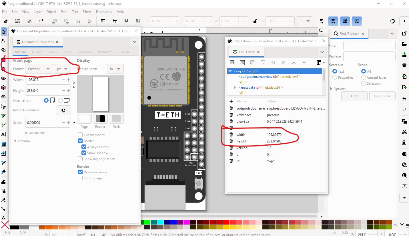
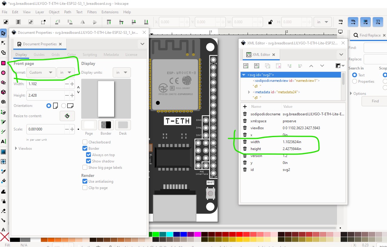
I don’t know Affinity Designer ( I use Inkscape) but what you want is from this (where the dimensions are in px because they have no dimension) and where Fritzing will guess (sometimes incorrectly) what the px to DPI conversion should be based on what it knows about the svg editor in use (I expect it doesn’t recognize Affinity Designer although that I may be wrong!)
to this which has the dimensions in inches
As well before making parts I always do a google search of the form “fritzing part MH-CD42 Lithium battery charge/discharge module” which should find the module that @RAPTOR7762 referenced. That at least gives you a place to start to modify the svgs if the part doesn’t match which makes life a lot easier. Making parts is hard and complex.
Peter
Hi Peter,
I’m aware of the unit-problem when exporting the SVG, but I have no option to change it. Inkscape ‘speaks’ SVG native, so it has some advantages besides being free. ![]()
Your python scipt really is nice, I’m fixing the errors at the moment. There seems to be a naming issue with the fonts and it seems there are some references left when using another part as starting point. Is there a way to start the part editor without using e.g. a resistor and delete all the values?
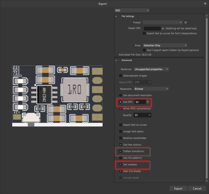
I got the dimensions right, when using 90 dpi for export the Fritzing editor shows the exact measurements I have drawn in Affinity.
Can something go wrong afterwards if the part fits this way? If that’s the case I will edit the files manually (after I fixed the other errors ![]() ).
).
Do you have an idea how to manage the solder pad on the PCB view? The pad itself is on the module and has no direct connection to the PCB. But the script wants a connector anyway. ![]()
Even if it is complex to start from scratch, I gladly loose some time to learn new stuff.
It seems I just have messed up the Google search and the forum search only shows this thread.
Best regards
Uwe
Fritzing only accepts two fonts OCRA and "droid sans’ both available for download on the Fritzing web site. FritzingCheckPart.py is somewhat incorrect as Fritzing will substitute one of the supported fonts for whatever is actually present rather than not render it.
I tend to start from a template file and ignore parts editor entirely (as noted in the tutorial.) with enough experience (I have been making parts for 8 or 9 years now) it gets fairly easy to fix things up manually. Parts editor (which was not complete when development stopped in 2016, and AFAIK hasn’t been finished yet after development restarted) and thus has enough limitations one of which is requiring you to start from a part with the correct number of pins defined for the part you want to make. It can’t change the number of pins or sometimes modify the fzp file (which is required to change the number of pins) except in a limited way.
That is likely because 90DPI is what Inkscape was using around 2016 (today it is using 96DPI, I think because of a svg standard change) so that should do fine. Fritzing is guessing that this is Inkscape and I believe will change the dimensions to inches when it writes the svg so all should then be well. That is the solution for Adobe illustrator as well, importing it to the parts editor (with its default 72dpi setting) will write out inch dimensioned svgs which then work fine in Inkscape so all should be well (except that you have to deal with parts editor which I don’t want to, I find editing the files to be much easier ![]() ) I have a bunch of still fairly rough python scripts that make part making much easier, but few enough people learn to make parts that I haven’t cleaned them up enough to publicly release but I will send them to you via PM if you like. You may occasionally have to modify the python to do what you want and you generally have to manually edit the files with a text editor to insert the boiler plate code then add the description fields (and format the svgs correctly with all connectors at the very bottom where the tools expect to find them.)
) I have a bunch of still fairly rough python scripts that make part making much easier, but few enough people learn to make parts that I haven’t cleaned them up enough to publicly release but I will send them to you via PM if you like. You may occasionally have to modify the python to do what you want and you generally have to manually edit the files with a text editor to insert the boiler plate code then add the description fields (and format the svgs correctly with all connectors at the very bottom where the tools expect to find them.)
Peter
@wuergezwerg just a word of caution don’t use new part editor for this part.
Follow the instructions below
In this case, it would be the “key” pad. Also not that connectors start with “connector0pin” and not “connector1pin”
Hope this helps
Always happy to answer questions regarding fritzing parts. We are short of part makers (6 part makers are now MIA)
Edit:
Peter mentioned the parts editor has not been completed. This is true (based on experience. I still use part editor to make parts faster, but when it comes to suppressing PCB view, I edit .fzp file) You can’t have undefined connectors as everything is predefined. The only way to change it is to edit the .fzp file
It is also preferable to use the Inkscape extension (reliable and fast)
Thank you for all your tips!
Even if Inkscape is the prefered software, I will try creating a template in Affinity Designer (really like this software ![]() ). There are also some options to simplify the SVG files which look promising. I used the fonts from the Fritzing homepage, but after the export it adds some additional information and Fritzing does not recognize it this way.
). There are also some options to simplify the SVG files which look promising. I used the fonts from the Fritzing homepage, but after the export it adds some additional information and Fritzing does not recognize it this way.
![]()
Is there a documentation for the allowed XML tags?
@vanepp: I really like to take a look at your scripts, it shouldn’t be too difficult to adapt them to my needs.
Not that I am aware of. Documentation in general is lacking, most of what we know has been passed down from people experimenting. The developers may have some more and can look at the code to see what it will object to. Opening an issue on github here
would be your best bet I expect (they may or may not respond as they are pretty busy with development issues. I expect what Fritzing is objecting to is the multiple font family names (probably especially the sans-serif part) that is probably tripping the invalid font family code in Fritzing at a guess. The source is available on github if not easy to deal with.
I’ll send them to you in a pm in a while.
Peter
The best information is that Fritzing uses the “small svg” standard (I think that is the right name). For the extra font information, one of the options to ‘simplify’ the svg output might fix that. A lot can be done with careful selection of export options in Inkscape. Affinity might do the same.