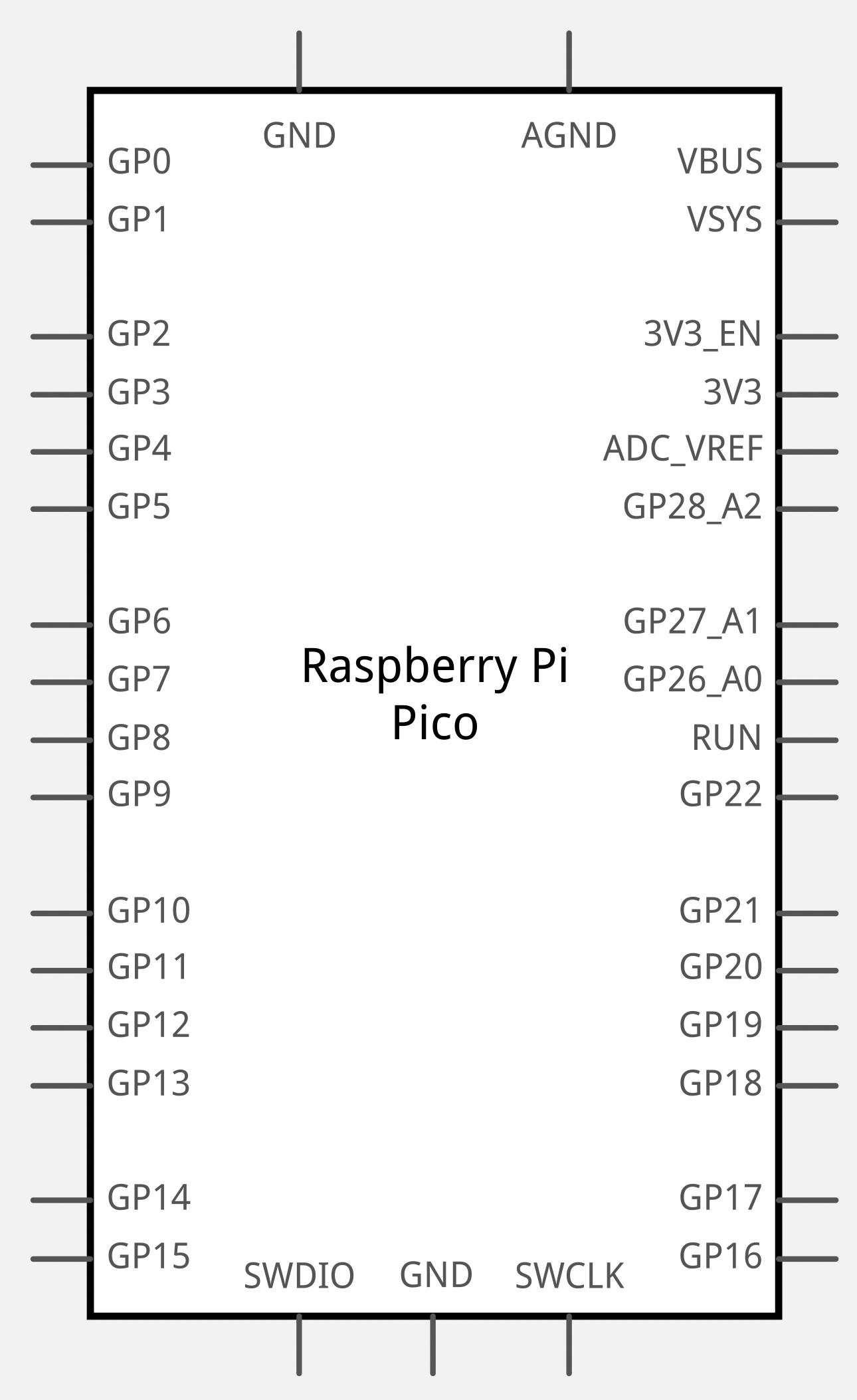
The dimension is at https://www.cytron.io/p-raspberry-pi-pico-pre-soldered-headers
I don’t have it on-hand to verify that the dimension given is correct.
There is a part of sorts available here:
https://www.raspberrypi.org/documentation/pico/getting-started/
in the board specifications section as download Fritzing part. It has a fair number of problems though, it lacks terminalIds in schematic (which will cause the connection to be in the middle of the pin rather than the end), appears to have no layerIds (and thus won’t export as an svg from a sketch), and (most importantly) paths for the connectors in the pcb svg which will not generate holes in the gerber output (thus your pcb will have no holes which is probably undesirable!) At a quick look at the existing part, I think starting again from scratch is going to be the easiest solution (there is some kind of odd Illustrator binary format in the svgs apparently called a pgf which does not appear to be xml (although Fritzing appears to deal with it.) I’ll probably make a correct part, but it may take a few days (I may even try and find a way to offer it to the RPI folks  if I can figure out how to contact them!) The current part would only be useful in breadboard and schematic views (if you connect straight in to the lines, the lack of terminalIds won’t matter) I expect, pcb view generates no holes (although the pads are there) and therefore likely won’t be useful.
Peter
Thank vanepp, Raspberry Pi fritzing part is no holes indeed. Also, when I use ZofzPCB 3D viewer to open Gerber, there are a few errors shown. So, It will be best to wait for your new design. 
Turned out to be easier than I thought. Ungrouping in Inkscape and then deleting the unknown Illustrator node gave me a conventional (if still wrong and incorrect scale ) set of svgs. Adjusted those to meet Fritzing graphics standard and added circles to pcb (and a silkscreen which it lacked) to make a corrected part (also a lot smaller one, 24K vs 648K) :
edit: Replaced this part with 2 new ones below! If you downloaded this one, you want to update!
As I assume you have an actual board, please print out the footprint and verify it against an actual board (I assumed the original part was correct which it may not be!) Note by default the mounting holes in pcb are not drilled. To drill them you need to drag a hole from core parts/pcb in to the sketch and position it over the hole in silkscreen on the part (you can add the hole if you want it but can’t remove one without modifying the part!) Checking their position is correct would be helpful.
Peter
That is a bit map image embedded inside the svg. At least I assume you meant the I:aipgf elements. Progressive Graphics File - Wikipedia
If I read that right, the associated switch and foreignObject elements says to use one or the other. I’ve never looked at the switch element, but that is what the structure implies.
I see that the original breadboard svg included silkscreen and copper 0 layers, but NOT a breadboard layer.
That makes sense. They may have used it (as I sometimes do) to place the components, and then not deleted it. There is a brd file, but Eagle can’t open it (I seem to recall the PI folks may use altium rather than Eagle) so I have to assume they got the board layout right (which seems a good bet since the pin spacing looks correct.)
Peter
Hello @vanepp,
Thank you for making the changes. I was using the original part (without the faintest clue about the challenges down the road if uncorrected) but will now upgrade to yours. Given the nature of Pico and its use cases, I’m sure that many folks will definitely want to avail this update.
Kind regards.
Hey all,
I’m in charge of the Raspberry Pi documentation, and the person that built the official part. First part I’ve ever done, so I’m not that unhappy with it. The absence of holes for the gerber is sort of a choice, as the board is castellated we’re expecting people to solder it onto PCBs rather than attach it through hole?
I’m happy to take contributions (or replacement parts) so long as you’r happy to release the part under the right licensing terms.
That said I took a look and it looks like your Pico part has connections between GP10 and GP21 and GP11 and GP20. The pins are linked in the schematic view?
Cheers,
Alasdair
Welcome aboard!
Over all a nice job, the lack of holes in pcb was the major issue, the rest are fairly minor (although the lack of a layerID in breadboard means that if exported from a sketch as an svg, the part won’t appear!) I have a python script that will find various such errors in a part available here:
which will flag errors (that’s what alerted me to no holes) and change some things (remove px from font size which you looked to have done, and inline style commands) that Fritzing doesn’t support. Although I’m not all that familiar with castellatization I don’t think the hole should prevent soldering the module to the board, while leaving the user the option of installing .1in headers to plug the module in if they wish. If you disagree, it is easy enough to remove the pads I added that create the holes and move the connectorIds back to the paths. Fritzing PCB view shows holes for through hole pads even when they are not in the gerbers (and therefore the board.) There have been more than one case with incorrectly configured parts where users have had boards made only to discover they are useless because of no holes, so I would lean towards leaving the holes if they won’t case a problem with soldering the board.
As far as I know parts are released under the Creative Commons share alike license (Fritzing itself is gpl), in any case I’m good with sharing (as the part is mostly yours anyway ![]() ) While I’m here there is a RPI 4B part available here that you are welcome to as well:
) While I’m here there is a RPI 4B part available here that you are welcome to as well:
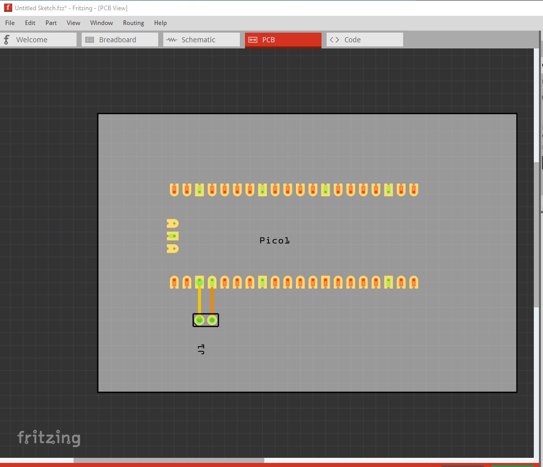
They don’t appear to be to me. The grounds are all linked:

but the gpio is not (the other pin should light yellow when left clicked on if they are connected to each other internally or by an external wire.)
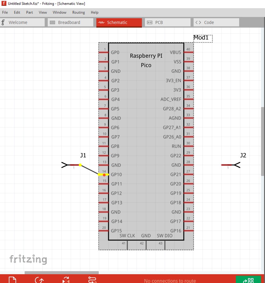
I did change the internal pin number order to start the internal pins at pin0 and pin0 as pin1 on the module (aligned as if it was an IC), but that shouldn’t affect this. The above image reminds me of one other error, on your part schematic doesn’t have terminalIds defined and thus if you connect a wire as I did here at a 45 degree angle, the connection is to the middle of the pin rather than to the end as is desirable. In this case the terminalId is a 10thou by 10thou rectangle positioned on the end of the pin.
Peter
Although I’m not all that familiar with castellatization I don’t think the hole should prevent soldering the module to the board, while leaving the user the option of installing .1in headers to plug the module in if they wish.
You’re probably right. More on Castellated Modules at How to Solder: Castellated Mounting Holes - SparkFun Learn. Which is a good introduction on what they’re for and how to solder them.
As far as I know parts are released under the Creative Commons share alike license
We’re being a bit more aggressive on licensing. We’re releasing KiCAD design files (and the Fritzing part) wit permission to use, copy, modify, and/or distribute for any purpose with or without fee. So, entirely openly in other words.
Would you be happy for your part to be released under a similar license?
While I’m here there is a RPI 4B part available here that you are welcome to as well
Many thanks! Similar license question there I guess?
That said I took a look and it looks like your Pico part has connections between GP10 and GP21 and GP11 and GP20. The pins are linked in the schematic view?
They don’t appear to be to me.
Nor to me any more. Huh. Wonder what was going on. Ignore me, nothing to see there!
Cheers,
Al.
Sure I’m good with that too. I want folks to be able to use the parts!
Peter
Having looked at the Sparkfun tutorial, I think the pcb layout needs to change. It looks to me like they expect the pad for the Castellation to extend beyond the edge of the pico pcb (like a SMD IC footprint) and I think (not having the actual board) the current layout matches the module exactly, and thus needs the pads to be a bit further out to allow soldering to the half circle as in the tutorial. The board files being Kicad also explains why Eagle couldn’t read them (there is an Eagle2Fritzing program that will create Fritzing parts from Eagle files that I tried.) I’ll change pcb that way. Having the hole available on the next pad in shouldn’t affect the Castellated pad. I was concerned that the hole may not leave enough pad area for a good joint, but it looks like that should be in the pad extending beyond the module edge. I’ll post a modified part in a while.
Peter
The usual cause is a connection (or previous connection) on one of the other views. There seems to be (have not been able to reproduce on demand) a bug where creating and deleting connection wires in multiple views can end up leaving ghost wires. The problem has not been seen if connections are only created in a single view, then the rats nest wires used (turned real) in other views, instead of creating new connections.
OK, I just deleted my part above to replace it with two new ones, one SMD and one through hole:
edit: Replaced these two with new versions at the bottom of the thread!
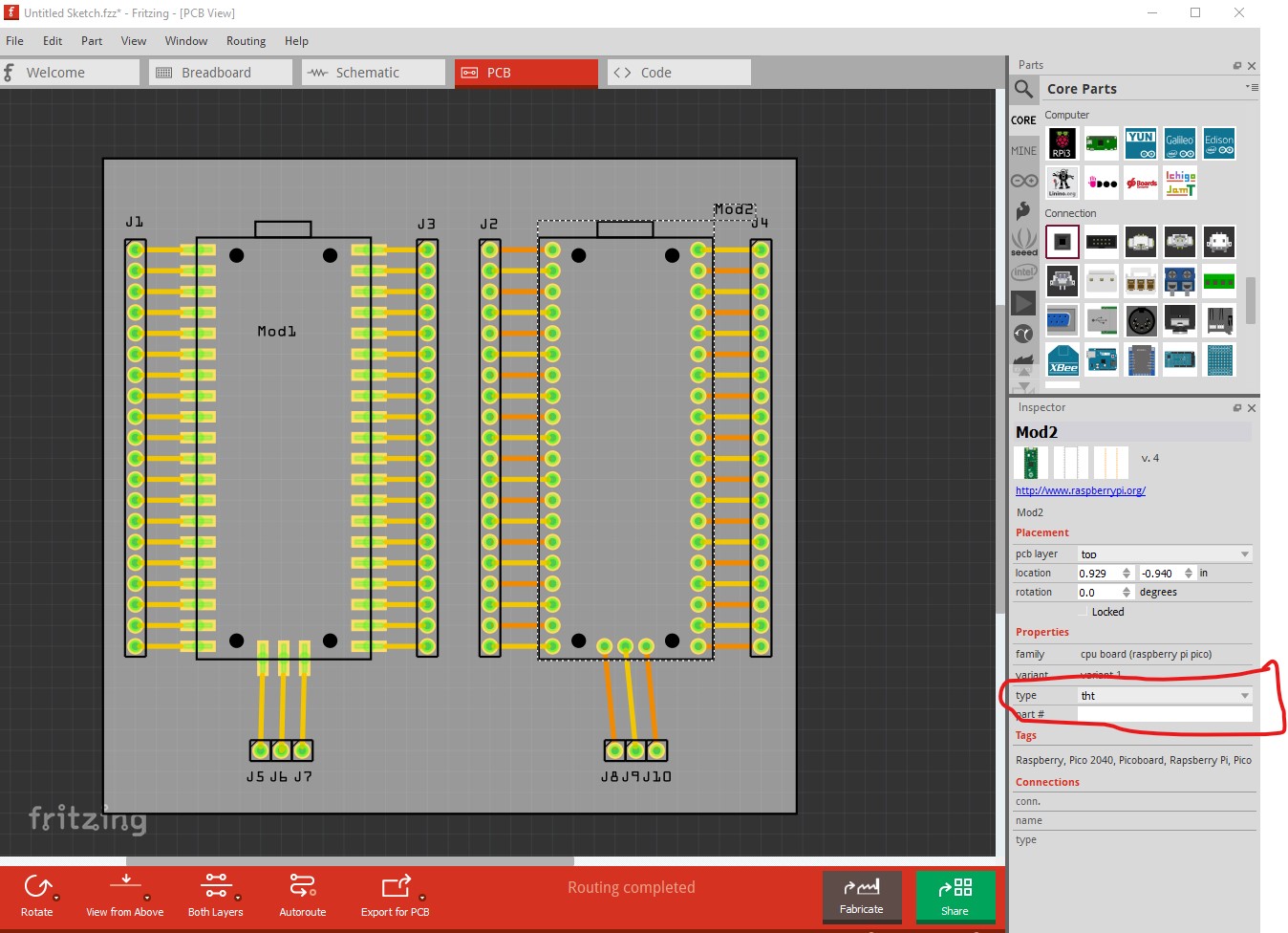
The original part (and my first one) are through hole, for the castellated mounting holes we want a SMD part. The original parts will have pads on both sides of the board (and Fritzing will happily connect to the pads on the bottom of the board which don’t connect to anything!), believing they are through hole and will connect to the pad on the top. With the smd version it knows the pads are only on the top layer (or the bottom if pcb layer is set to bottom.) It is also possible to have one pico on the top of the board and by setting pcb layer in Inspector from top to bottom, have another independent pico on the bottom of the board in the same place. Here is a test sketch with the tht (on the right) board selected. To change to the smd board, set type (circled in red in the Inspector window in the lower right window) to smd and it will switch to the smd version. Doing this with wires connected, as in this sketch screws up though, so you need to disconnect the traces before doing it. If you only want to support one part, and use the castellated mounting holes then you want the smd part as it is the only one that will work correctly in that case.
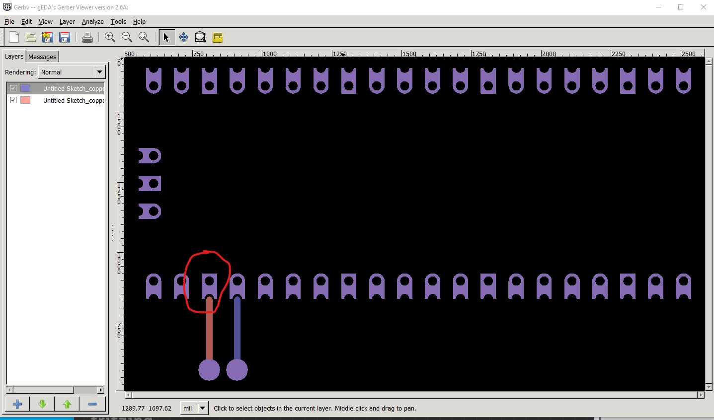
To see the difference between the two, we need to switch to the gerber output (using gerbv in this case), first with the layers copper bottom, copper top, drill and silkscreen top selected:
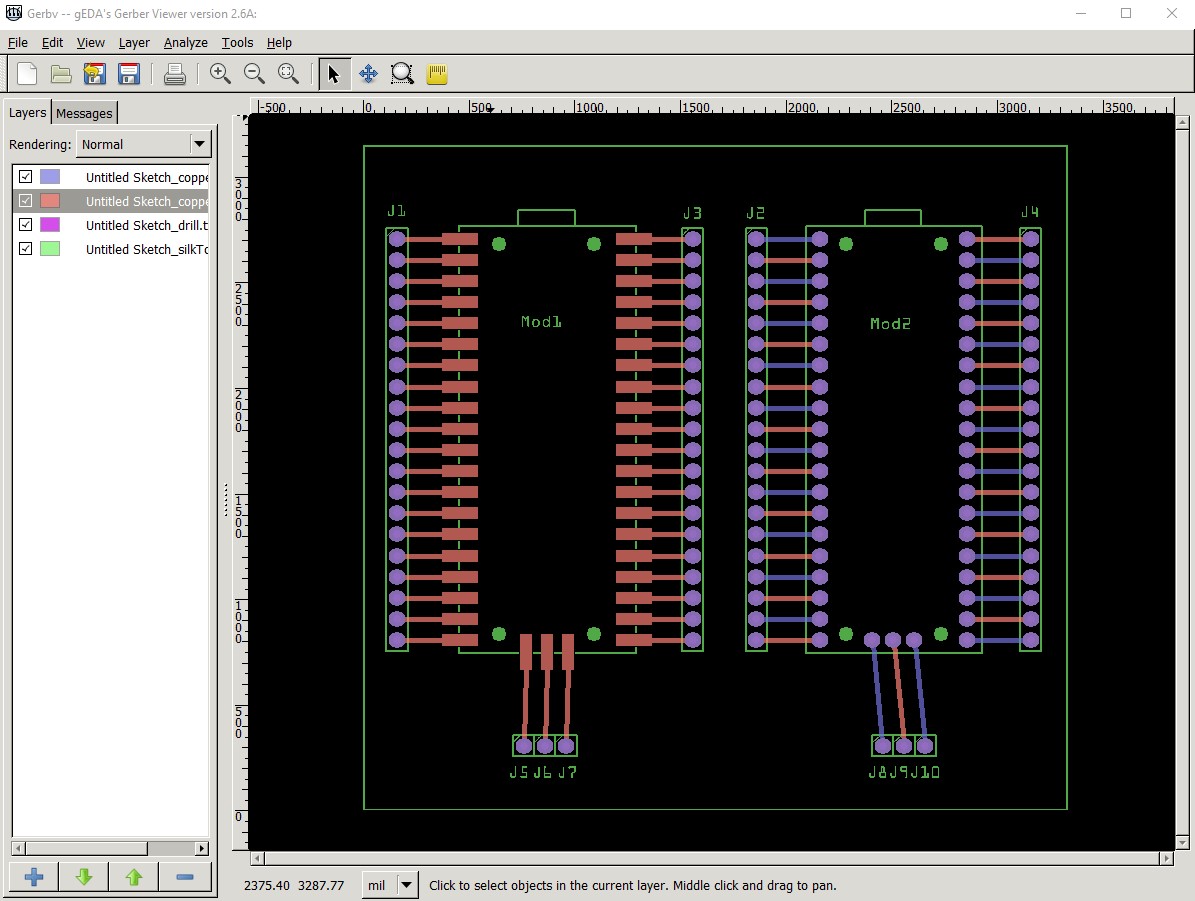
other than all the traces on the top on the smd version, hard to see much difference, but when I disable the copper top layer the difference becomes obvious:
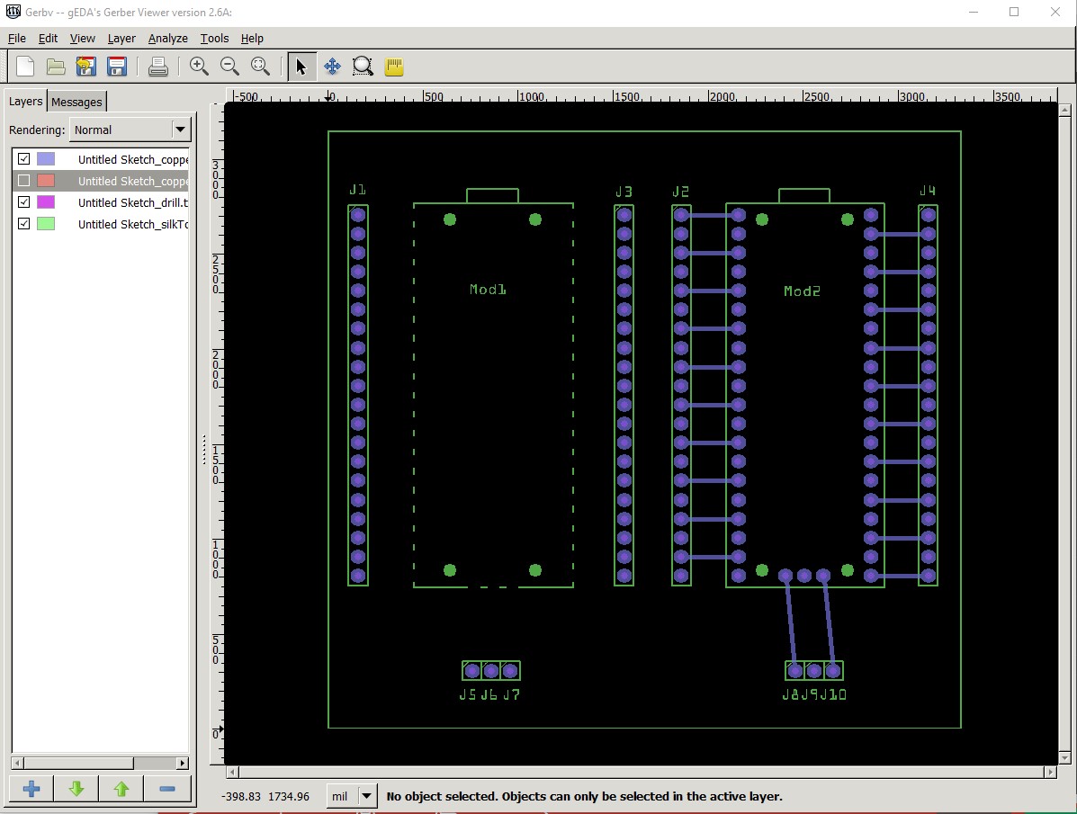
other than the .1in headers (which are through hole), there is no copper from the pico on the bottom layer and thus I could put a second instance of a pico under the one on the top (and Fritizing won’t try and connect traces on the bottom with the expectation the pad is through hole as it will in the original 2 parts!) It would be a good bet to make a board from the smd version of the part and solder a pico on to the board to make sure I have gotten the pads correct (I think they probably are, but verifying with an actual board is the only sure test!)
Peter
Hey! These parts look great. Serious improvement on my original.
I passed your comments on to the designer of the Pico and have a couple of follow ups.
If you look at the hardware design book you’ll see discussion of the VGA carrier board. There’s also good discussion about the overall Pico design there that might be helpful.
-
Why is it necessary to use multiple footprints, why not a single footprint as per the VGA board KiCAD? This has both through hole and extended pads on the board so the Pico can either be soldered down onto the board using the castellations, or attached via headers throughhole. We’d suggest that this is how most PCBs should be configured if you’re going to solder a Pico to it as a module.
-
There’s also some additional holes and copper keepouts that were specified on the VGA board, for things like where the USB pins protrude through the underside of the board, and are slightly raised, and where there are test points on the underside which we want to completely eliminate the chance of them shorting.
KiCad files are available for the VGA board if that’s helpful on the footprint side of things for either of these points.
Cheers,
Al.
Oh, one other point. Something I saw on SparkFun and Adafruit parts, but couldn’t replicate myself on ours, was consolidating the GND pins down to a single pin on the schematic (well apart from the AGND and the SWD ground).
How do you do this anyway?
Cheers,
Al.
As long as the holes are present (which they are not on the original part), that will work fine. As I set out to demonstrate this I found another problem as well (which is a Fritzing quirk) the traces don’t connect to the pad in the gerber output. Here is your original part with a 2 pin header with one trace on the top of the board and another on the bottom. To Fritzing this is fine as it thinks there is a plated through hole in the pad (but there isn’t!)
Here is the gerber output generated by the above pcb view which shows the problems:
First (the Fritzing quirk) that trace is not connecting to the pad correctly presumably because Fritzing thinks the end of the pad is square which it isn’t. Because the gerber output is done after pcb view is rendered, it is possible, as in this case, to have unexpected errors that don’t show up unless you check the gerber output from Fritzing with a gerber viewer (which many new comers don’t know to do!) The other problem is that if you solder the Pico on the top of the board in this case the connection on the bottom of the board (because there is no hole in the pad) will not connect to the pico (even if the pad was properly connected!) As well the pads all appear on the bottom of the board as well when they only need to appear on the top of the board to solder the Pico in using the castellations, that means there is much more room for routing traces on the bottom of the board (and as noted, it is also possible to mount another independed Pico on the bottom of the board if you had a reason to do so.) With the Fritzing SMD part, Fritzing is aware there are only pads on one side of the board and thus won’t allow you to make a connection on the bottom of the board. You can certainly make a single footprint board by just making sure there are plated through holes and I can modify the tht footprint to do both if you like by simply adding the pads from the smd part to the tht part so you can do either, but the smd part is more flexible and thus worth keeping I think.
I can add the 4 USB holes (non plated through) and the keepout areas in silkscreen on pcb easily enough, I didn’t know they were there previously.
This one is fairly easy (and I should do it), you just overlay the pins on top of one another. The pins all need to be present, but as long as they are in a bus they will connect together correctly (if they aren’t in a bus, problems occur though!) That is actually usually a good idea as Fritzing only allows a single connection in schematic between two buses, and if you have two Picos for instance and connect a wire between the grounds, you can’t make a connection to a second ground pin between the 2 parts and that confuses new users. I’ll make these changes in the parts (add the SMD pads to the tht part and add the keepouts and holes and fix up schematic.) and repost them.
Peter
That’d be great. I think we’d rather offer a single part.
I’ll make these changes in the parts (add the SMD pads to the tht part and add the keepouts and holes and fix up schematic.) and repost them.
Many thanks!
Cheers,
Al.
OK, here are two new parts with the changes made. You folks will want the tht version, as it has both holes for .1in headers and pads to allow soldering the module to the top of the board. As well the holes for the USB connector are automatically drilled and the pcb silkscreen has the keepout areas specified. Schematic has the ground pins consolidated on a single ground pin at the bottom.
edit: 25 Aug 2021: Someone pointed out (at the bottom of this thread) that export as a pdf for home etching doesn’t have center holes. So I changed the rectangle in to a path in order to make the part more complete in that the pdf output for home etching now has a hole in the center of the pad (and gerber works the same as it did before.)
Raspberry-Pi-Pico-tht.fzpz (23.2 KB)
I`ll leave the SMD part here in case anyone wants a real SMD part later (same changes as the tht part!)
Raspberry-Pi-Pico-smd.fzpz (22.5 KB)
Peter
6 Likes
Many thanks. I’ll get the new part substituted for the existing part on the Raspberry Pi sites.
Al.