Thank you so much @vanepp! super helpful  using this one for a circuit design to make a photography turn table how to video on YouTube
  much appreciated!
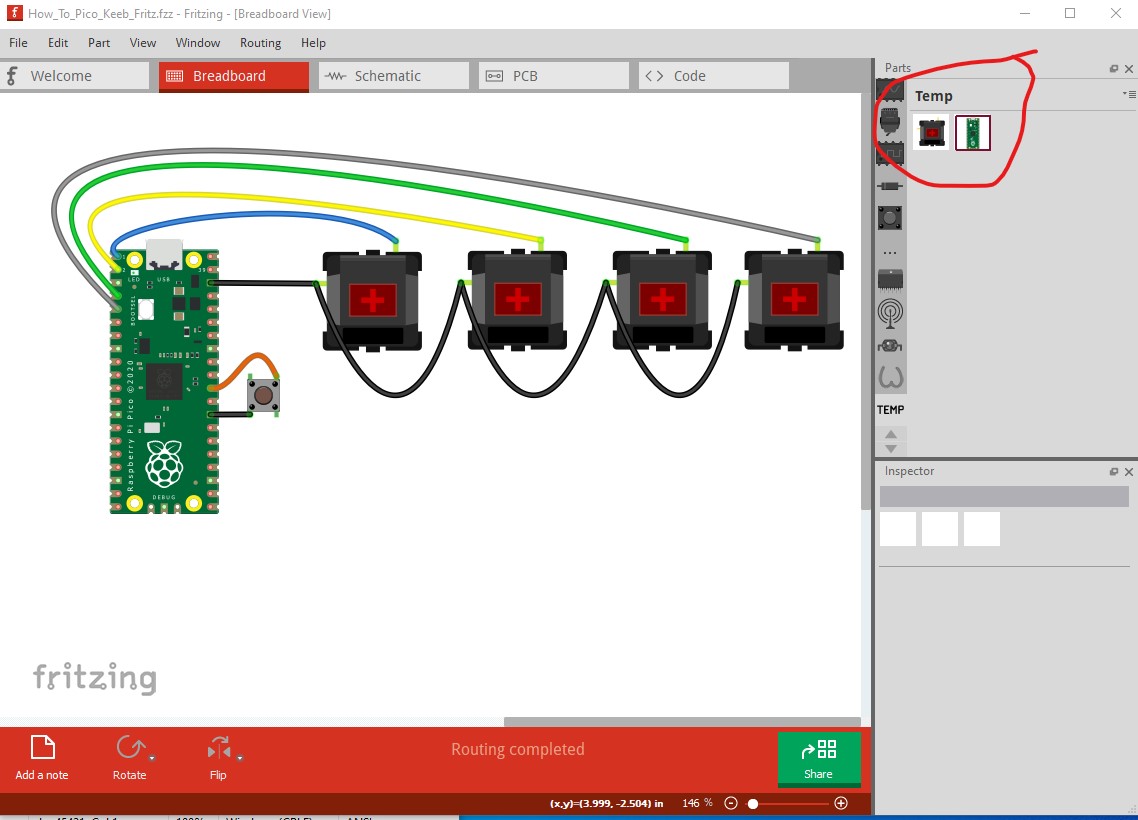
This is terrific @vanepp thanks so much – I’m using the SMD part in a mech keyboard design right this very moment!
While I think the footprint is correct (it was copied from the footprint the RPI folks used in their VGA card) it is safest to print the pcb out at 1:1 scale and check it against a real part as I don’ t have one before ordering boards.
Peter
Thanks, I did print it for scale and it all lines up great.
-John
Hi @vanepp a quick follow up, the part worked perfectly for the PCBs I had made. I wrote up a guide on using Fritzing to make a Pico mechanical keyboard here. https://learn.adafruit.com/diy-pico-mechanical-keyboard-with-fritzing-circuitpython/overview
Also, huge thanks to you for your series on Fritzing part creation, it helped me a lot in figuring out how to revise the Cherry MX keyswitch part.
1 Like
The guide looks very good! One minor nit, you don’t need to preload the custom parts
“You can download the full Fritzing file here, just make sure you’ve already imported the Cherry MX part and the Pico part”
The .fzz file includes the two custom parts and will load them automatically in the temp parts bin:
As long as the mine parts bin is in the same part as the temp parts bin there shouldn’t be a problem, but different parts can cause a problem if Fritzing uses the wrong one (Fritzing may prefer the mine parts bin over temp I think!) I ran in to this once when someone had different versions of the part in the mine and temp parts bins.
Peter
Oh, great tip, thank you! I’ll update the guide.
Hello, I have used the tht piece but when generating the pdf I do not see holes for the beak, I am not sure if the holes are made when generating the gerber. The swd pins for a tht mount I think are not necessary, could you verify it and if necessary correct it please?
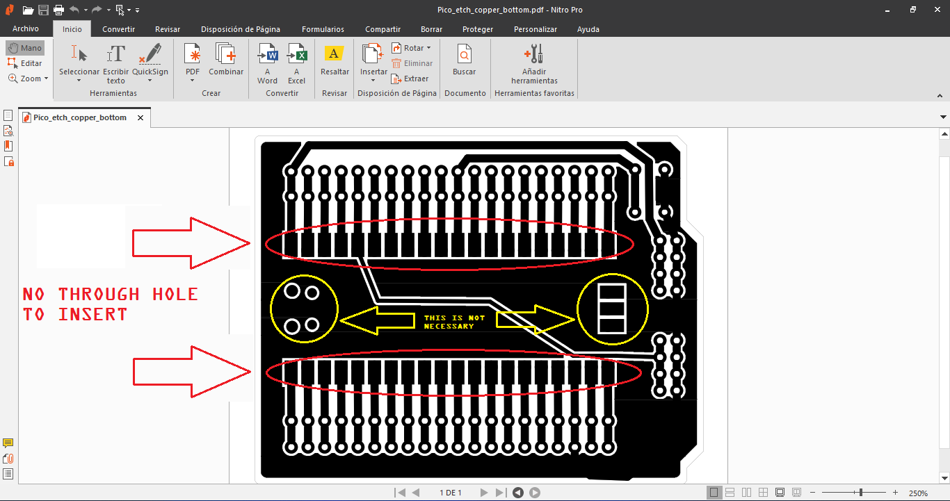
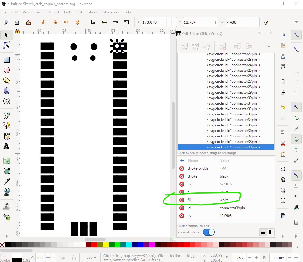
Correct. The holes are specified in the pcb svg as having fill #ffffff (which is white) but it appears on pdf etchable (PDF) the copper pad overwrites the white hole and the entire pad is black. They export correctly on the gerbers but I don’t see any way to fix this (other than converting all the pads to a path with a hole which I am probably too lazy to do, as it may not work anyway if the fills are being converted to black!) A workaround is to export as etchable svg and then edit the resulting svgs for copper bottom and copper top to change the fill back to white which it was originally like this:
current:
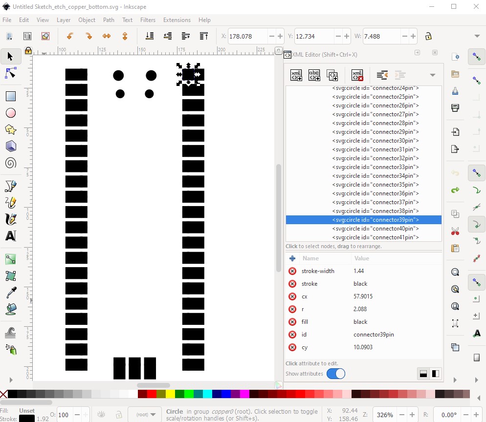
fixed, but needs to be done for all the other pins as well though, so probably a text editor on the svg is a better bet than Inkscape. The pins are all at the bottom of the svg so a global replace of fill=“black” with fill=“white” would be the most efficient way of doing this. This is basically an odd case where they wanted both through-hole and SMD in the same footprint and it looks to have run in to a Fritzing limitation.
then print the svg to get the image that you need (I don’t know how to make this change in the .pdf files, perhaps you or someone else here does!)
Peter
ok, no problem, what is really important is that when making the pcb there are effectively tht holes for the pico.
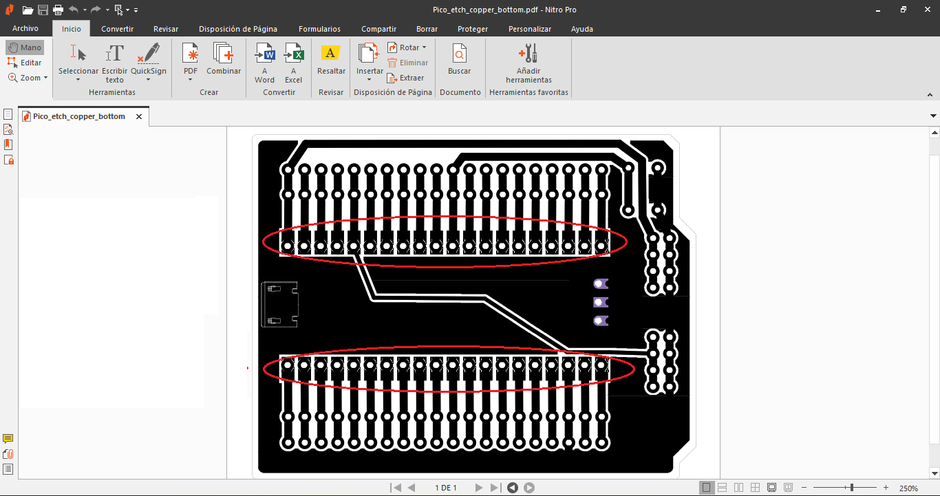
Turns out with some changes and a path in stead of the rectangle it is possible to get what you want and make this a much more complete part (usable in both gerber and home etch formats!):

the holes top clear the USB connector pins don’t have a center, but if I add one it will screw up the gerber output (by putting an undesirable copper ring around the hole) so I left it as is. I’ll replace the .tht part in the post above with the new part in a few minutes.
Peter
 Thank you so much.
add labels to the pico in breadboard view:
Pico-breadboard.fzz (70.2 KB)
Hello!
Older topic, but new (and hopefully not too stupid) question. I’ve been using the Fritzing Pico component (happily) for a while now, but recently ran into a problem. I use the Pico as an SMD component on top of a carrier board that I design.
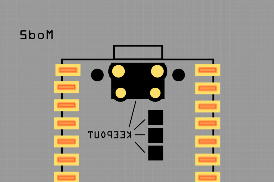
The four “circles” (for lack of precise Gerber terminology) on the underside of the USB connector result in drills in my carrier board. At first I didn’t care about these, but now I need to use this space on the underside of my carrier board.
Is there a hack to get rid of the drills? Are they actually necessary? I don’t see them being filled by anything (such as some pins going down from the USB connector).
Best regards
Joerg
Easy enough to do (although it needs a new part) but perhaps not wise. I put the holes in because the original part from the Raspberry PI folks indicated this was a keepout area and had the holes drilled (I assumed, as I don’t have a board that the pins from the USB stuck down.) It may also be that running traces under the USB will affect the USB 3 signalling, but if this works for you, this part doesn’t have the holes in the USB area.
Raspberry-Pi-Pico-smd-noUSB-holes.fzpz (22.7 KB)
Peter
Thanks a lot for the modified part, Peter! I see your point regarding interfering with USB. I only want to put my power line plus a switch there, so there will hopefully be no interference. I’ll simply give it a try with my next revision of the board. One other stupid question, though: What is the most efficient way to update the component in my schematic without losing half of the existing work including the hand-crafted layout? The menu entry “update selected components” sounds promising, but stays grayed out.
The only stupid question is the one you don’t ask ![]() . In this case what you want is delete minus. It is an option in the right click on a part menu which deletes the parts but leaves all the wires connecting to it in place. When you place the replacement part you then need to select the end of each wire and move it away from the part and then back to trigger the connection again (which is sometimes a PITA when there are traces on both sides of a connection) but better than having to redo all the traces.
. In this case what you want is delete minus. It is an option in the right click on a part menu which deletes the parts but leaves all the wires connecting to it in place. When you place the replacement part you then need to select the end of each wire and move it away from the part and then back to trigger the connection again (which is sometimes a PITA when there are traces on both sides of a connection) but better than having to redo all the traces.
Peter
If there are problems selecting/moving/reconnecting the wires/traces, you could try this sequence:
- delete minus
- move wire/trace ends away
- place new part version
- move wire/trace ends back to connect
Moving away first means it might be easier to select and move back, without issues about selecting the 'correct` trace.
Thanks, Peter and microMerlin! I’ll do as suggested.
Not sure how common my use case is, but an automated “replace part by another with same number of connectors” could be a useful feature in the future. But this is a different topic.
Cheers & a good weekend everyone!
Joerg