Hi where can you find this latching relay?
Had an attempt at it (Edit format fixed)
DFR0996.fzpz (37.5 KB)
You posted the part in wrong format. However, I’m in the process of making one
1 Like
I don’t know what that means?
Basically the file meeds to be a .fzpz file. As I said, I’m in the process of making one
1 Like
That’s fine but how do I generate the .fzpz file
1 Like
Fixed the link does it work?
1 Like
Wow! Not bad on your first try! However, here are some pointers:
Breadboard
The wire terminates to the centre (where it should not!)
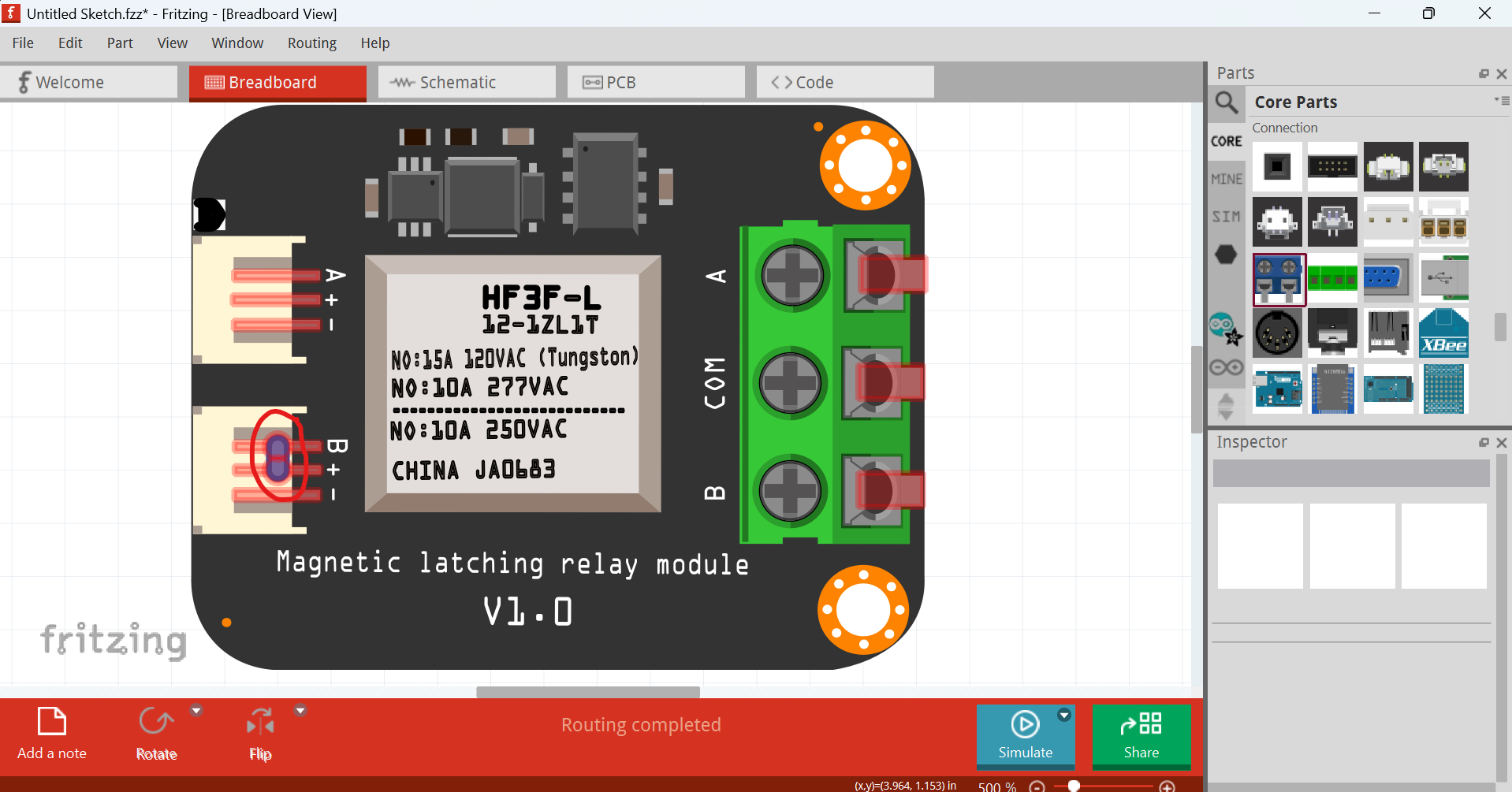
I have changed the graphic

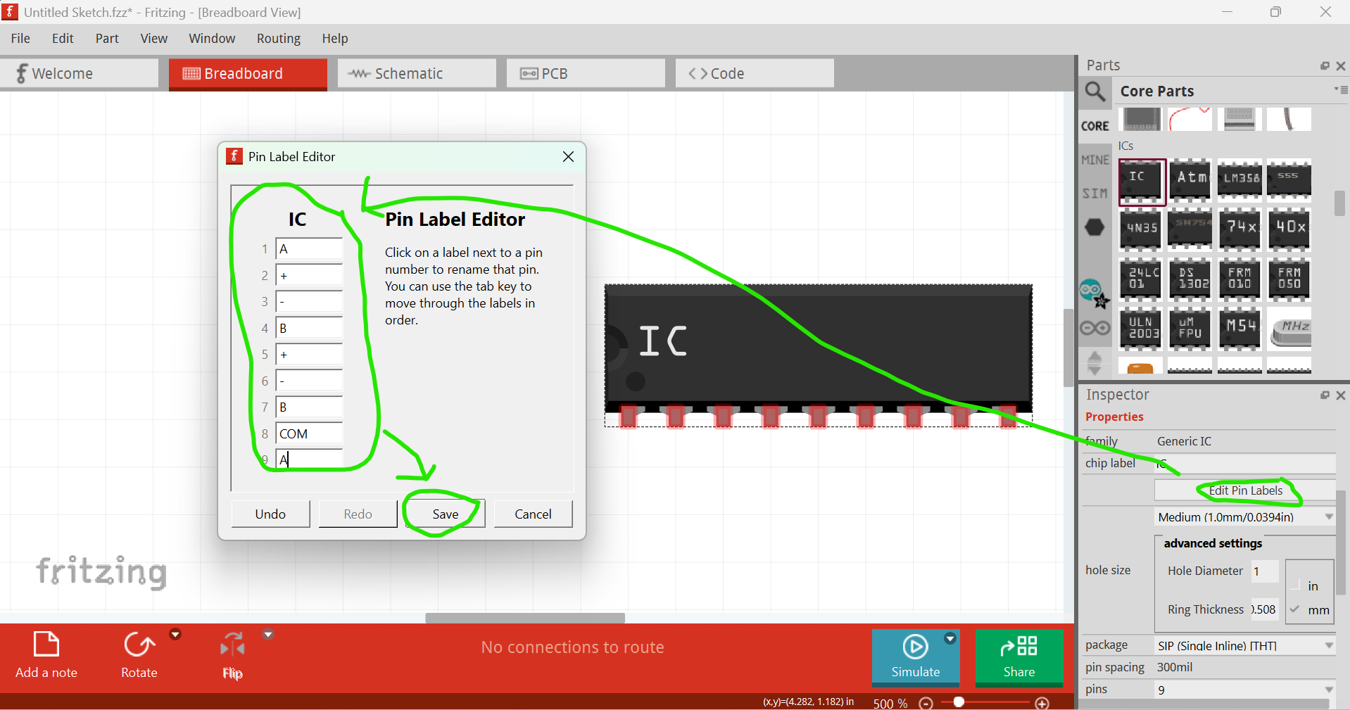
Then, the easiest way to fix the part is to start with a generic IC
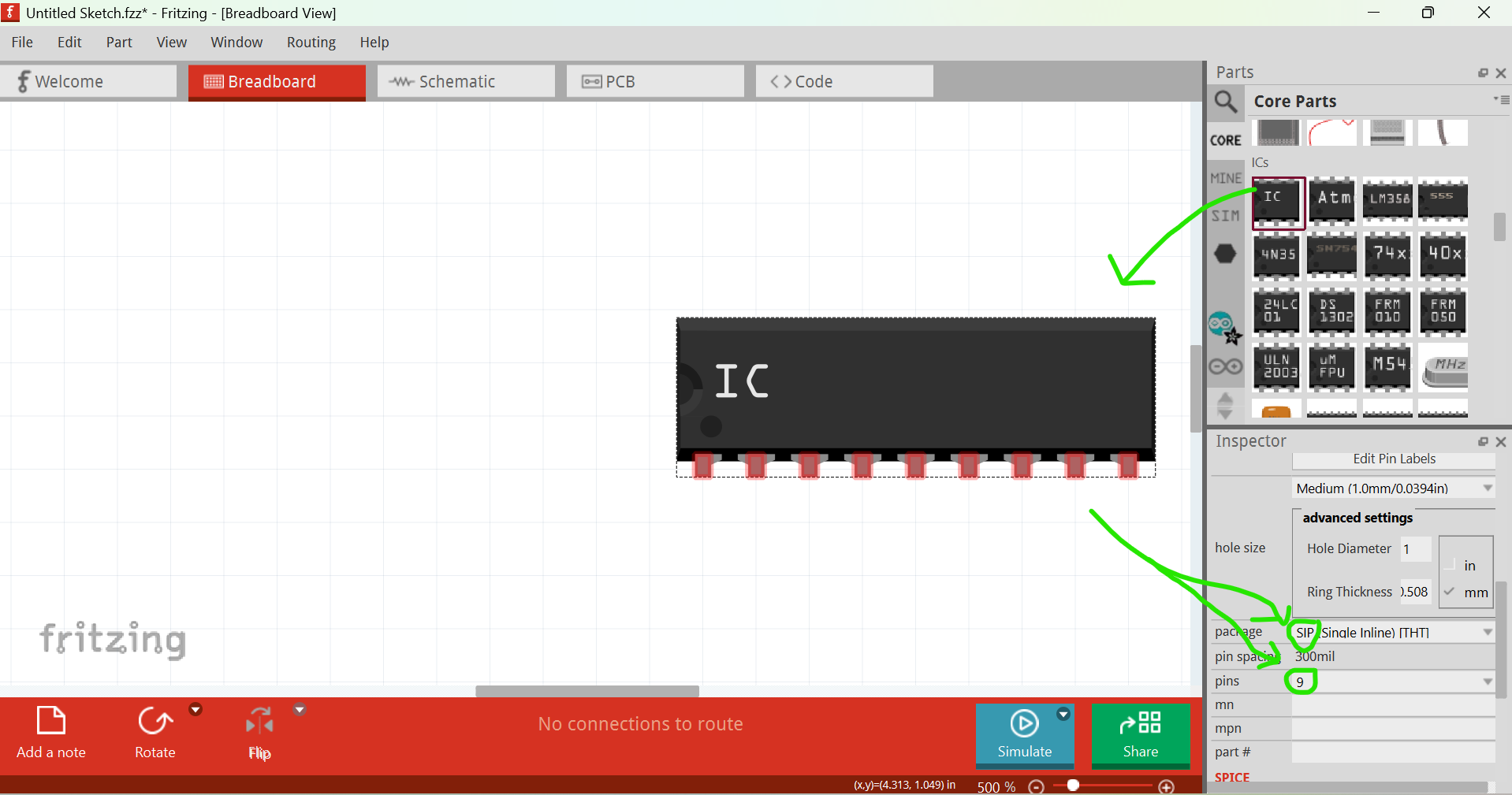
Then edit pin labels
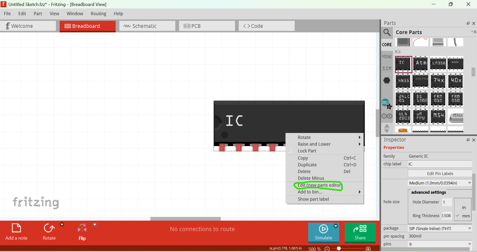
and edit part (right-click on the part in the sketch)
Then file → Load image for view (with the correctrd pin labels)
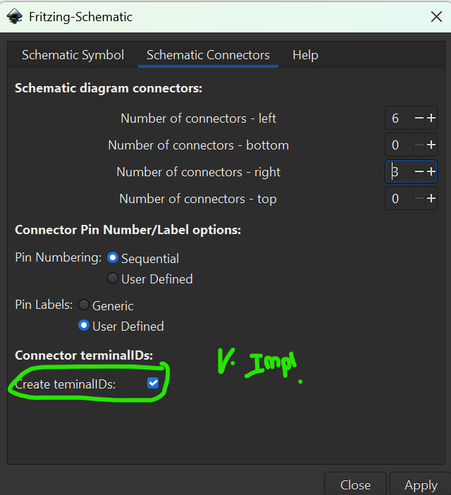
The pin order must be like this
Schematic
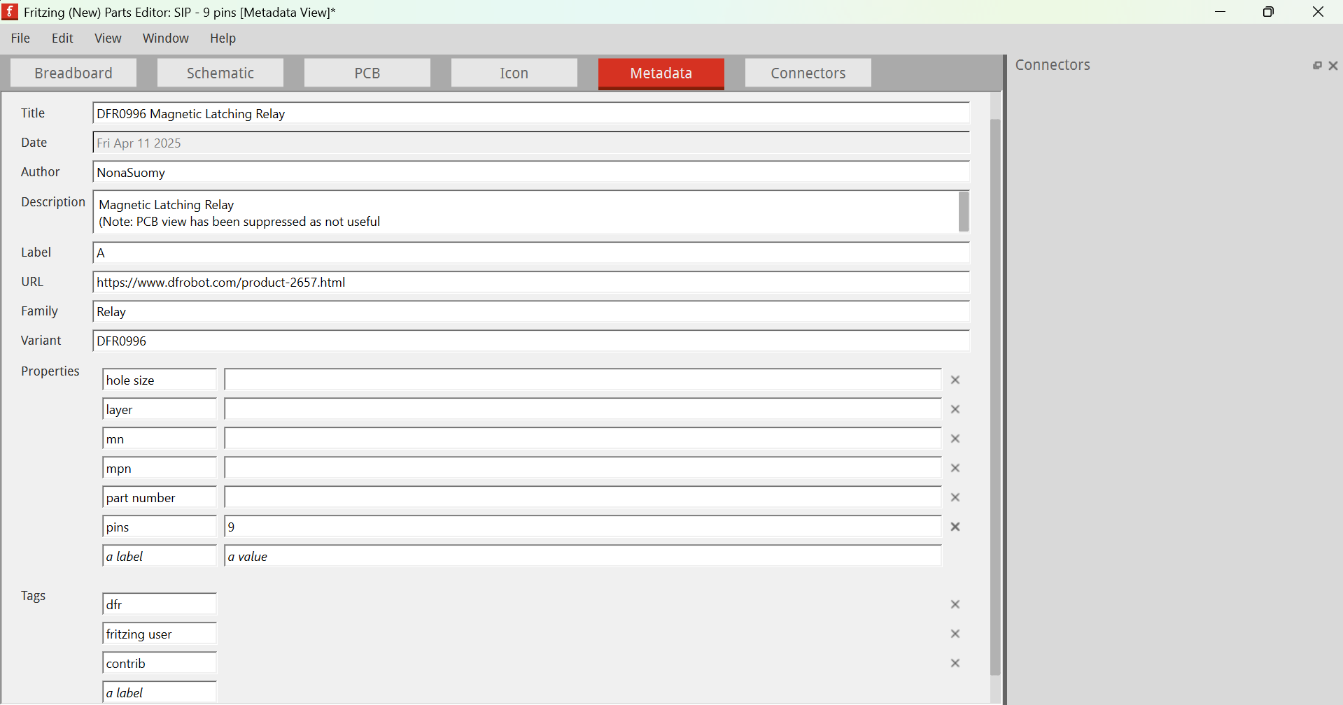
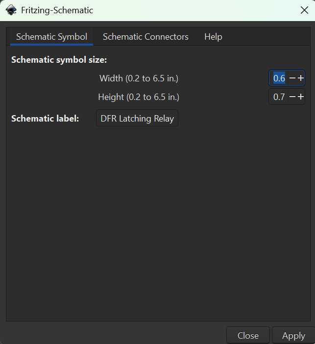
First go to the metadata tab and change to
Next, your schematic view is quite broken.
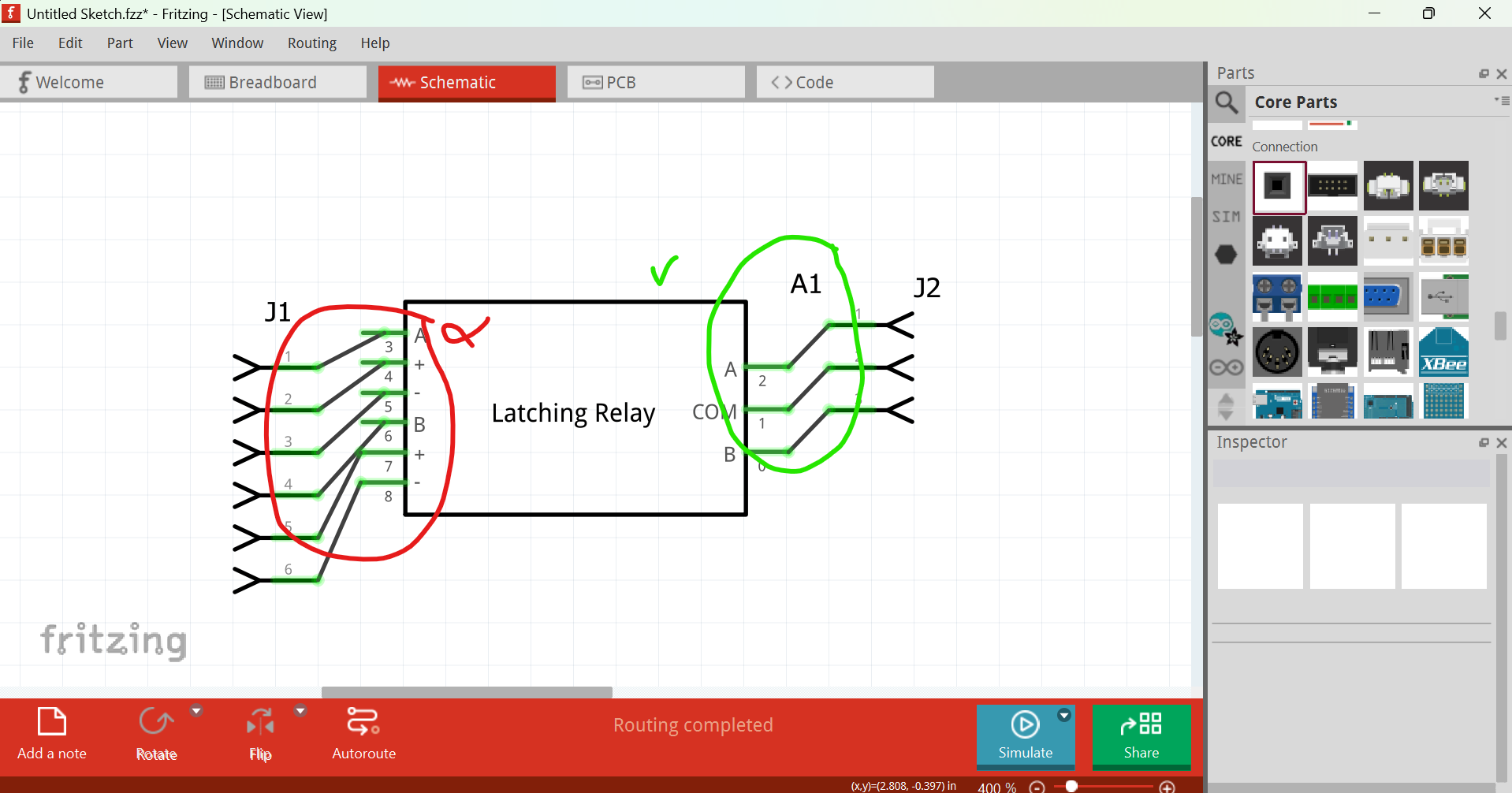
Pins not aligned to 0.1in grid and wire terminates to the centre of the pin!
The easiest way to correct this is to run through Randy’s Inkscape Schematic Extension (documented in @vanepp’s series of part creation tuturials)
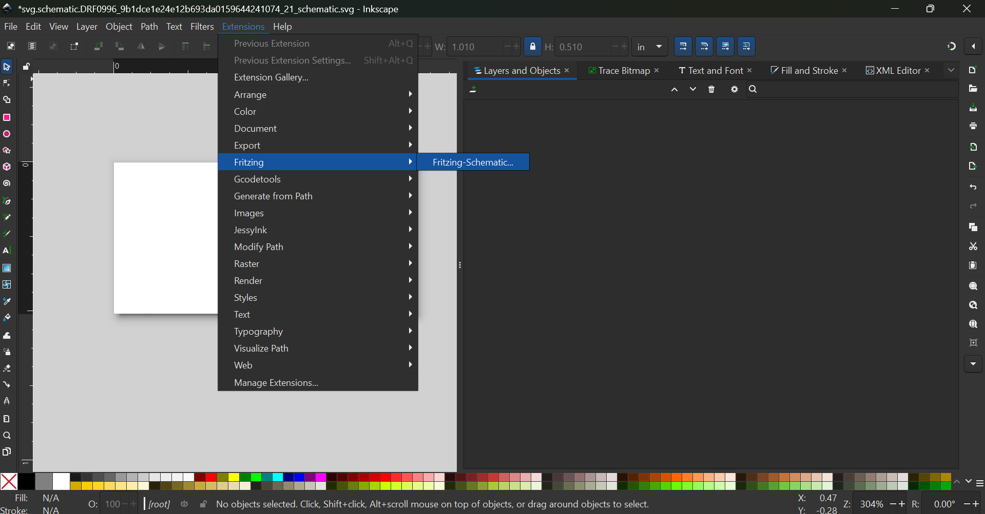
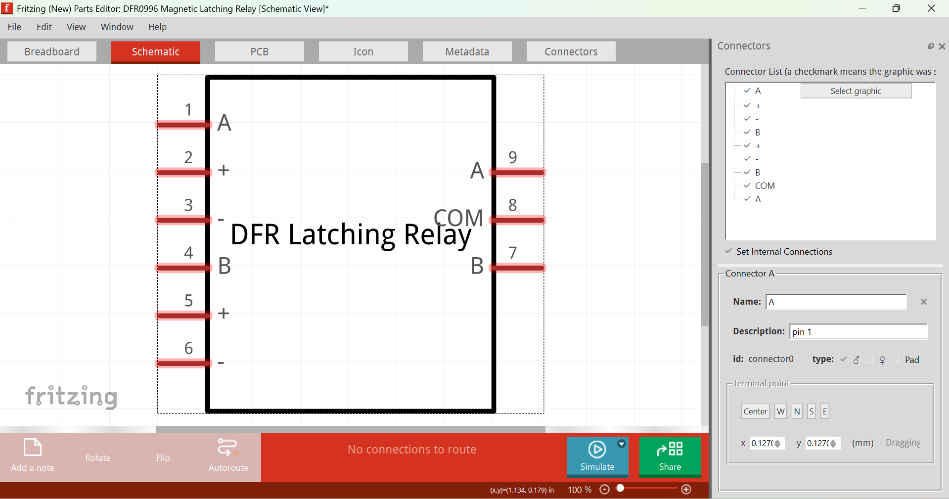
Add the pin labels and you’ll get this SVG here

Load it into Fritzing
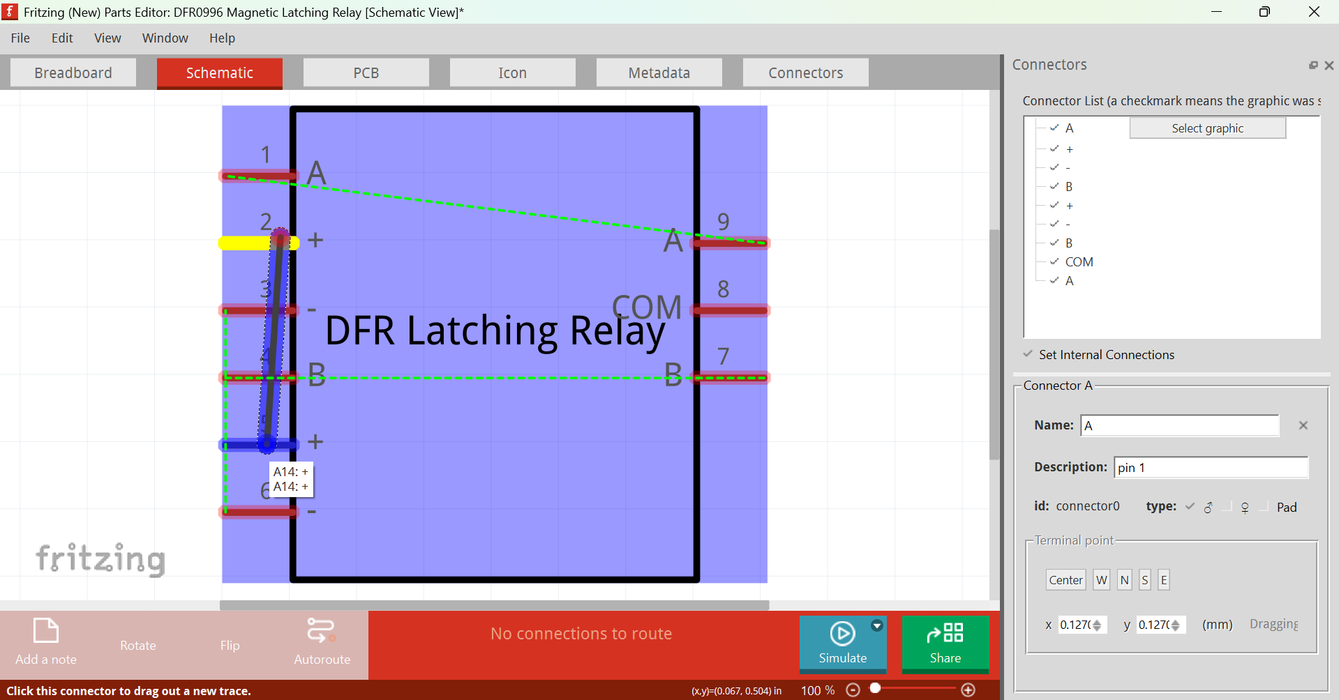
and set internal connections
Save the part
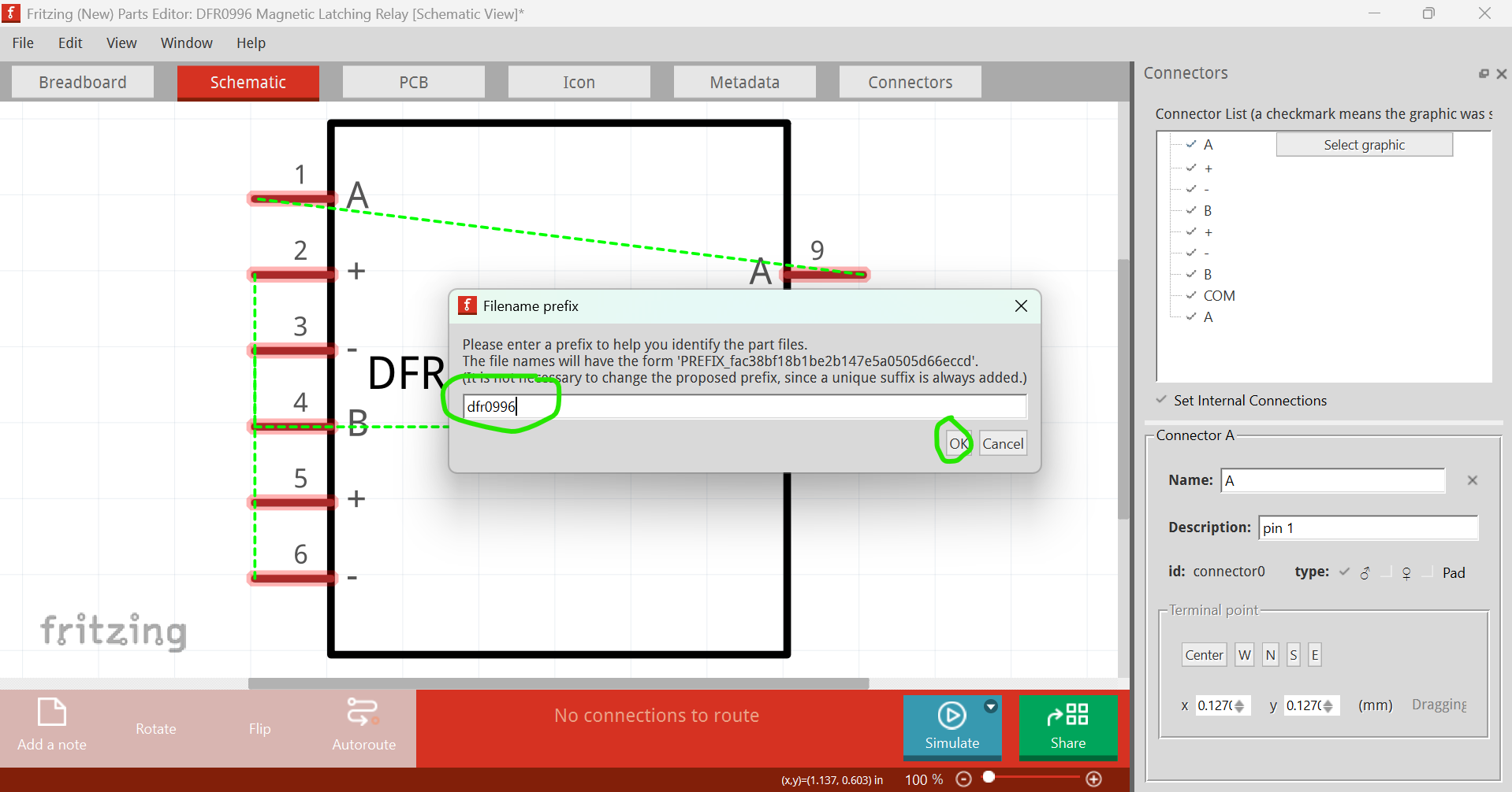
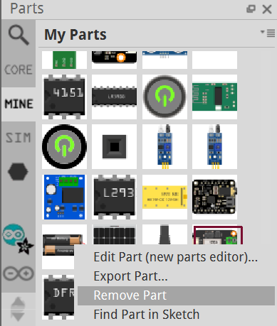
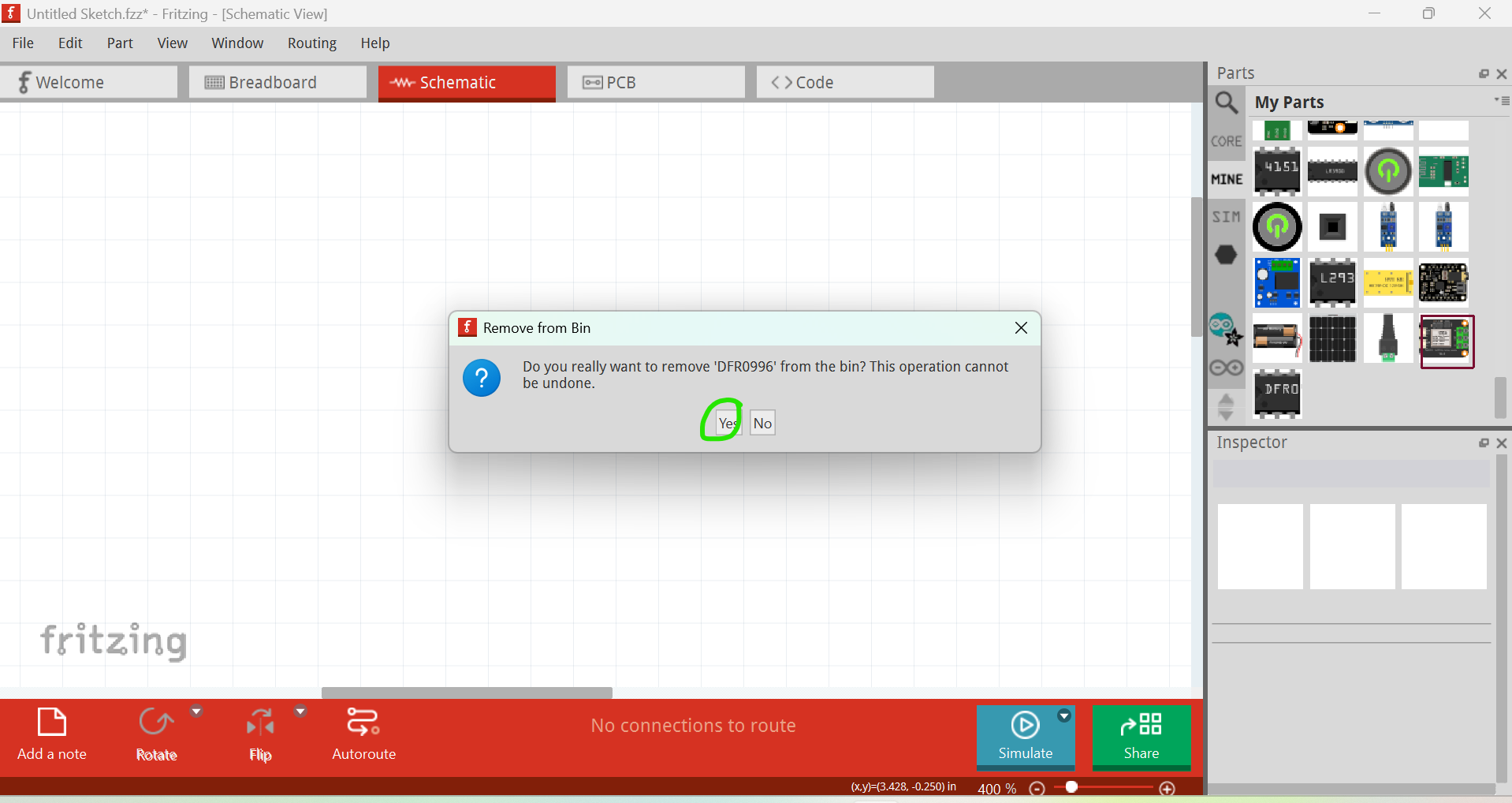
Remove the old one
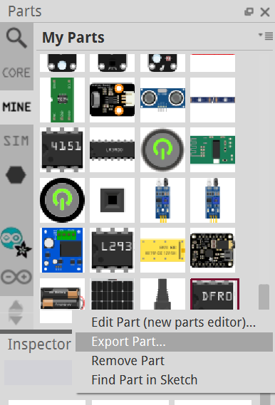
Export the new one
Remove the new one as well, and close fritzing

FZP File
Now that you have the new part, decompress it, and clean up the SVGs (a downside of the new part editor)
Then delete icon and PCB files (they’re not needed)
To suppress PCB view and reuse breadboard image for icon image, change from
 <views>
  <iconView>
   <layers image="icon/dfr0996_fac38bf18b1be2b147e5a0505d66eccd_10_icon.svg">
    <layer layerId="icon"/>
   </layers>
  </iconView>
  <breadboardView>
   <layers image="breadboard/dfr0996_fac38bf18b1be2b147e5a0505d66eccd_10_breadboard.svg">
    <layer layerId="breadboard"/>
   </layers>
  </breadboardView>
  <schematicView>
   <layers image="schematic/dfr0996_fac38bf18b1be2b147e5a0505d66eccd_10_schematic.svg">
    <layer layerId="schematic"/>
   </layers>
  </schematicView>
  <pcbView>
   <layers image="pcb/dfr0996_fac38bf18b1be2b147e5a0505d66eccd_10_pcb.svg">
    <layer layerId="silkscreen"/>
    <layer layerId="copper0"/>
    <layer layerId="copper1"/>
   </layers>
  </pcbView>
 </views>
to
 <views>
  <iconView>
   <layers image="breadboard/dfr0996_fac38bf18b1be2b147e5a0505d66eccd_10_breadboard.svg">
    <layer layerId="breadboard"/>
   </layers>
  </iconView>
  <breadboardView>
   <layers image="breadboard/dfr0996_fac38bf18b1be2b147e5a0505d66eccd_10_breadboard.svg">
    <layer layerId="breadboard"/>
   </layers>
  </breadboardView>
  <schematicView>
   <layers image="schematic/dfr0996_fac38bf18b1be2b147e5a0505d66eccd_10_schematic.svg">
    <layer layerId="schematic"/>
   </layers>
  </schematicView>
  <pcbView>
   <layers image="breadboard/dfr0996_fac38bf18b1be2b147e5a0505d66eccd_10_breadboard.svg">
    <layer layerId="breadboard"/>
   </layers>
  </pcbView>
 </views>
The description needs cleaning up, so change from
<description><!DOCTYPE HTML PUBLIC "-//W3C//DTD HTML 4.0//EN" "http://www.w3.org/TR/REC-html40/strict.dtd">
<html><head><meta name="qrichtext" content="1" /><meta charset="utf-8" /><style type="text/css">
p, li { white-space: pre-wrap; }
hr { height: 1px; border-width: 0; }
li.unchecked::marker { content: "\2610"; }
li.checked::marker { content: "\2612"; }
</style></head><body style=" font-family:'Segoe UI'; font-size:9pt; font-weight:400; font-style:normal;">
<p style=" margin-top:0px; margin-bottom:0px; margin-left:0px; margin-right:0px; -qt-block-indent:0; text-indent:0px;">Magnetic Latching Relay</p>
<p style=" margin-top:0px; margin-bottom:0px; margin-left:0px; margin-right:0px; -qt-block-indent:0; text-indent:0px;">(Note: PCB view has been suppressed as not useful</p></body></html></description>
to
 <description>Magnetic Latching Relay

(Note: PCB view has been suppressed as not useful</description>
and change from
  <connector id="connector0" name="A" type="male">
   <description>pin 1</description>
   <views>
    <breadboardView>
     <p layer="breadboard" svgId="connector0pin" terminalId="connector0terminal"/>
    </breadboardView>
    <schematicView>
     <p layer="schematic" svgId="connector0pin" terminalId="connector0terminal"/>
    </schematicView>
    <pcbView>
     <p layer="copper0" svgId="connector0pin"/>
     <p layer="copper1" svgId="connector0pin"/>
    </pcbView>
   </views>
to
  <connector id="connector0" name="A" type="male">
   <description>pin 1</description>
   <views>
    <breadboardView>
     <p layer="breadboard" svgId="connector0pin" terminalId="connector0terminal"/>
    </breadboardView>
    <schematicView>
     <p layer="schematic" svgId="connector0pin" terminalId="connector0terminal"/>
    </schematicView>
   </views>
  </connector>
Do same for all other connectors.
For connector6, 7 and 8, change from
  <connector id="connector6" name="B" type="male">
   <description>pin 7</description>
   <views>
    <breadboardView>
     <p layer="breadboard" svgId="connector6pin" terminalId="connector6terminal"/>
    </breadboardView>
    <schematicView>
     <p layer="schematic" svgId="connector6pin" terminalId="connector6terminal"/>
    </schematicView>
   </views>
 <connector>
to
  <connector id="connector6" name="B" type="male">
   <description>pin 7</description>
   <views>
    <breadboardView>
     <p layer="breadboard" svgId="connector6pin"/>
    </breadboardView>
    <schematicView>
     <p layer="schematic" svgId="connector6pin" terminalId="connector6terminal"/>
    </schematicView>
   </views>
 </connector>
1 Like
Unusual I used it here and seemed ok, which version of fritzing are you using?
Edit oh you mean on the trace it’s terminating on the center of it. That is because I made the connection point really long so it seems that it attaches to the center of a long trace.
Updated to the end of the board:
DFR0996.fzpz (37.5 KB)
Wait I’m fixing your part
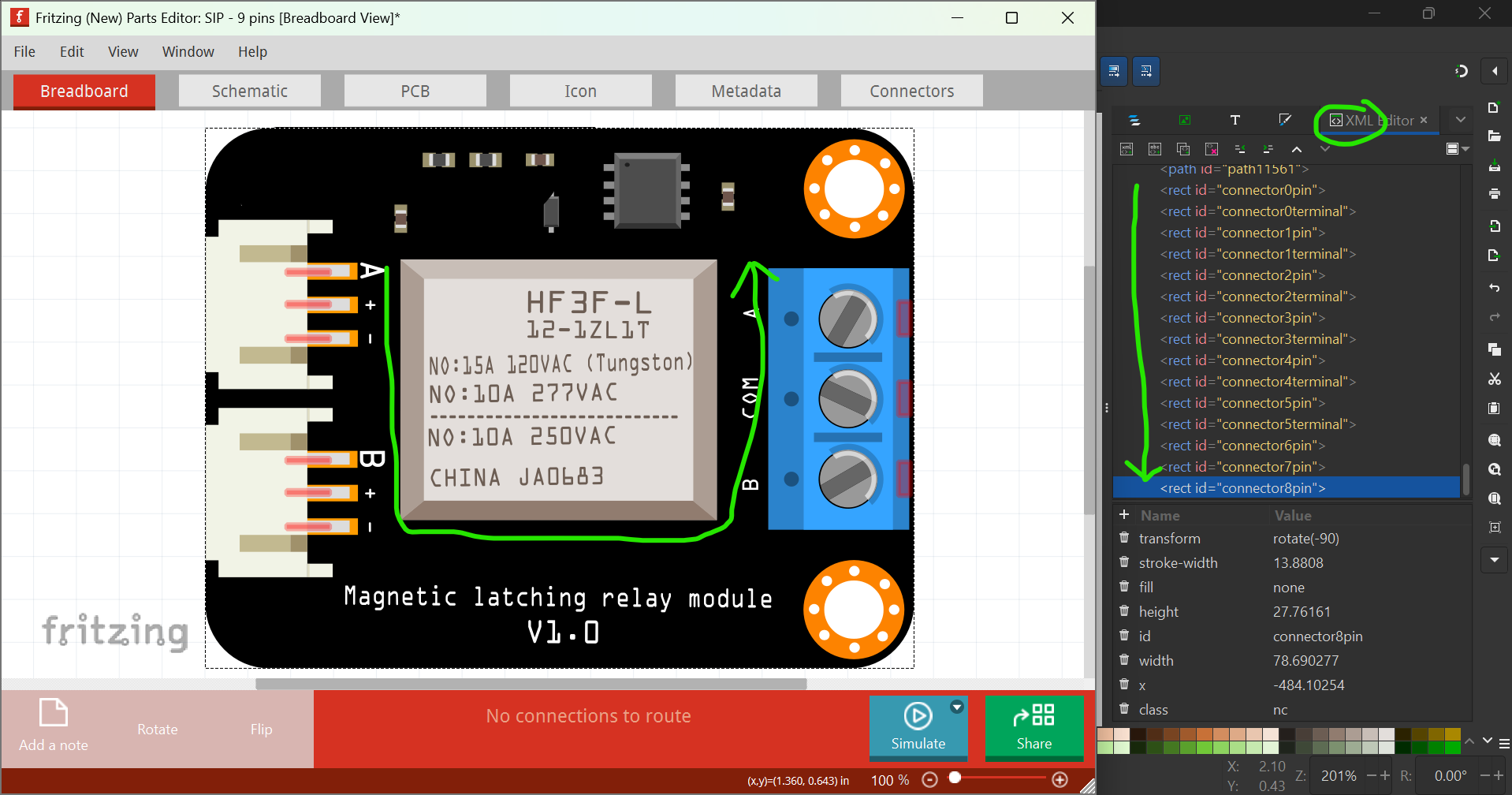
My main issue is I don’t know how to click a connection point when its under another rectangle or invisible colour.
This is because you have to label connectors in SVG like this:
- connector0pin
- connector0terminal
- connector1pin
- connector1terminal
- connector2pin
…
and so on.
Loading the svg into the new part editor should get the correct result.
As I’ve said, I’m fixing your part
Do look at my log of fixing the part
1 Like
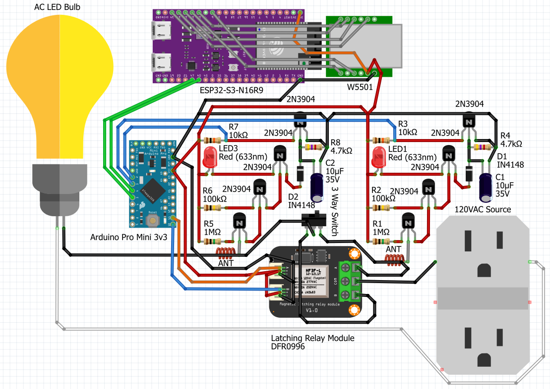
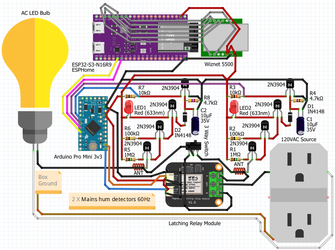
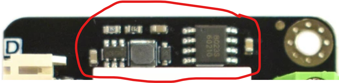
The relay driver circuit at the top seems to have got mangled a bit in your pictures not sure why.
What do you mean by that?

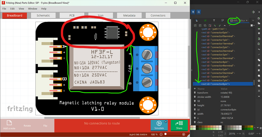
Ah I wondered why when I renamed them in inkscape they didn’t seem to have any effect… inkscape has its own labels…
This is because you renamed them through inkscape, and not XML editor
By the wsy, you don’t have to rename other objects. Leave them as it is. Don’t waste your time
There’s no need to focus too much into the details. It’s fine as long as connectors and main graphics (like the relay) are there
I’m still working on your part
By the way, did you use the extension
Did you use the schematic extension?
1 Like