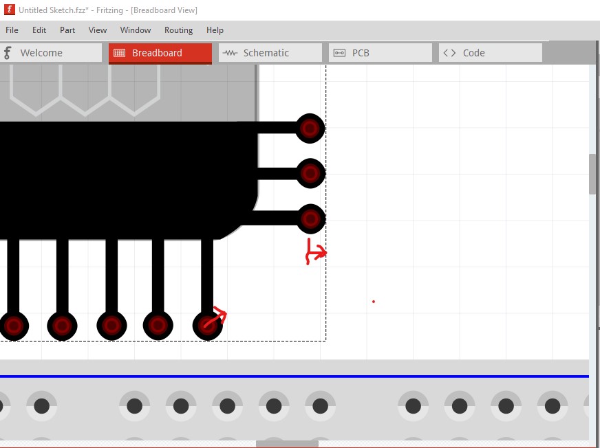
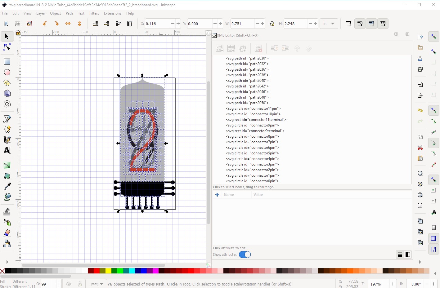
Some difficulties: Breadboard doesn’t align to the grid
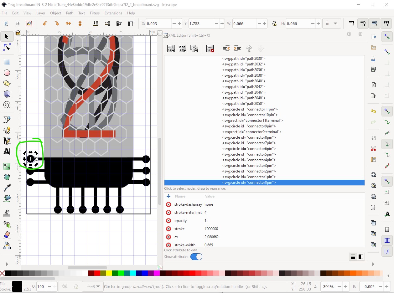
It needs to move a bit in x and y to align. In the breadboard svg if I take connector 0 pin as the base at x 0.003in y 1.753
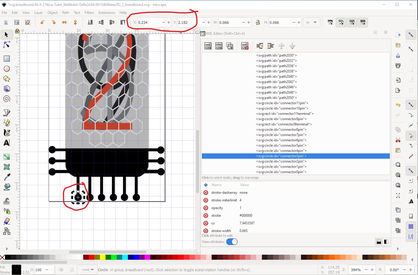
then connector1 pin needs to move a bit in x and y to be .1in apart. In practice I will move connector0pin to be 0 in x and connector1 pin to be 1.853in to set it on the .1in boundary. Connector3pin is more of a problem:
it is 0.234 in x (thus needs to move to 0.2 to be on the grid in x) and 2.182 in y and needs to move to 2.1853 to be on the grid. The 0.034 shift in x means we need to move the entire image 0.034in left to leave the tube looking correct.
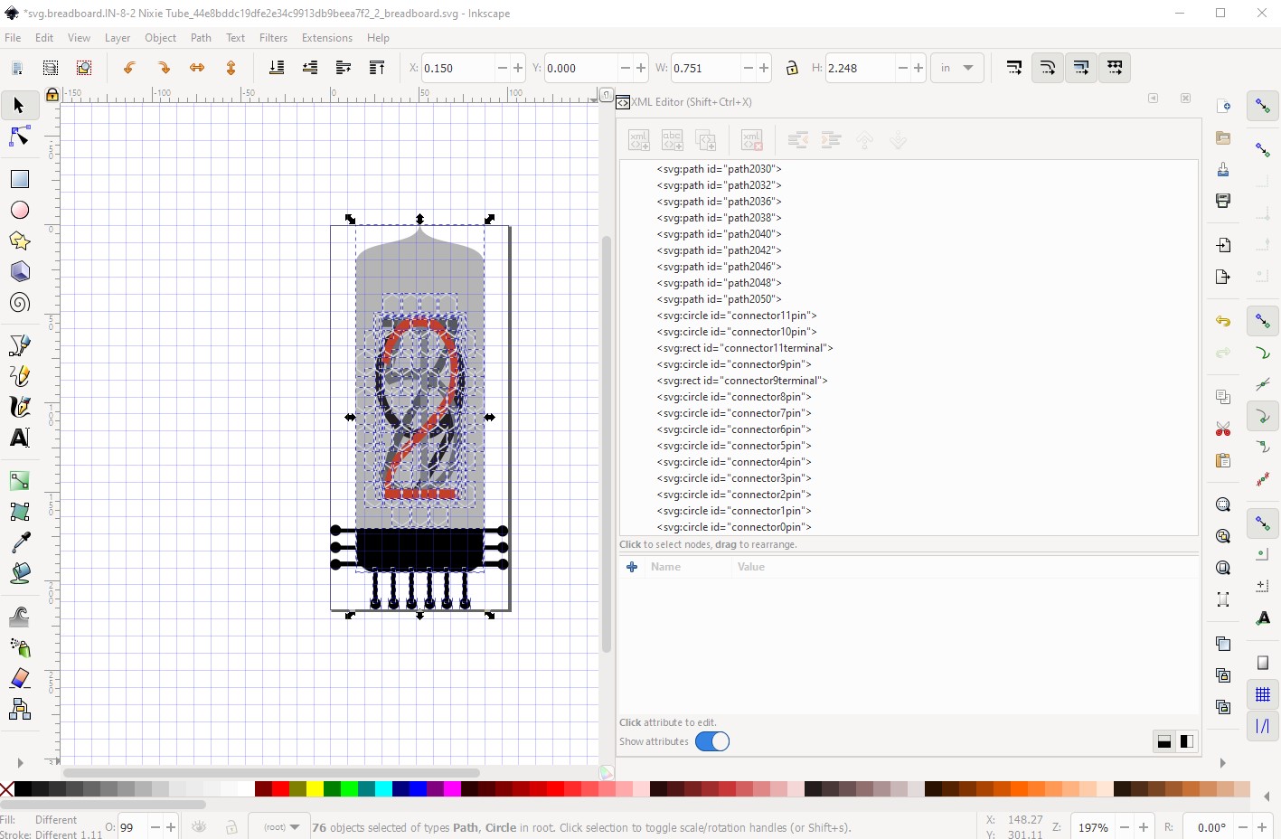
So ungroup (to remove transforms) then select the entire tube and move it from x 0.150in to 0.116 so the connectors are on .1in boundaries.
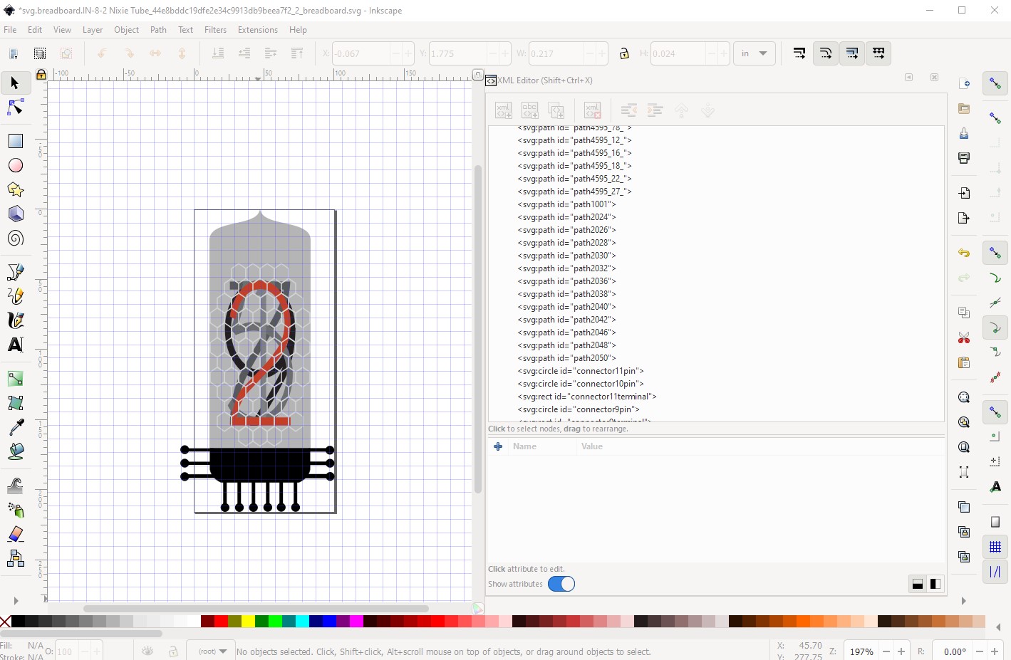
That makes the connector0 row look odd, so move them to make it look better.
Now move connector3pin up in y so that it is on a .1in boundary from the y of connector2pin. Then adjust connector4-8 to be the same in Y and increase exactly .1in in x.
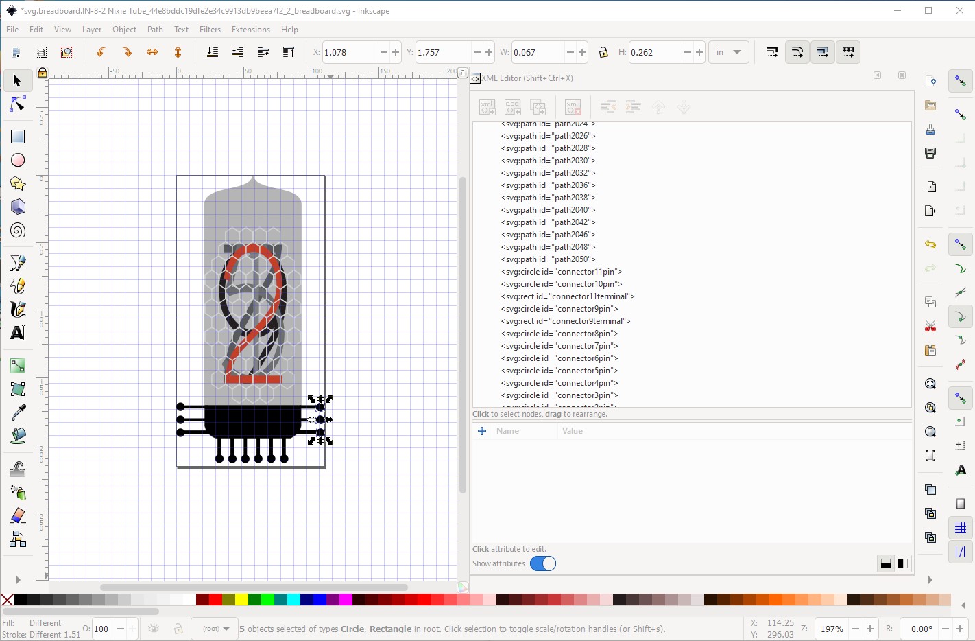
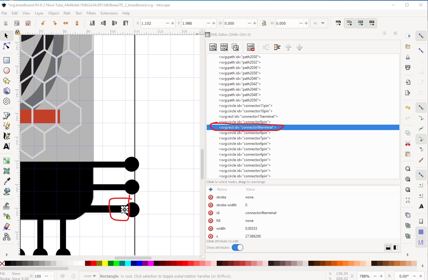
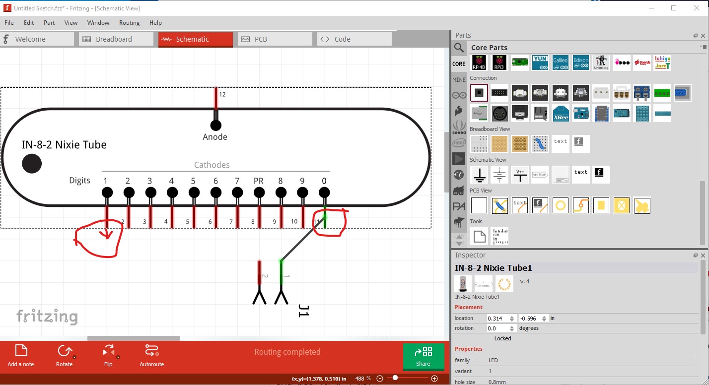
Now we need to align the right side pins to a .1 boundary in x, so they need to change from 1.078in to 1.1in to do that. While I’m here I will delete connector9 and connector11 terminals which are in the wrong place and not needed.
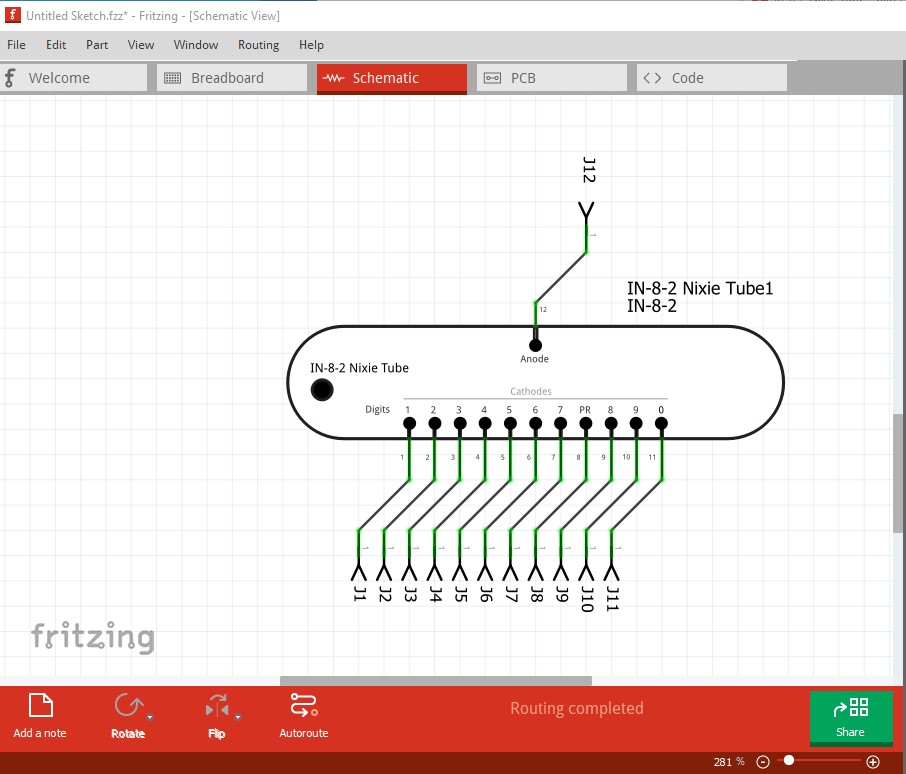
Then I did Edit->select all, Edit->resize page to selection, Object->group, set the group id to breadboard and saved the corrected breadboard svg as plain svg. Now on to schematic. It has some of the same issues, the bottom pins aren’t on the .1 grid in y, in addition it lacks teminalId definitions which causes the wire to connect to the middle of the pin (rather than the end as it should.)
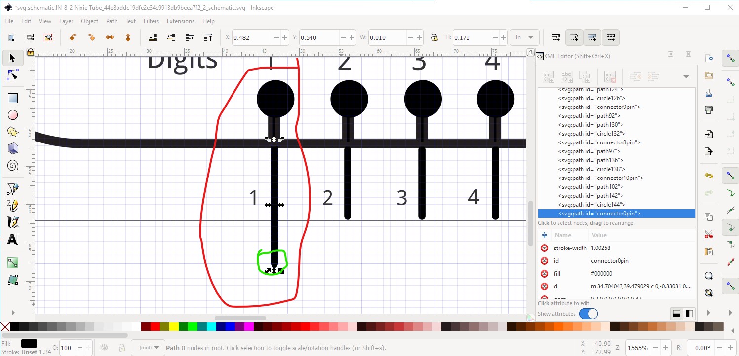
So we will correct both of those by editing the schematic svg. The pins are correctly aligned in x, but the bottom ones are around 0.05in short in Y, so extend connector1pin til its tip is exactly on the .1 grid line
Then set all the rest of the pins to the same height via the tool bar. Now on to the terminalIds. To do that we need to create a rectangle with fill and stroke both set to none and a stroke-width of 0. We then need to set the height and width via the tool bar to 0.01in (to match the width of connector1pin) and use the tool bar (because Inkscape won’t select a no stroke no fill drawing element to drag it) to the correct coords 0.482in x and 0.7in y in this case.
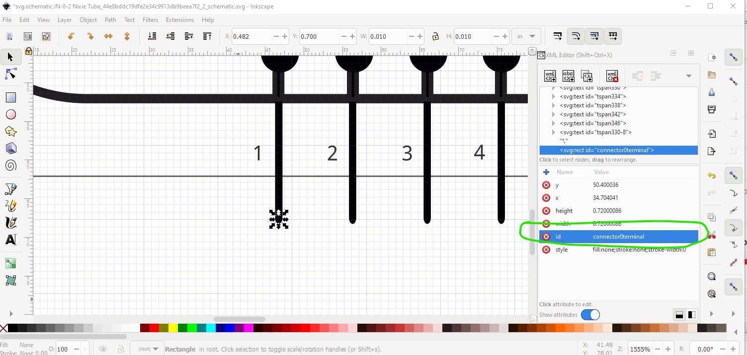
Now we need to set its id to connector0terminal
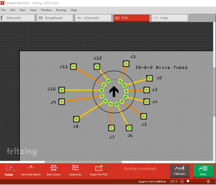
Now duplicate connector0terminal and move it 0.1in across in x and rename it connector1terminal, repeat for all the rest of the pins. The resize, group, change the group id to schematic and save as plain svg and schematic is done. Pcb doesn’t look to need anything. I will note that I prefer to not use paths as connectors. While Fritzing accepts them, changing the hole size later requires editing the path. I prefer to define the pads as circles in which case changing the radius and stroke-width in the xml will change the hole size in a predictable way. All these changes are in this new part which looks like this
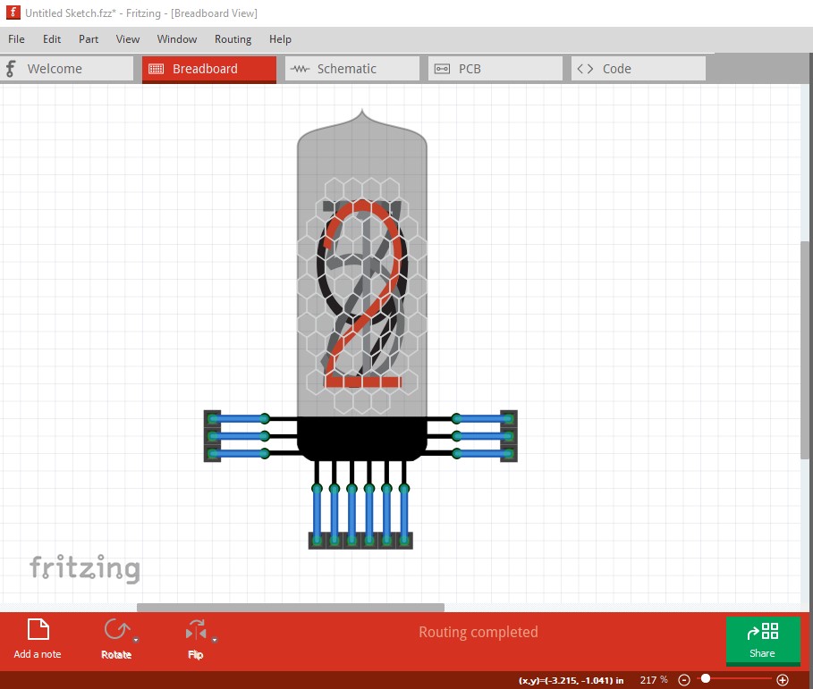
where the pins align on the .1in grid.
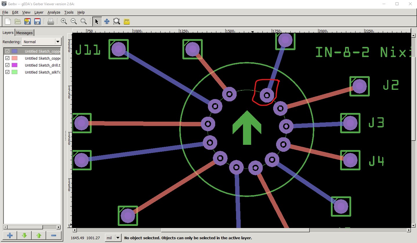
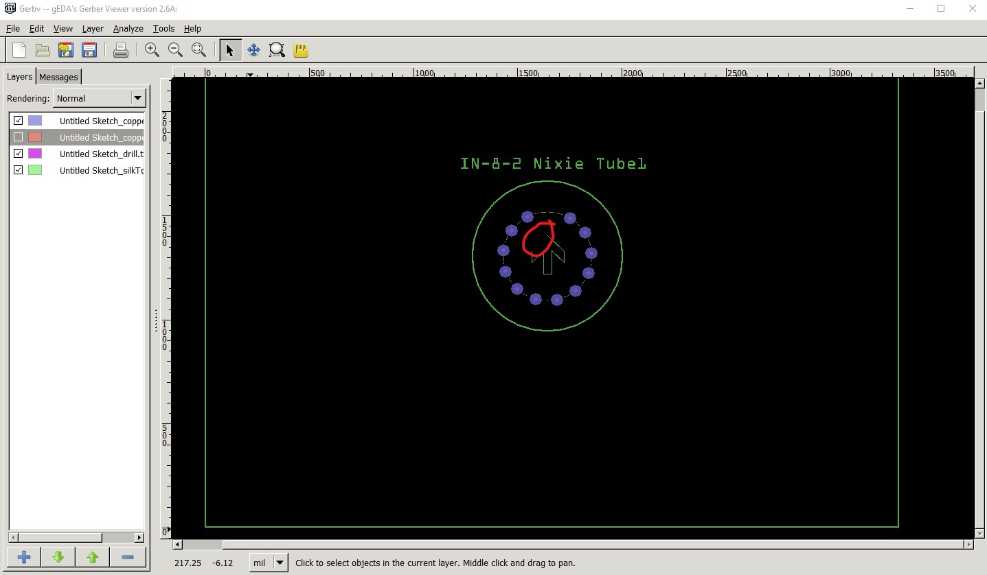
and the wires in schematic connect to the end of the terminal as they should. However a check of the gerber output shows a problem with the path elements as pads:
produces this gerber output (displayed in gerbv)
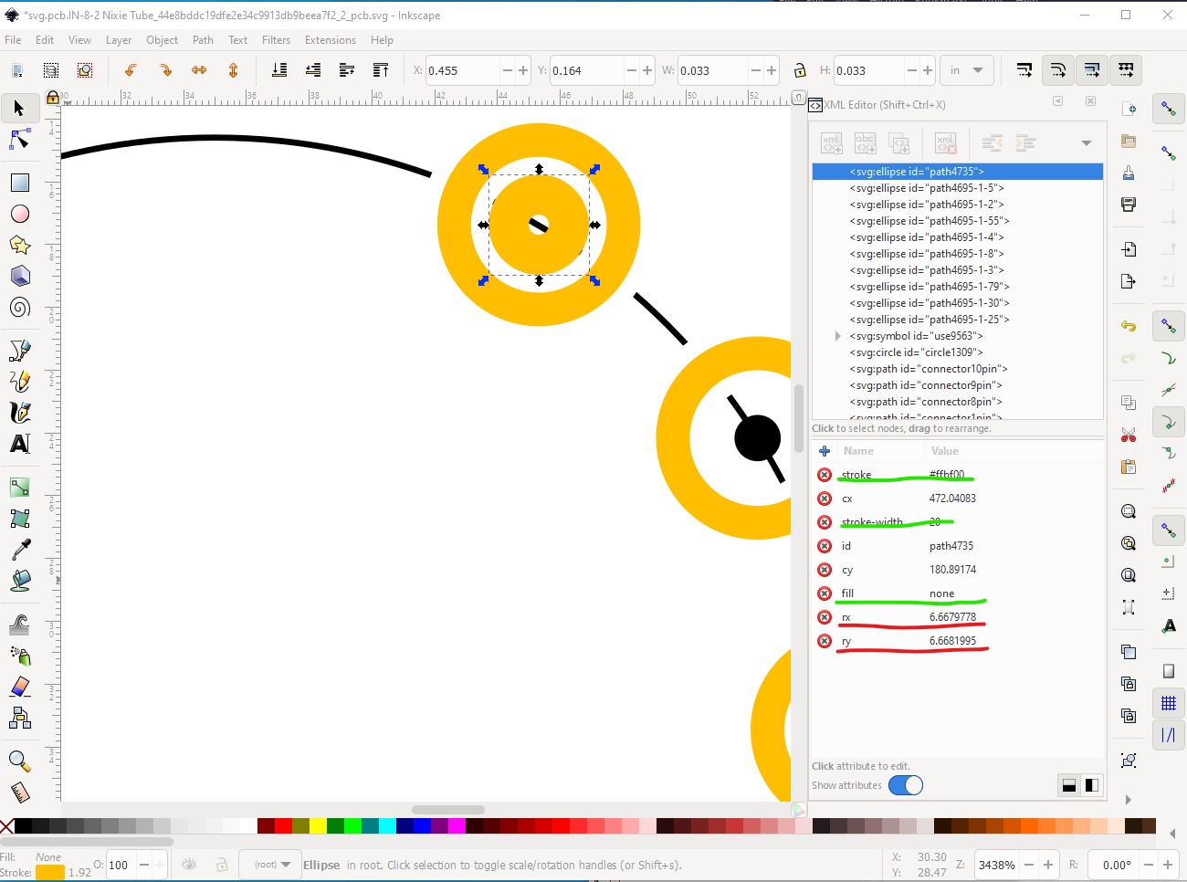
the problem shows in the pad circled in red. The purple dot in the middle of the padis the hole. As we see it does not connect to the ring around the pad which means the hole will not be plated through I don’t think as the pad does not extend to the hole. To fix this I intended to replace the path with a circle, but I discovered that the pad is in two parts, the ring (which is a path) and a separate hole (which is an ellipse, but is being drilled anyway!) The solution is to replace both with a standard connector with a ring like this
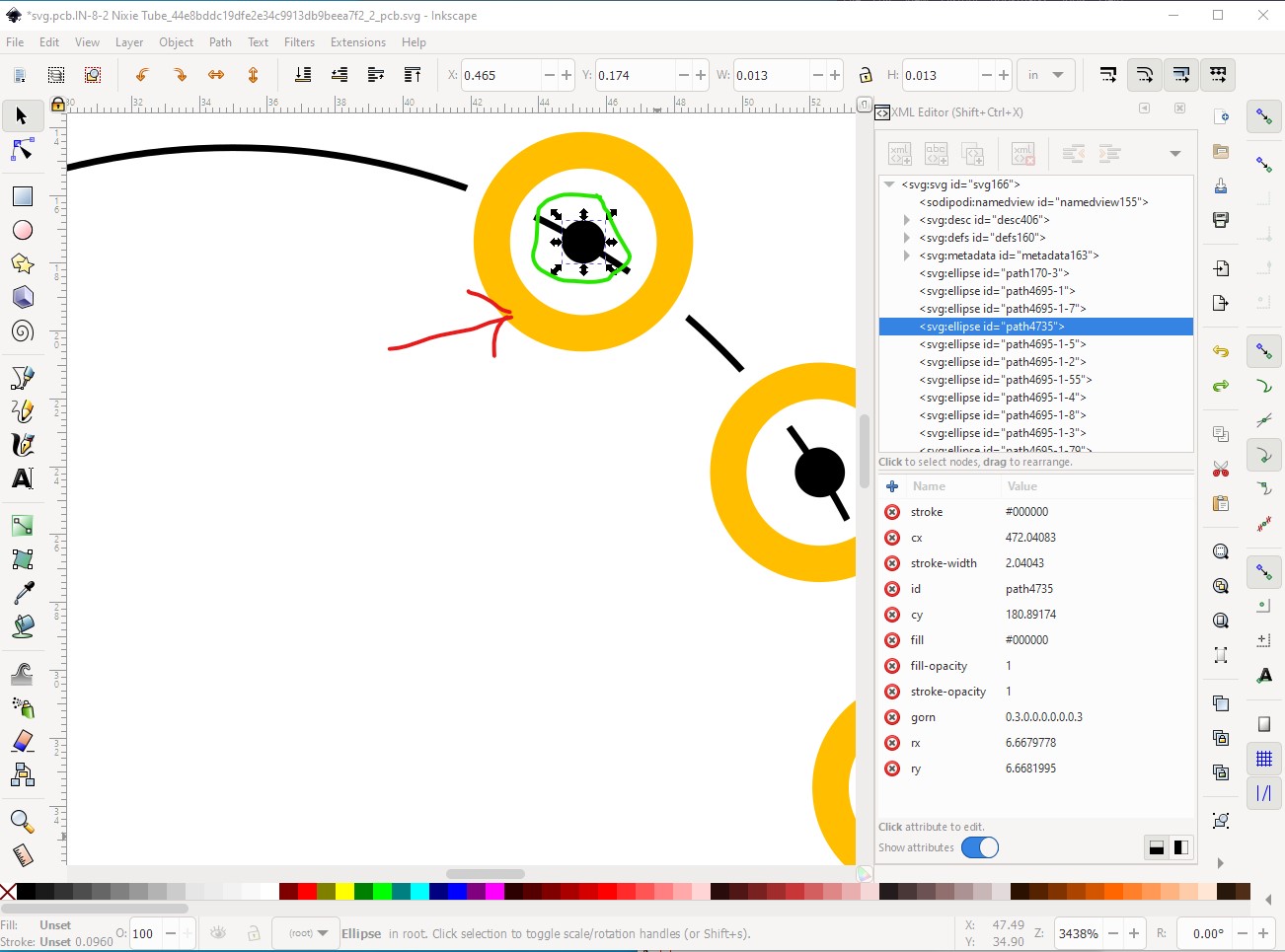
here I am going to replace the ring (red arrow) with a changed circle (green circle). Since the current gerber drill size is 0.017839in round up to 0.018in to make calculations easy (and assuming that is the correct hole size!) In Inkscape the hole size calculation is
hole size = pad diameter + (2 * stroke-width)
in this case I want the diameter of the pad for a 20 thou stroke-width so
pad diameter = hole size + (2 * stroke-width) or
hole size + (2 * stroke-width) = pad diameter
0.018 + ( 2 * 0.02) = 0.058 as the pad diameter. So change the hole to that like this.
here I have changed the stroke color to gold, the fill to none, the stroke width to 20 (which is 0.02in as I also rescaled the drawing to the correct scale to make calculating easier.) As we see the circle is still centered correctly. Now I am going to change rx and ry values to 19 (which is the correct radius for the circle with a pad width of 0.058 in) as changing the radius leaves the circle where is in x and y. Now change the id to connector0pin and delete the orginal path that was connector0pin.
Repeat for all the other pins. Then resize regroup and save as plain svg. That creates this part with correct plated through pads which creates this gerber output with correct plated through hole type pads with a 0.018 dia hole. Something bad has happened to the arrow path on silkscreen though.
and here is the improved part.
IN-8-2 Nixie-improved.fzpz (16.4 KB)
Peter