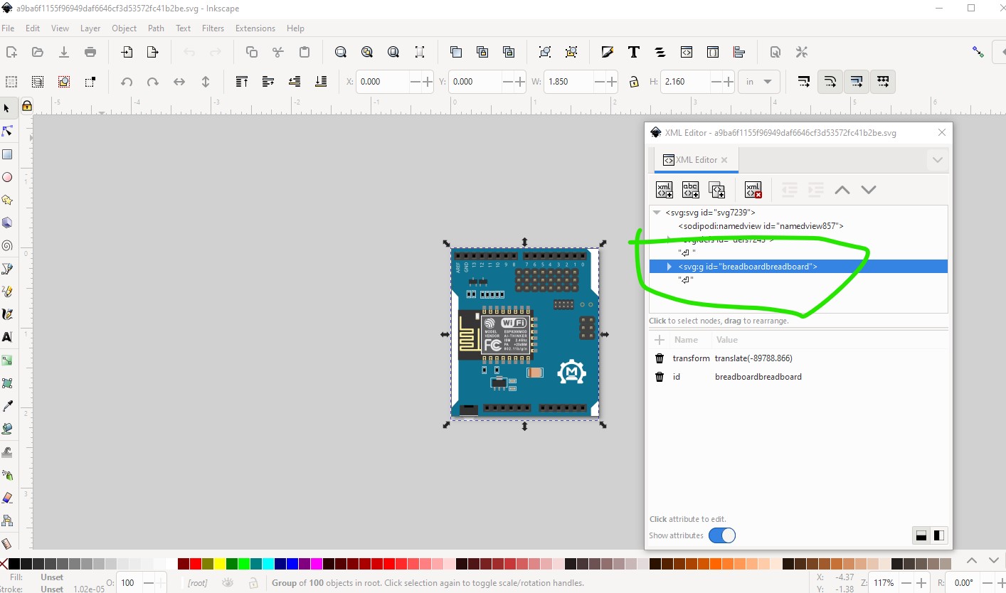
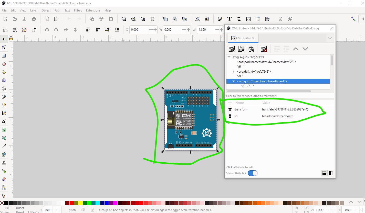
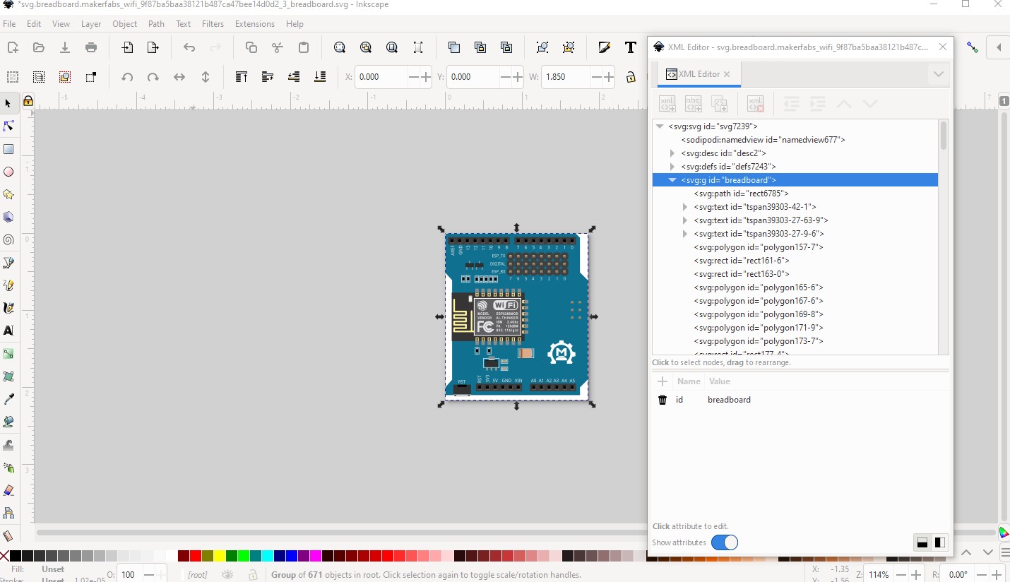
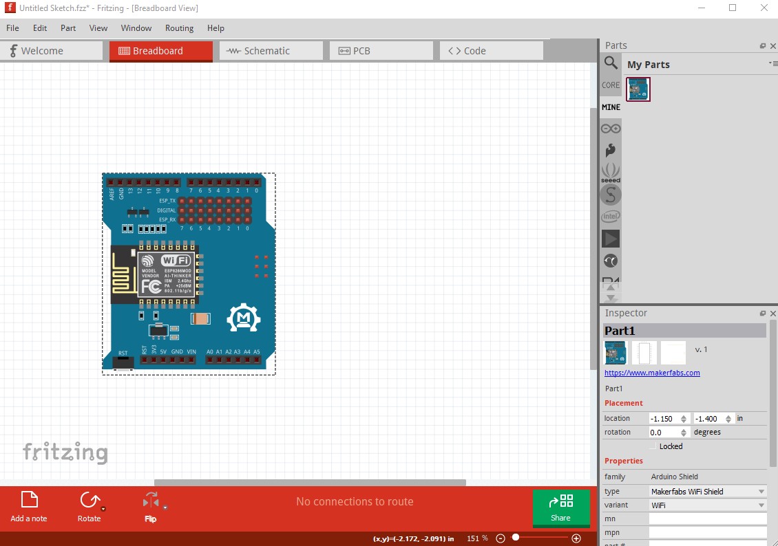
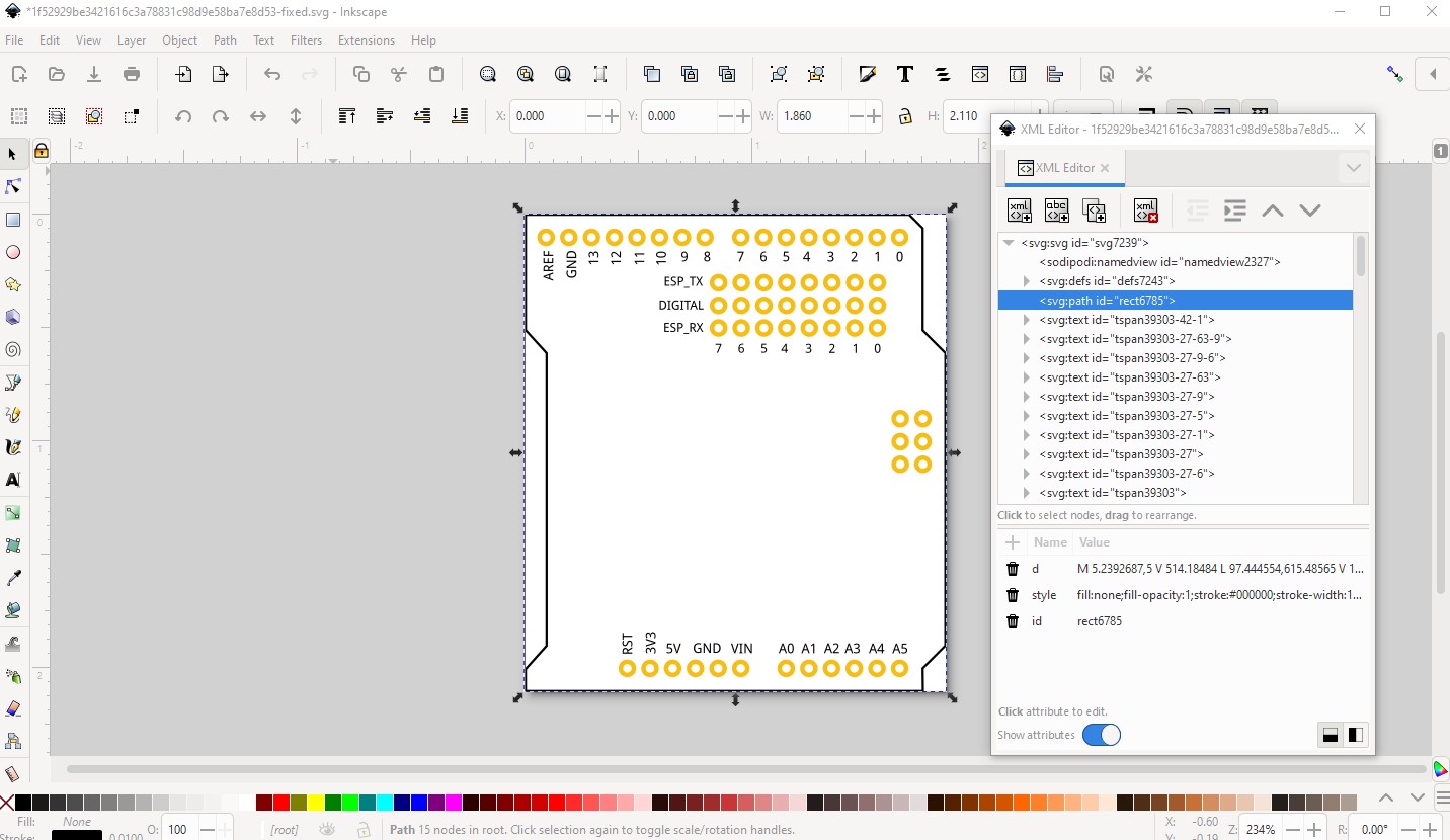
I started with the “zero” microcontroller part as a template for a shield. The zero file was done in Corel apparently. I use Inkscape. I thought it would save me time, but perhaps not How can I clean this up? Somehow there is a group that I can’t find. There is a “breadboardbreadboard” group that Corel created with an id of “breadboard”. I thought of just trying to find the correct ending and just getting rid of it, but not sure if that will break something. I can’t group everything on the board and call it breadboard since that ID already exists. Clicking on it in the XML editor doesn’t highlight anything for me to find it and ungroup it.
I noticed in Inkscape, I have a bunch of return symbols in the XML editor. I’ve not seen that before. It is like it can’t read the XML. Yet the original part worked fine, I just picked a board that had similar connectors and parts for the redesign. I think I am very close if I can get rid of what the file doesn’t need. Then I just have to add the remaining silkscreen labels and assign the connectors.
I must be doing something wrong because nothing ungroups. I can click on the board, which is a different object, or I can use the XML editor to seled “beadboardbreaboard”, but I can hit control-shift-g 100 times and nothing seems to happen
Huh! On Inkscape 1.2.1 (9c6d41e410, 2022-07-14) (and in all the older versions in the past) either selecting the group and doing cntrl-shift-g, or Object->Ungroup ungroups it (and removes all the transforms which is one reason to do it.) You can also change the group Id in xml editor, but ungrouping it to remove the transforms is the preferred method. Don’t know why that doesn’t work for you unless you have removed the keyboard short cuts in which case Object->Un group should still work. You could also try Edit->Select all and try the ungroup, but that should be the same as selecting the group in xml editor.
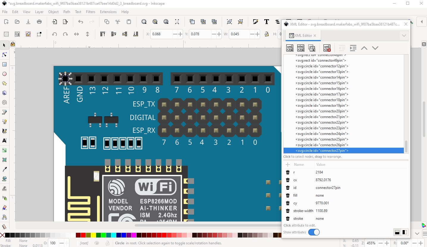
So it works for you? I tried everything I can think of. When I right-click on an object that can’t be ungrouped, “ungroup” isn’t on the menu. I can “select all” and ungroup and everything looks ungrouped, but the “breadboardbreadboard” doesn’t go away using the exact same version of Inkscape as you. When I click on the group, nothing highlights. Does it for you? Like this. Ignore thee dashed lines around the board. I selected it by clicking. Clicking on the group in the xml editor selects nothin in the image:
Why is the group named breadboardbreadboard instead of just breadboard? I see a few boards in Fritzing when I look at them that were created in CorelDraw and have breadboard repeated.
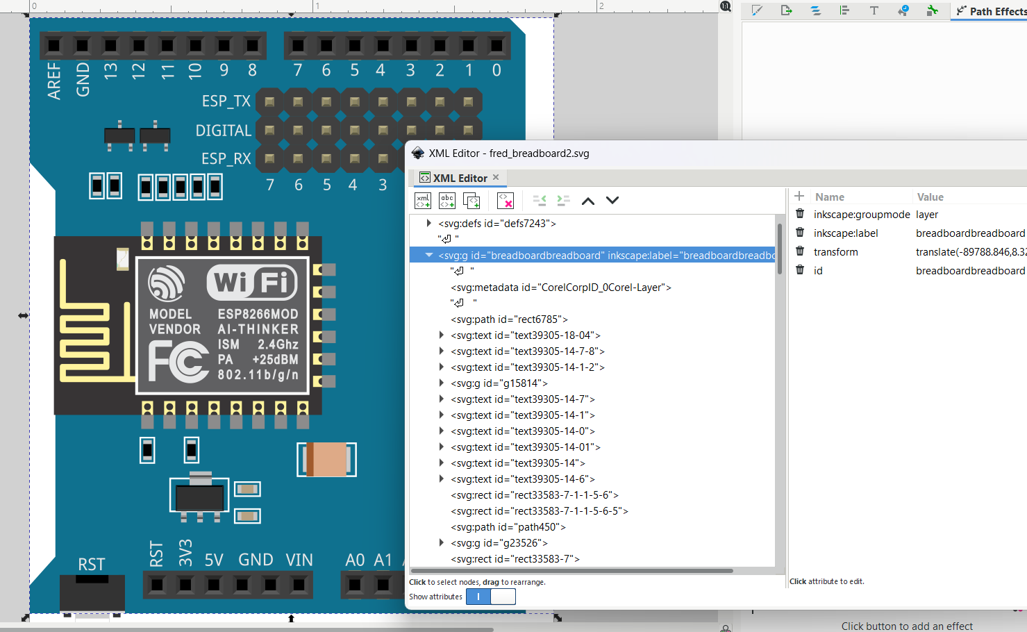
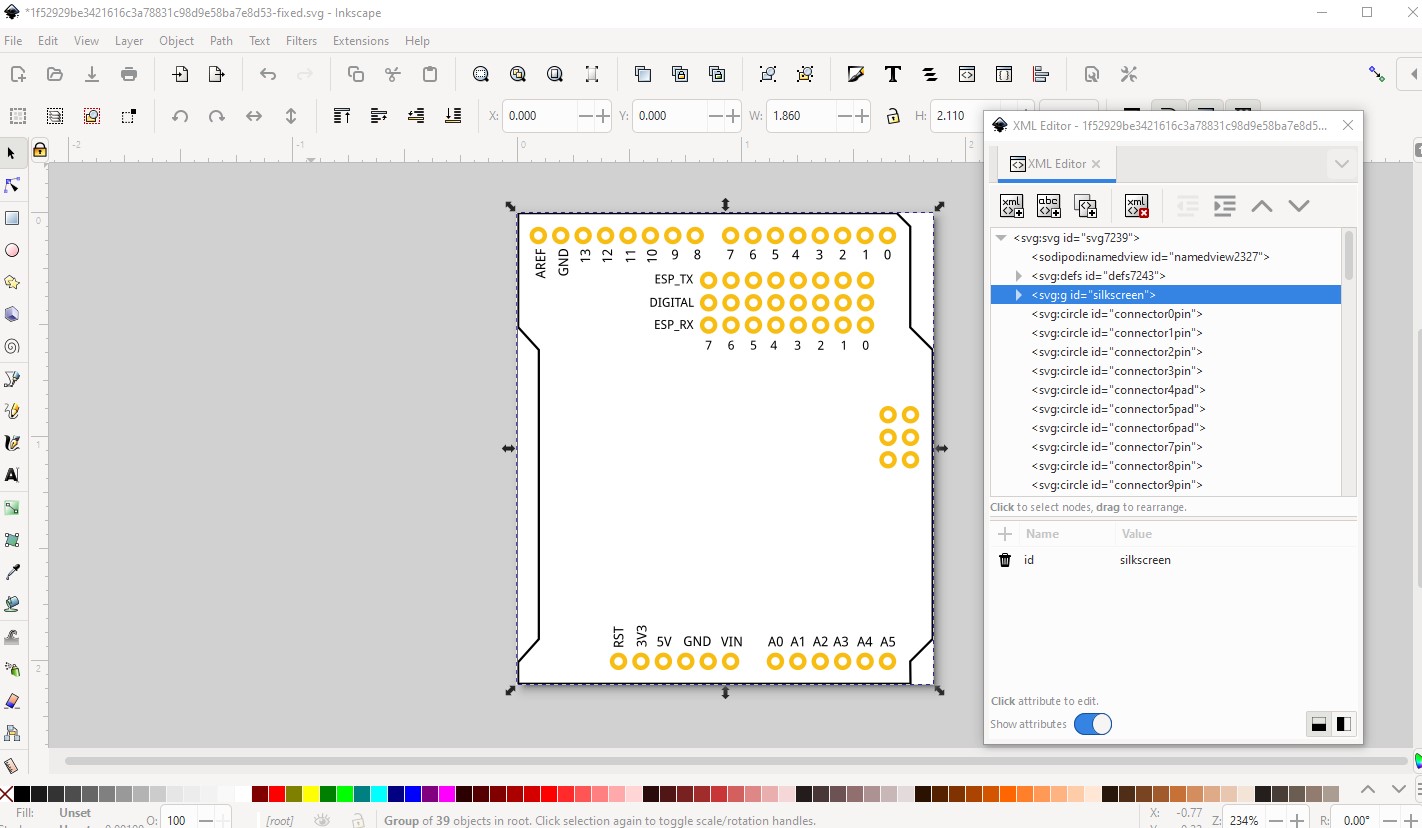
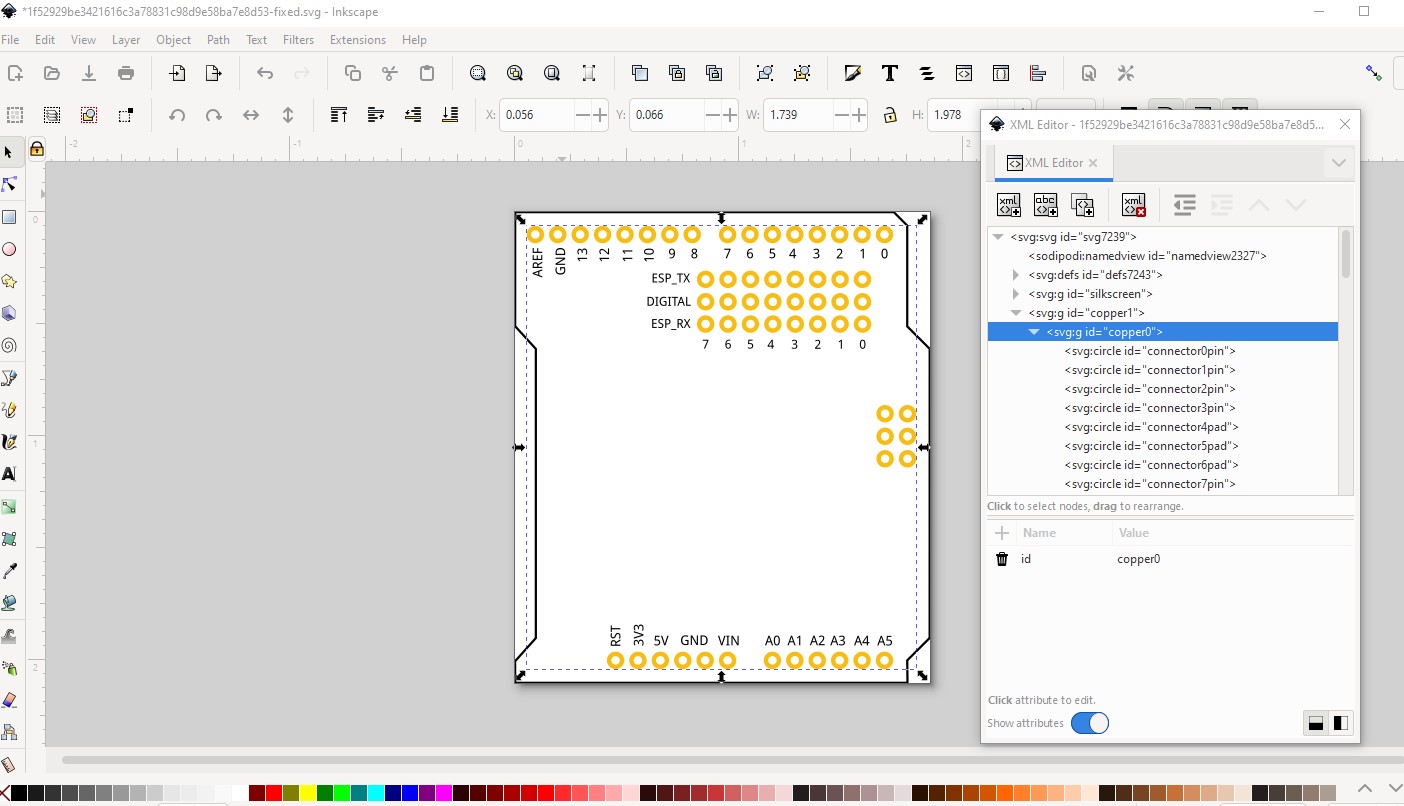
Here is the close to finished version if I can get rid of or rename the breadboardbreadboard group, and rename all the connector pins. You recommend moving the connectors to the bottom of the file, I guess to make it easy to see them all. How do you do that? Removing the line “space=preserve” in a text editor got rid of the carriage return characters.
I think I have all my header and pin spacings correct, but not sure because of the weird way Arduino screws up the spacing between headers and where the ICSP pins are supposed to go. I found a diagram online and worked from that. Here is the file:
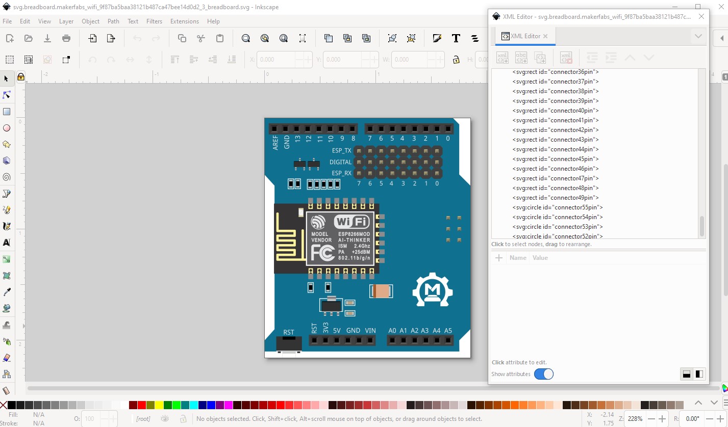
The pin numbering (connector0pin) starts at A0. I saw this on other Arduino boards. I don’t know if that is a standard or just on parts created by “Althaus” or what. It seems to jump around the headers randomly. All the pins in a header are together, but it starts on the analog header, jumps to the top left header, then top right, then lower left. My 3x8 male header connectors are under the group for that header. And the pins are separated by more xml and have connectors associated with them. Not sure how to clean that up to have all the connectors together and how to number them
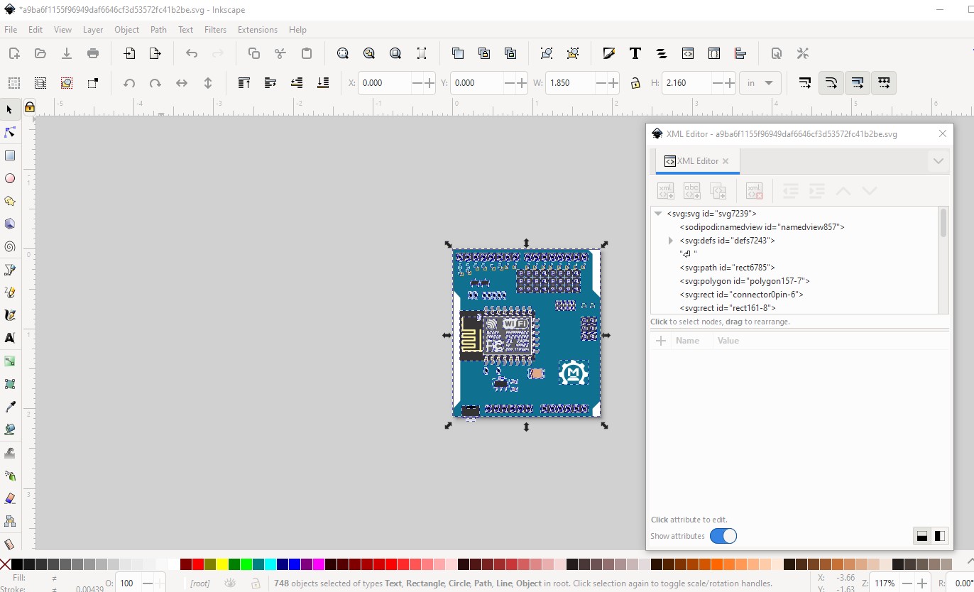
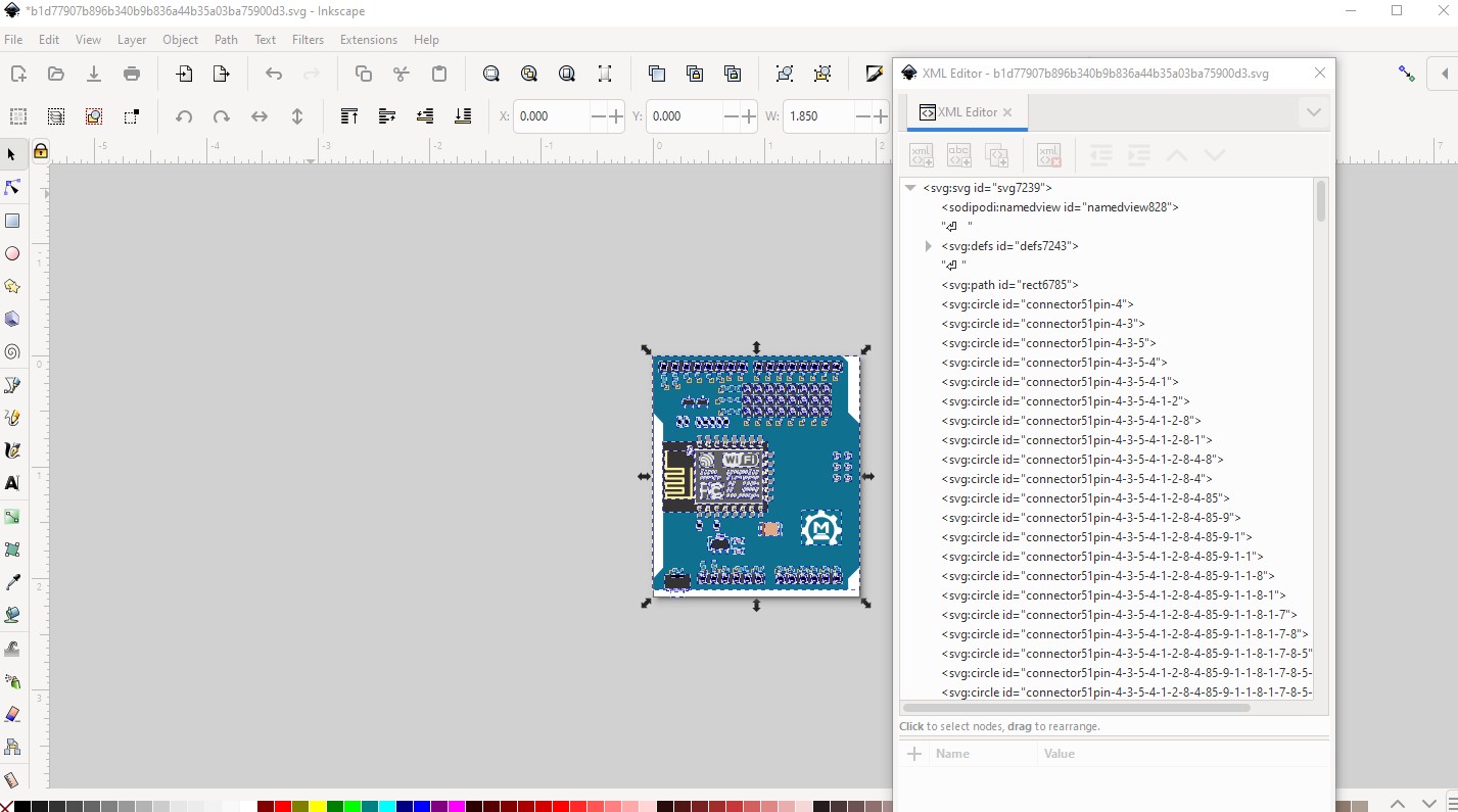
Yep, for me as in the two images in my reply, clicking on the breadboardbreadboard group and ungrouping ungroups the svg as in the second image (and always has for me.)
That too is odd, for me it selects and displays the transform and group id from this
This is inkscape 1.1.2 on Windows10, but as noted this is how Inkscape has always worked for me (from back at 0.9.1.) I would probably be tempted to uninstall and reinstall Inkscape to see if there was a installation error (as unlikely as that seems!) It also may be a setting in preferences although I have no idea what!
breadboardbreadboard (along with the family name) is a special code to indicate this is a breadboard (which you usually don’t want!) The purpose in this case (with only the breadboardbreadboard group name without the rest of the properties required to make a breadboard) is to allow the part to be moved under the breadboard (which for a normal part isn’t possible.) It is mostly done in the arduinos presumably to allow them to be under a breadboard (although I’m not sure why .)
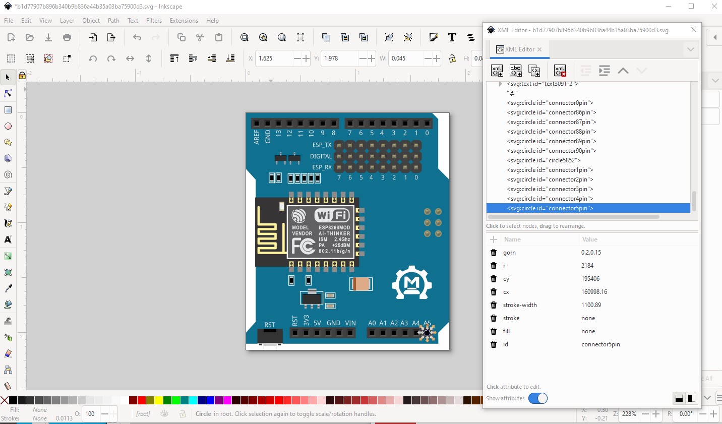
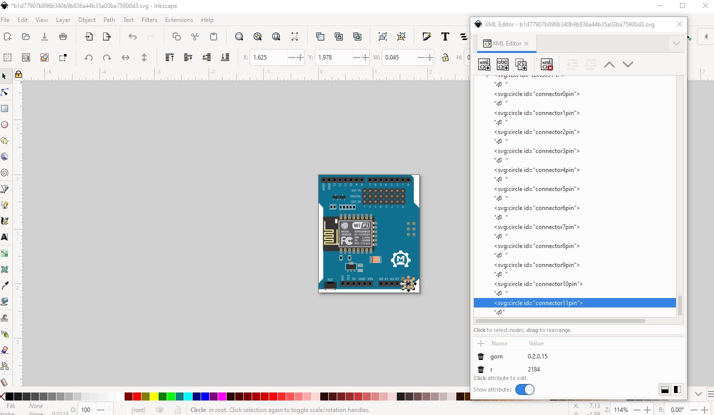
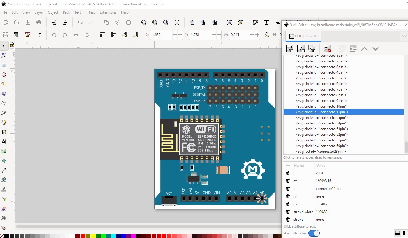
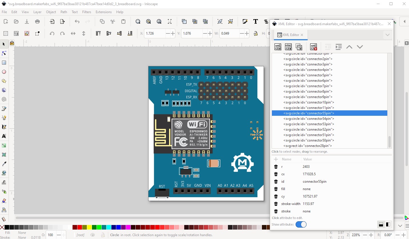
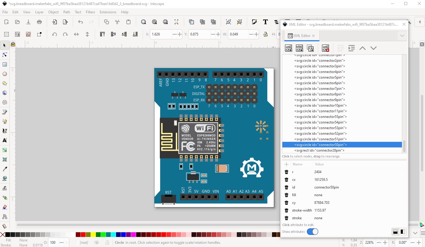
I do this because I have a script that will renumber the pins starting at 0 if they are at the bottom of the svg. To move them select the pins (in order starting where you want connector0pin) and move them to the bottom like this
then click the bottom button on the tool bar to move it to the bottom (note Inkscape 1.2.1 reversed the order of these buttons which is very annoying!) like this:
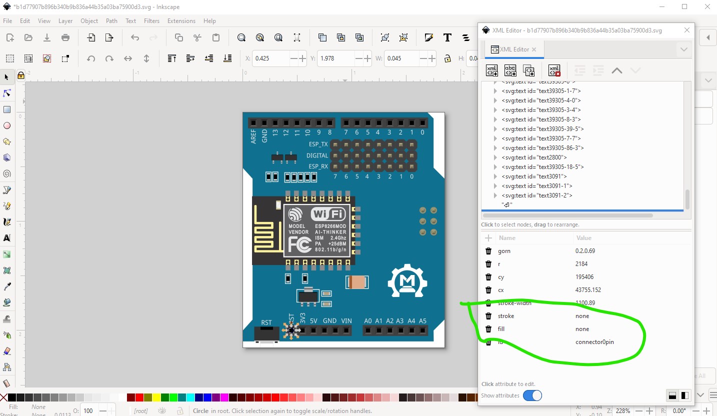
At this point I would set the id to connector0pin which is what the script searches for to start renumbering. Note the circle that defines the connector is now visible so you need to set stroke and fill to none to make it invisible.
(note that the script screws up because there are duplicate pins in the svg and it can’t yet handle that!)
The best bet here is to use the arduino uno part as the base. Here I copy/pasted the uno breadboard in to your svg and then set lines on the edge of the connectors which shows you are a little off. The easy way to fix this is to use the tool bar in x and y. Collect the starting point in x and y for the connectors on the uno and then adjust the ones on your svg to match. An alternative is to start from the UNO svg and just delete what you don’t need (leaving only the connectors.) There is a uno version with the ICSP connectors in core parts.
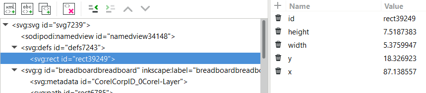
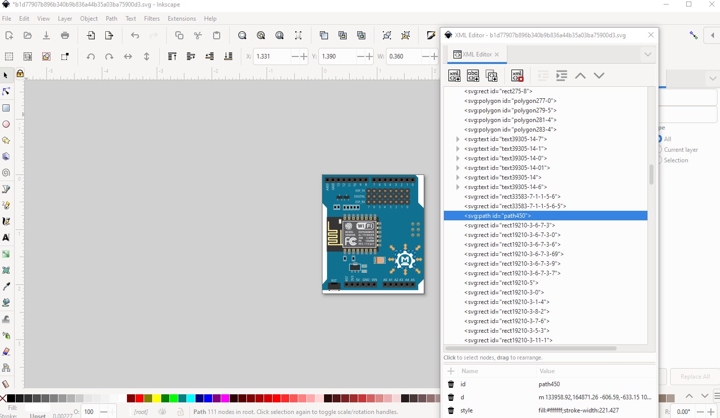
It has no stroke or fill and thus can be deleted as unused, so just select it in xml editor and hit the delete key (then check to make sure there were no unexpected changes in the svg!)
They aren’t random exactly. The Unos (and many other parts) were made from Eagle2Fritzing which converts Eagle brd files to Fritzing. One of its characteristics is odd pin numbering which should be (but often wasn’t) corrected before releasing the part. I have a script which will mostly deal with this as I often use Eagle2Fritzing but again it has too many sharp edges to release yet. My long term goal is to correct all the parts in core to meet the graphics standards which will correct these problems but that is a huge amount of work that hasn’t even started yet except for a handful of parts that needed to be corrected because they are broken (and most of those haven’t made it in to core parts yet.) As I started to do in the example above start at connector 0 on the bottom left of the board and go up in sequence from there (if you are using the schematic extension to make schematic which you should be, note the constraints in the howto I just published on using it!)
I think I’m getting it. Almost finished. I had read the the top headers were .15 apart, but looks like they are .16, so I fixed that.
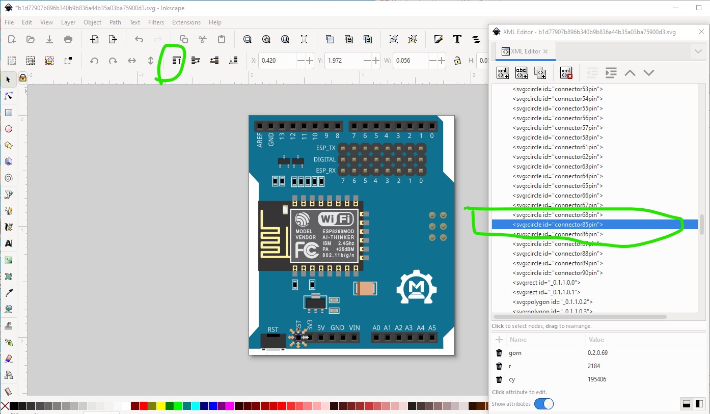
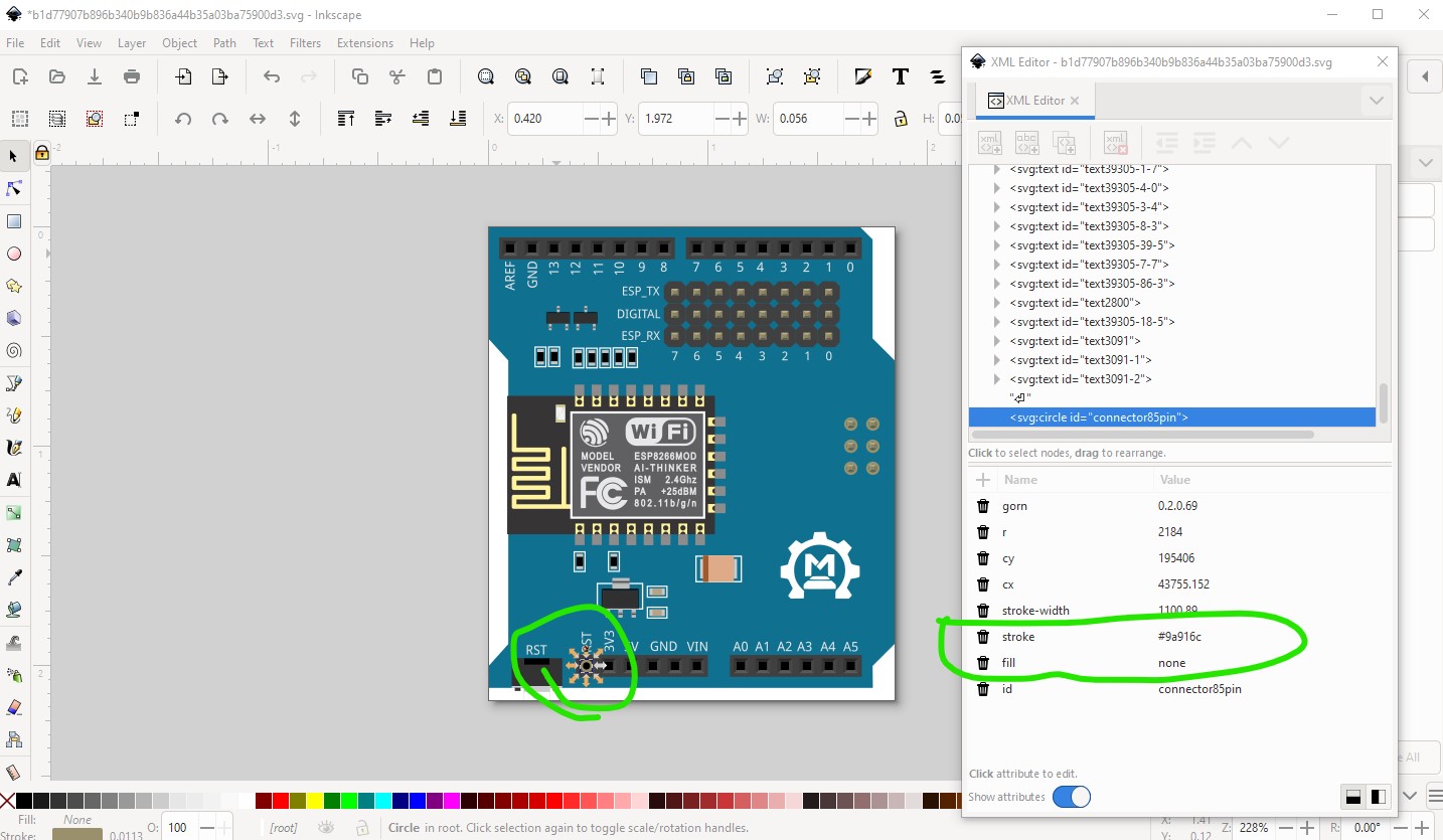
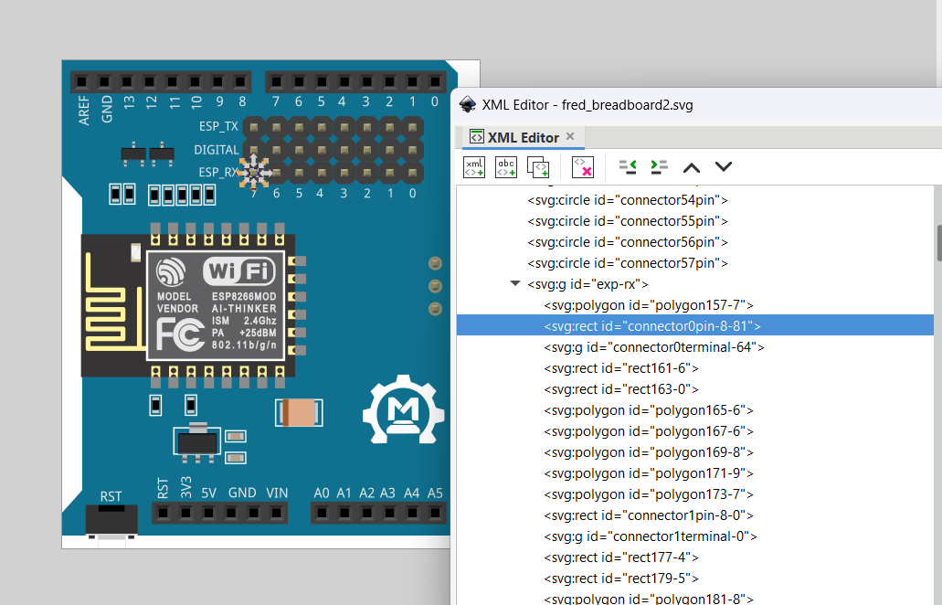
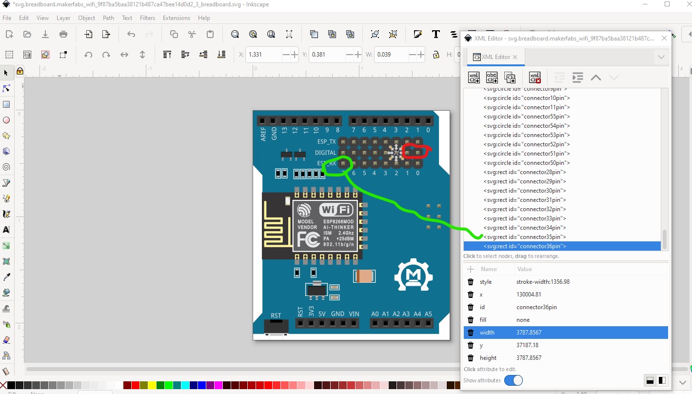
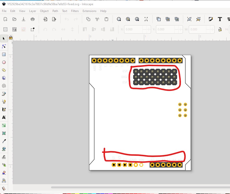
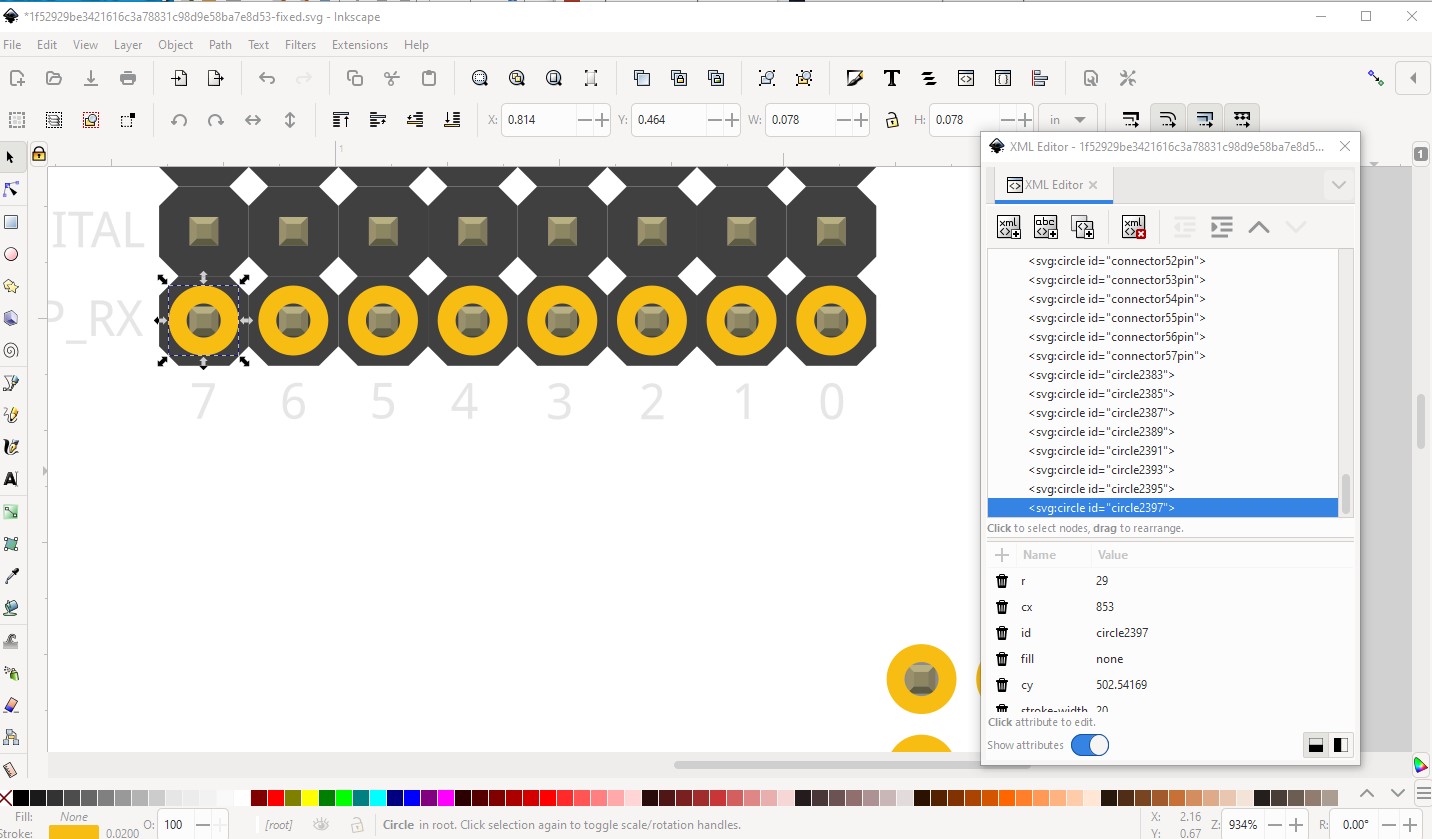
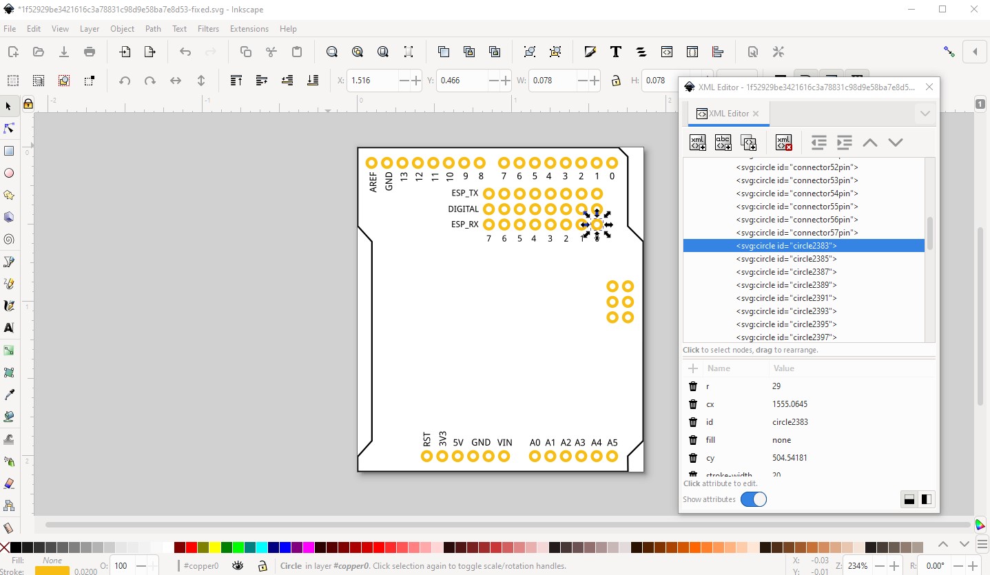
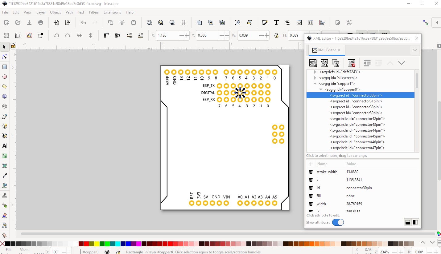
The last thing is how to handle the connectors on my “esp-header” in a group of the same name. I copied circular solder pads since I notice they are under all the headers on the board I copied from (The arduino Zero). But then I noticed, that there are already connectors on the headers I cut and pasted from the core parts. Specifically, I created connector34pin through connector57pin by copying circular solder pads under the headers. But when I look at the headers, for example group id “esp-rx” under the “esp-header” group, it has smaller connectors that also have terminal id associated with them. Would you delete the ones in the header, or should I delete mine and then use the ones inside the header? Image below:
Here is the latest version. I think something was in a different layer, because when I deleted that, I was able to finally ungroup the “breadboardbreadboard” group and come up with what I have now.
I would delete yours and use the ones in the original header. I usually also delete the terminalIds as they aren’t needed (but are added by the parts factory) in breadboard headers. You then also need to remove the terminalId field in the .fzp file for the connector.
That is odd, as it wasn’t in the posted svg. I didn’t need to delete anything to ungroup the svg you posted!
Boy this is frustrating. I thought I had everything perfect and tried to use it as a breadboard image in the Fritzing parts editor and it only sees some of the connector pins. I didn’t move them to the bottom, but ran the file through fritzingpartscheck. Have any ideas?
I am thinking it has something to to with the order the connectors are in the file and if they are in a group. Can I just pull connectors out of the group and move them where I want from the xml editor? And why does the RST connector look different that what few other connectors are appearing.
The frustrating part is my normal reaction to parts editor and thus I rarely use it! At a guess the pins that are showing up are defined in the .fzp file, those that aren’t are not. Note AFAIK the parts editor can not create connectors in the fzp file, you have to have an fzp file with the appropriate number of connectors already defined (I think with appropriate connector numbers but may be wrong there, it is possible that parts editor can change pin numbers.) You can then assign a graphic to a connector (although I never have much luck making this work) and set the terminalId via the n/s/e/w icons in the parts editor screen. I’d expect FritzingCheckPart to be fairly unhappy with this as it looks for the connectors defined in the fzp file in the svgs and it is unlikely to find them as the connector numbers don’t look to be correct in the svg.
Shouldn’t be either of those. Parts editor loves groups and creates lots of them and xml doesn’t care about order in the file it will search for what it wants. You can safely ungroup the svg and then regroup it in to only the breadboard group (that is what I usually do to avoid transforms.) As long as there is a group with the layerId present Fritzing will be happy, it doesn’t require any other groups but will deal with them if they are there.
At a guess because it is connector0pin and that is likely what the graphic is indicating. A good bet would be to check the .fzp file and see if the connectors being recognized are in the fzp file.
I suspect the connectors that are showing in parts editor have a connector entry in the fzp file (connector0pin here) and those that don’t appear don’t have such an entry. As noted the parts editor is very limited with what changes it can make in the fzp file.
I will not be defeated by Fri**zing (stars included because I now consider the name to be an expletive.
What is the best procedure to edit the files to get my pins working when starting from an existing part? Up to now, I just use an existing part that was “close” and made a “newpart.breadboard.svg” file on my desktop and then loaded it into the parts editor for the breadboard view. I keep changing it and the .fpz file and reloading the desktop file. But that may not be working. When I save the part it always asks for the “prefix”. It looks like every time I save, a new newpart.breadboard.as9s9dsss…_breadboard.svg gets created in the user folder from newpard.breadboard.svg file on the desktop I was using. So I am accumulating many versions of the breadboard files in the user folder.
Do I continue to do this working from my own .svg files and letting fritzing update them, or do I open all the files Fritzing creates in my text editor and edit those? I worry because I may have to load a file into Inkscape and the desktop file is the one I have been editing. The breadboard file Fritzing creates based on my Inkscape svg is formatted completely differently that my svg. Depending on what I need to modify, it is either easier or more difficult to find objects.
I had to add connectors to the .fpz file so that they would display in the breadboard parts editors. Everything was going well, until the last 16 or so connectors. I have a row in an 8x3 female header and was on the second of the 3 rows and the connectors jumped around. So I fixed them in my .fpz file, import the newpart.breadboard.svg file again, and 2 connectors are missing from the row I fixed before. I don’t see how my .svg file has anything to do with the connectors showing because the .fpz file is what holds those connector definitions! If I load the last version of the breadboard svg Fritzing created when I saved the part, those pins come back. But working with files that have 30 or whatever random characters tacked onto the end is a huge pain. Bottom line is I can’t see why my connectors don’t appear in the parts editor since I thought I had it all worked out and can’t find any missing tags or misspelled connector names.
What I do is documented in my tutorial, basically start from something with the correct number of pins (not necessary for me because I have a script which will generate the correct number and format of pins, that script is available here:
I copy the output of the script between the connectors tags in the fzp then edit the description and (if not preset) the name fields.
Yes to save a new part parts editor creates a new part with a new moduleId and new file names every time which leaves a mess. Editing the files directly (perhaps using parts editor once to set a new moduleId although I don’t even do that any more) is a much cleaner method in my opinion.
Other than parts editor adding a bunch of useless groups the formats should be more or less the same. As noted earlier Frizting doesn’t care about any group except the layerId and is perfectly happy if you remove them all. If you leave px on the font-sizes you may have text problems though (this is an incompatibility between Fritzing and Inkscape which FritzingCheckPart.py will fix if the svg is run through it before being loaded in to Fritzing.)
Best bet here is to upload both the svg and the .fzp file and I will have a look and tell you what is going wrong. Running FritzingCheckPart.py against the fzp file should also tell you what is wrong (it will also complain about schematic and pcb if they are not complete though!)
Thank you again for all the help. Here is my .svg file and what Fritzing created from it. My .svg file is formatted differently. Mine has all the tags nested under the tags. Fritzing modifies my file and puts things all on one line. I start with connector0pin on the lower left and go through all the headers. Then I go to the “ESP” bank of 8x3 headers from the lower left to the right (0-7), then tried to go to the middle header.
I think I have it. I am just editing the last version of the files Fritzing created in the user folders (the ones with the huge hash at the end. I realized now that every time I save, it uses a new file with a new hash, so it was working against me. There is no need to save if I am editing in the svg files directly. So I can just make the changes, then load the part in the part editor to check it. Just don’t make any changes in the parts editor. At least not yet. There were also more than one object with the same connector ID, so that was causing issues. Only the ICSP header to do and to join the pins that are on the same net. Then move on to the schematic and pcb
OK, so I unzipped the .fzpz file and ran it through FritzingCheckPart.py which details the problems (I am ignoring a bunch of warnings here that aren’t deadly and only considering errors which imply non functioning.
Error 47: File
‘part.makerfabs_wifi_a7b0ca7379158729b2a45ab7c4a39089_1.fzp.bak’
At line 55
LayerId breadboard doesn’t match View breadboardView layerId breadboardbreadboard
This is likely your main problem. It is this in the .fzp file:
here either layer breadboard needs to be breadboardbreadboard or the layer definition needs to change from breadboardbreadboard to breadboard to match the layer in the connectors. I would probably use breadboard for both as it is more standard. That repeats for all the breadboard connectors. Then we hit
Error 69: File
‘svg.breadboard.makerfabs_wifi_9f87ba5baa38121b487ca47bee14d0d2_3_breadboard.svg.bak’
At line 11
Found a drawing element before a layerId (or no layerId)
This indicates you don’t have a breadboardbreadboard layerId in the svg file (it has breadboard instead.) The only consequence of this is that the part won’t expert as an image (which is a problem but not deadly fatal!) Then we have
(which has the original breadboardbreadboard layerId)
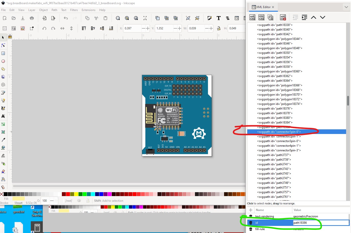
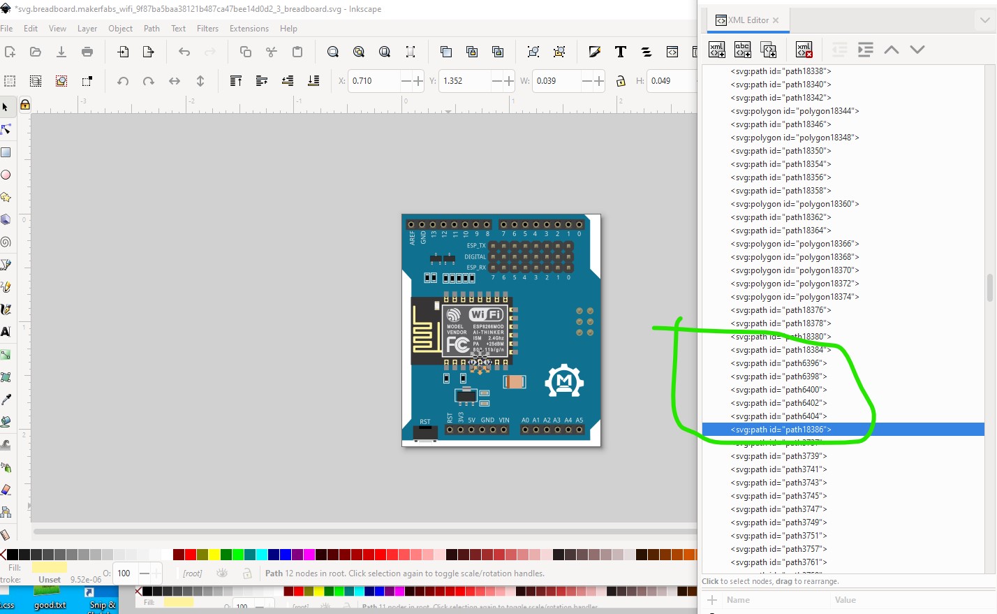
but the svg has no connector57 defined. This will cause a red rectangle (indicating missing connectors) in the Fritzing breadboard display. So I edited the breadboard svg in Inkscape and ungrouped it, them moved the connectors in pin order to the bottom of the svg. Once that was done I searched for “connector” which turns up this:
there are 5 connectors here that are not used. To avoid problems (which won’t occur if they aren’t defined in the fzp file as they are not) I replaced the id with a path like this
now I move to connector0 where moving it to the bottom has broken the image as the connector has a stroke value. There are two ways to fix this, in Inkscape just replace the stroke with none like this:
then repeat for the rest of the pins or save the svg then edit it with a text editor (vi in this case) and do a global replace of the stroke value with none like this:
I am going to change the order of the pins (and then renumber them!) in to a format suitable for the schematic extension documented here:
basically the bottom 12 pins will be on the bottom, the 6 ICSP pins and the 24 esp pins will be on the right side and the 16 top pins will be on the top like this:
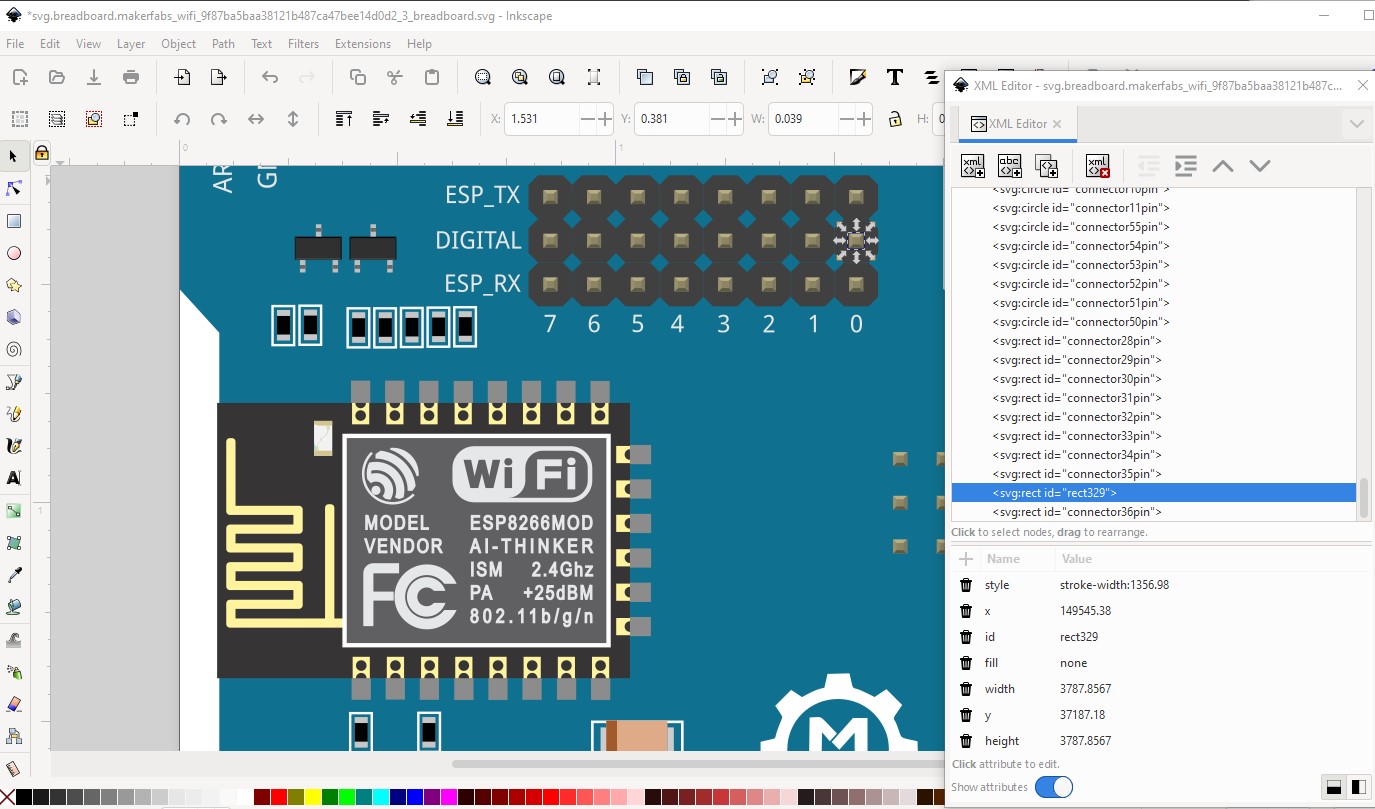
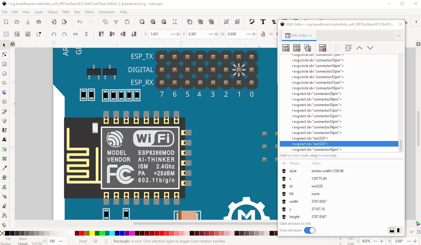
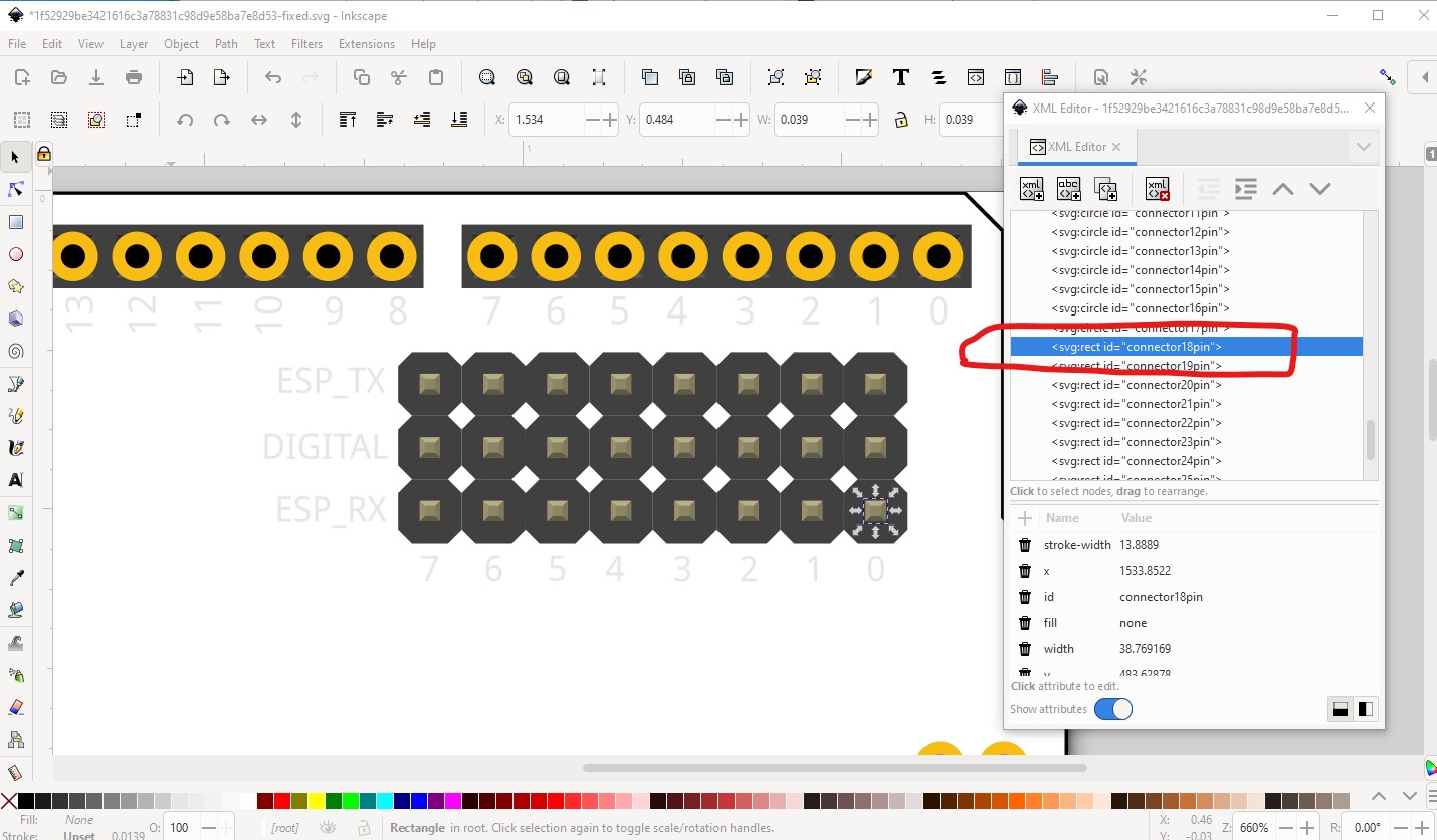
here a problem appears, we are missing two connectors on the header. It jumps over 2 pins from connector35 to connector36, so we need to define connectors for the two missing pins. To do that I select the rectangle that is the connector (it has no fill!) on the pin and move it after connector35 like this:
Now we are finished with the connectors in the correct order (if not numbered correctly) so now I save the svg, then run a script to renumber the pins. Connector0pin is the correct starting point and it will renumber from there like this (you can also do this manually by updating each id in Inkscape but that s tedious and error prone!)
Now we need to modify the fzp file to match the new breadboard svg. First we correct the layerId from
to
to match the layerId in the breadboard svg. Then I deleted all the connector definitions (I also need to delete the bus definitions below it later!) from this
as they won’t affect functionality I’ll only do connector0. Because the current bus definitions also won’t affect functionality I will ignore them as well. Now running FritzingCheckPart.py
Error 53: File
‘part.makerfabs_wifi_a7b0ca7379158729b2a45ab7c4a39089_1.fzp.bak’
At line 925
Bus nodeMember connector87 does’t exist
Error 53: File
‘part.makerfabs_wifi_a7b0ca7379158729b2a45ab7c4a39089_1.fzp.bak’
At line 930
Bus nodeMember connector88 does’t exist
but doesn’t bitch about breadboard only schematic and pcb (neither of which are corrected yet!) so we should be able to make a part that runs in breadboard correctly like this:
technically (and practically) breadboard is not correct because the fzp file needs the ICSP and ESP pins defined as female like this (which I haven’t done!)
the change from male to female means the pin won’t connect to the breadboard (where it would short!) as the breadboard pins are female. As noted the next step is to create the schematic svg using the Inkscape extension and then pcb (the easy way is to copy breadboard then delete the uneeded parts which is everything except the connectors, board outline and mounting holes) and apply the correct groups. I can do that if you like. Here is the part created above with the working breadboard and fzp files.
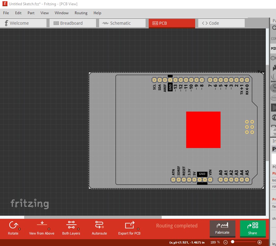
I tried to make a start on the PCB. First, the breadboard drawing has no outline. So I took the board, removed the fill, then gave it a .006" outline (not sure what the standard is, but that is what it was on the board I copied). Then I did that, it expands the board size by that amount, so I then resized the page to the board.
I found when I was doing this that somehow the board outline was not closed in the lower left vertical corner piece. I’m not sure how it filled correctly. You can see this if you look at the board in the part you fixed for me in the last message. I selected what I thought were the two open nodes, then used cntrl-j to join them and then the outline completed. What is interesting is that I can not fill that shape with anything but black after that. I wanted to fix this in the breadboard svg, but afraid of what that might do now.
I’m not sure what to do with the headers in terms of what to outline and what to delete. The breadboards I see have nice outlines around the connector (sometimes) and usually a round gold solder pad. So I deleted everything except the connectors, renamed them to “pad”, and made them the standard gold color. Is that the way to finish it up?
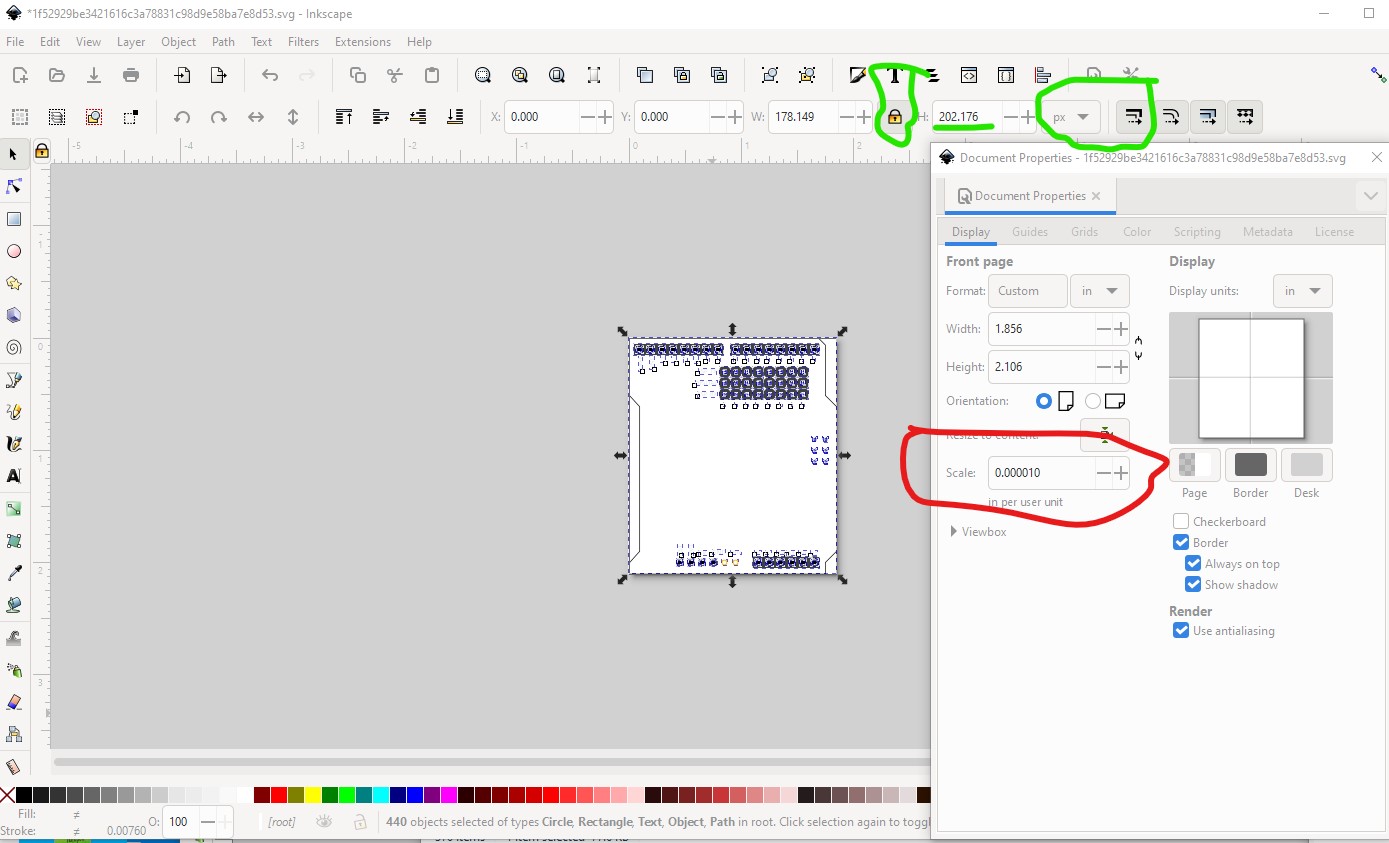
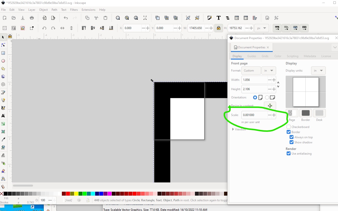
OK, first I rescaled the svg to be standard 1 drawing unit = 1/1000in like this Edit->Select all, then File->Document properties, lock width to height (keeps circles circles) dimensions to px (finest pitch) and enable scale stroke-width when scaling. Then record the largest of height or width (height at 202.176px in this case) to set later.
So the first thing we need is for all the connectors to be circles with a fill of none and a stroke of #f7bd13 with a stroke width of 20 (20 thou ring) and a radius of 29 which sets the hole size to 0.038in suitable for a 0.1in header. The calculation is
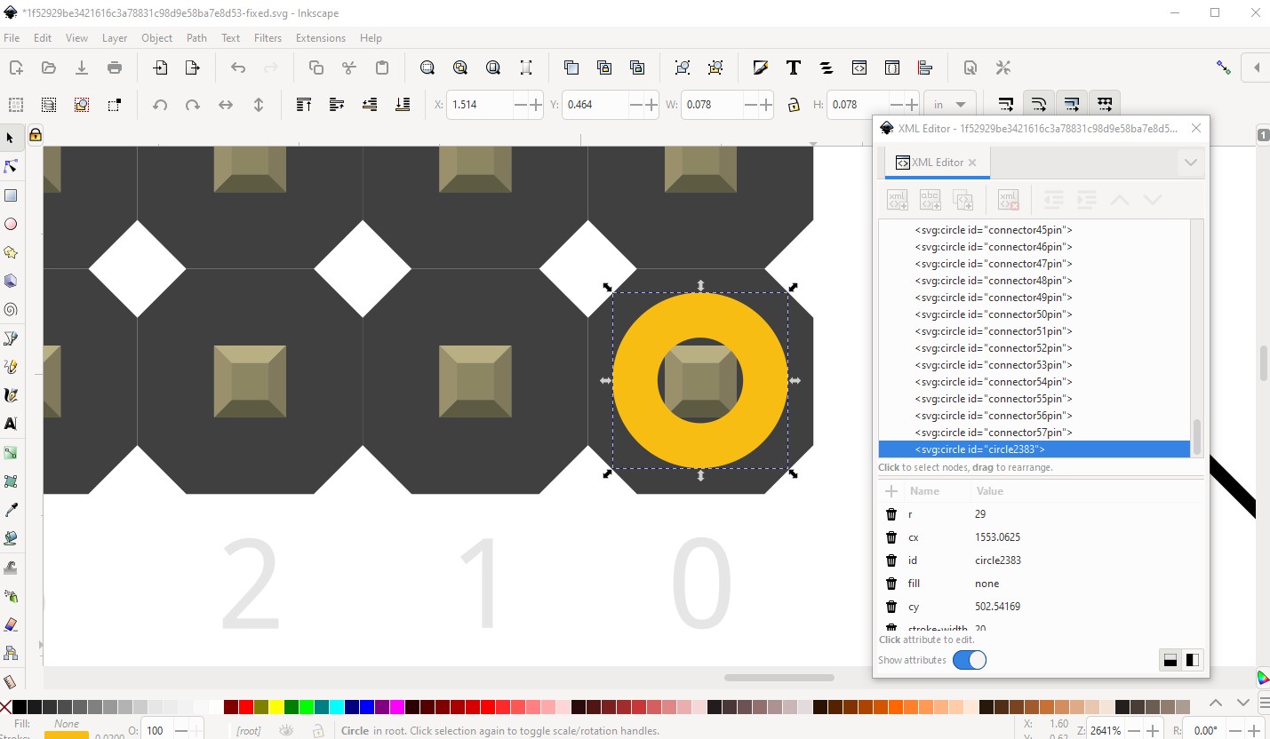
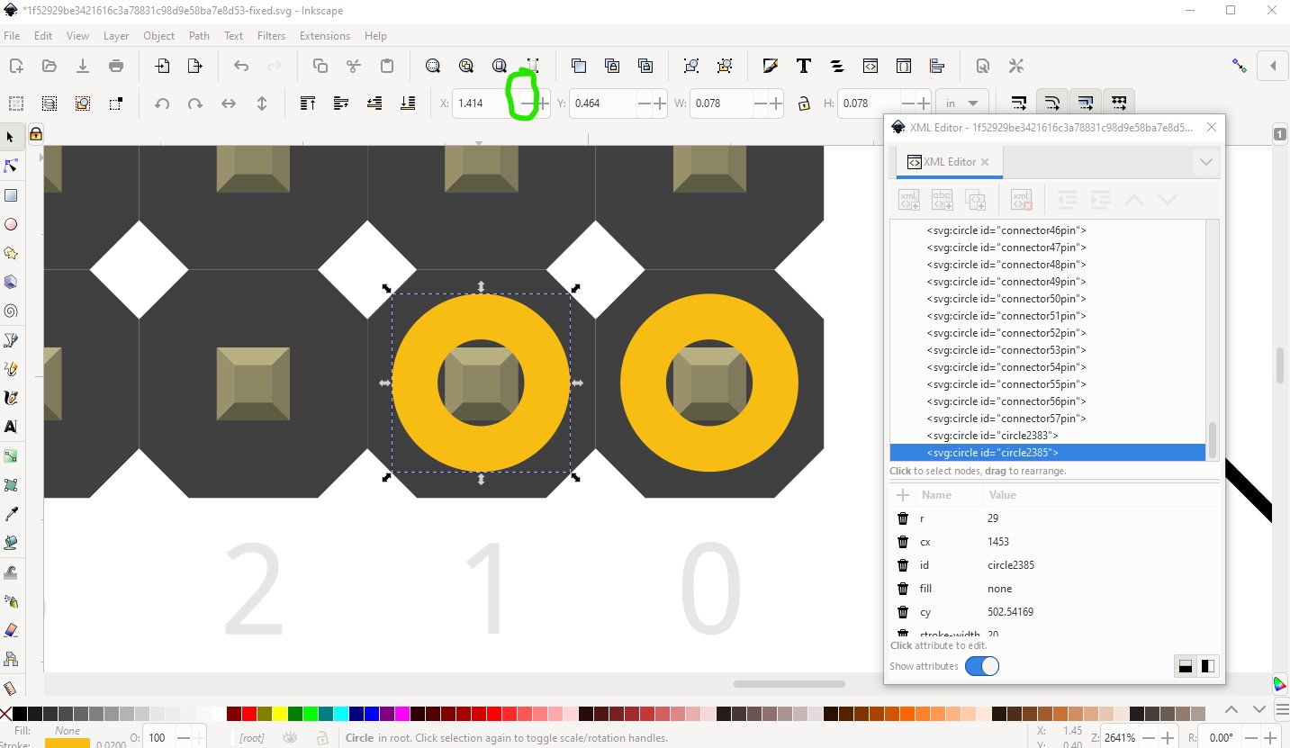
two issues here: the header doesn’t have circles (only rectangles) so we need to replace them with circles. As well there is text which usually isn’t included in pcb for a part because to remove it (if the user doesn’t want it) they need to modify the part. If it isn’t present it can be added to the sketch that uses the part if it is needed. I left the text in as I don’t know if you want it or not. Either way will work fine. Now I need to replace the header connector rectangles with circles. The easiest way to do that is to duplicate an existing circle and move it, then duplicate it and step it 0.1in to the left like this starting from here
if I had been smart (which I wasn’t!) after positioning the first new circle I would have deleted the rest of the connectors to avoid trying to do that later but I didn’t.
So now I have all the connectors (except not in the correct places) so now I need to remove all the header bits. A select box like this (avoiding selecting the gold pads!) will be easiest. Deleting this gets rid of most of the connectors
then do the same for the other headers. With that done and the text set to a fill of #000000 (black) we are ready to make the groups. silkscreen should be the top group and contain the outline and the text. In this case it is easiest to add the text one at a time to the silkscreen group (because a select will get connectors which we need in another 2 groups!) starting from here
Note the Part1 indicates I missed adding a field to the fzp file to set a label (which it should have!) setting
<label>A</label>
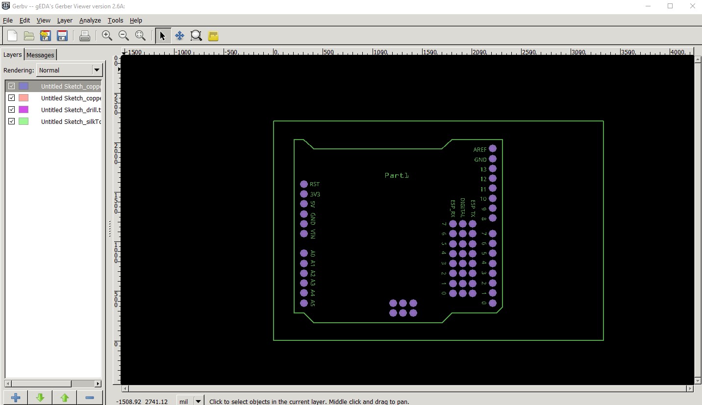
somewhere in the .fzp file. That will set the part type to A (for assembly it being a board!) will fix that. Welcome to the complexity of making parts! Note it is a good practice to export the part as gerbers and check the hole sizes in the drill.txt file (here the correct 0.038in)
; NON-PLATED HOLES START AT T1
; THROUGH (PLATED) HOLES START AT T100
M48
INCH
T100C0.038000
%
T100
X022106Y019376
X003106Y005797
X022106Y018376
X013101Y002771
and that everything appears in the gerbers (there are some problems with paths in gerber output sometimes although I think they are mostly fixed now!) This is the gerber output displayed in gerbv
Wow. I’ve been through your tutorials and some other messages where you helped others. I think the spaced repetition of some of the steps is helping. I’ll put it in a document I can reference.
Can I name the files what I want and put them in the .fzpz? I know the .fzp file references a name, but not sure I need to have them all have that huge hash at the end of them. I am guessing I can take the pcb file you fixed and just cut and paste it into the .svg file that has the same has as all the others? IOW, I now have pcbabdcef and you made pcb12345. I could either rename yours or cut and paste into mine.
Now back to the schematic. I’ll give that a whirl with the Inkscape plugin and follow your tutorial. Taking a day off from this tomorrow to take my daughter to an amusement park Halloween scare night.
On to what I hope is the final piece of the part, other than a few mods to the .fzp file, is the schematic. Is this good enough? I wondered about the pin numbers. On the breadboard, the digital 0 pin is pin 43, connector42. So I have it as connector42pin and connector42terminal on the schematic. Is that correct?
The other issue is how to handle a strange board like this regarding the ESP headers. The way the board is supposed to work is that ALL the TX pins are tied together, all the RX pins are tied together and go to the single TX and RX pins on the onboard ESP8266. And the digital row is just an extension of the digital 0-7 header except with male pins. You are supposed to use jumpers so that a jumper from the #2 digital row down to ESP_RX 2, for example, connects the ESP chip Rx input to pin 2 of the Arduino it is snapped onto. And you do the same by connecting the TX pin of the ESP vertically up from whichever digital pin you want so any of the Arduino pins can be used as a serial transmit or receive pin. I don’t know how to model that. Do I need to still all those pins on the schematic?
What is more complicated, and why I only showed the 2 ESP pins on the bottom of the schematic is because we don’t use the board that way. We remove the 2 jumpers and bypass the connection to the Arduino header and run a jumper wire from any of the RX and TX pins to one of the extra, not connected to shields, serial ports on an Arduino Mega. Another way to look at it would be that I am jumpering the TX and RX pins of the ESP8266 to something off the board and using the header pins because they are convenient. I’m not sure, even in that case, if I should show the other 7 pins on each of the ESP headers, since you could connect to those. As a shortcut I just used the first (0) pins of the ESP_TX and RX header rows (connector18pin and connector34pin). I hope that is clear. What are your thoughts?