Fritzing SVG dimension rules

Hi,

I’m struggling to create svg for new parts. Some of the issues I face are scaling problem, pin alignment on the grid, dimension issues, …
I code svg as an xml file with an IDE using inches or metric system.

So far I didn’t found any information on how to deal with dimensions, positioning, scaling, … in Fritzing ?

Do someone knows where is that info or how to do ?

I’ve got vids that tell you how to draw stuff, but it doesn’t help if you go the XML code way.

My guess is get a svg out of FZ and see how they do it. Just edit part, and File/Show in folder, for that view.
Otherwise upload that svg here with the 7th button above.

Helpful Info:

• SVG’s are based on XML
• XML native default units are PX (pixels)
• XML units can be coded for all units
• Results of the SVG (and XML) depend on the DPI of your display and Rendering App. Typical are: 72 DPI, 90 DPI, 96 DPI…
• Settings for correct result requires some homework

• With:
• knowledge
• one resulting output
• DPI known (or guessed). Remember, DPI=Dots-Per-INCH. Which is the same as saying, ‘Pixels-Per-Inch’
The scaling is calculated then coded into the XML

Example
Given:
• a Rectangle in SVG with dim’s of 100mm (3.937in)
• for 72 DPI, the Pixel setting is:
(3.937in)(72px/in) = 283px

• for 90 DPI, the pixel setting is:
(3.937in)(90px/in) = 354px

Example, for Metric(mm) with syntax as noted above:
(283px)(in/72px)(25.4mm/in) = 100mm

Now, armed with info, Make a 46x48mm Rectangle for a PCB SVG in the XML with Layers/etc for a Fritzing PCB.

  • If you do the calc’s to solve the Fritzings ‘Pixels/inch’, you 'll see it’s 90DPI (for older Fritzing, don’t know about new version, i don’t use it).
    X = (25.4mm/in)(163px)(1/46mm) = ?

Example
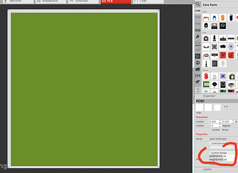
• Below Fritzing shows Width=46mm, Height=48mm
• XML shows 163 x 170 px (rounded)

The attributes on the initial wrapper svg element actually set the units and scaling to use for the file.

<?xml version="1.0" encoding="UTF-8"?>
<svg
  xmlns="http://www.w3.org/2000/svg"
  xmlns:xlink="http://www.w3.org/1999/xlink"
  version="1.2"
  baseProfile="tiny"
  x="0"
  y="0"
  width="1in"
  height="2in"
  viewBox="0 0 1000 2000"
>

In the above, the width and height attribute values specify the physical world dimensions and units for the file contents. the viewBox shows the matching internal pixels used to cover that area. So for this example, the image is 1 inch by 2 inches, with 1000 pixels per inch. Or 1 pixel = 1 mil. In the above, the x and y attributes are optional. The default is 0,0. For Fritzing, they must be 0, 0, and so must the first 2 values for the viewBox.

Most of the svg drawing tools default to using something close to video screen units. Like 72, 90, or 96 pixels per inch. Different versions of the the same program can use different relationships. Some will use “px” for the units, so the relation becomes 1 to 1. That does not work well for Fritzing, because it then has to guess what the relation is between px and real world units, to be able to match up with things that have real dimensions. Different programs have different ways to specify the units to use. With varying levels of difficulty. Most will honour the units that are already in a file when it is opened.

For an existing svg file, you can determine the scaling easily. Take the last number in the viewBox, divide by the height will give the number of pixel per the unit on the height. Which should be the same as (very close to) the second last number divided by the width.

When generating my own xml/svg, I go with mils. 1000 px per inch. When the units for the part are specified in mm, and I do not have a GOOD reason to convert, I go with 100 px per mm. Those are just for convenience, because it becomes easy to calculate most of the coordinates, stroke, font sizes, etc. Anything in the images that corresponds to physical world dimensions.

If your part uses a filled shape, without a stroke, as a background over the whole area for the part, it needs to have a minimum coordinate of (0,0), and the viewBox extent will match the maximum coordinate in the shape. If the outer edge is using lines with a stroke instead, the minimum line coordinate needs to be 0.5 * the stroke width, and viewBox extent will be the maximum coordinate + 0.5 * times the stroke width. Of the specific svg elements at the edge of the image. The stroke width extends half its size each side of the specified coordinates, and that needs to be included in the viewBox extents, or the image gets trimmed on viewing. That includes stroke effects, like rounded ends on the lines. You need to watch text that gets close to the edges. It is very easy to get it truncated on viewing. It happens on Fritzing svg exports regularly, when labels are above or the the right of the top and right parts in the drawing.

When working with xml directly, I often manipulate the viewBox, height and width values. Adjusting them can zoom and pan the image to check details in the viewer program. Just be sure to reset them before using to create a Fritzing part. One simple trick, is to (temporarily) multiply the width and height by 10 or 100. That gives a 10 or 100 zoom on the image, which helps when the whole image is really less than an inch. The viewBox values specify the starting coordinate and extent (relative width and height) to display in whatever window is being used to view the image. Changing the first 2 pans the image, the second 2 zoom. Try to keep the aspect ratio (width/height) somewhat close to reality, or the view may not be what you expect.

Thanks for all these information.

What about positioning ?

Actually I have a shape with pins not aligned on the grid.

Fritizing will (from experience, I do not see any documentation for this) pick one pin from the (view for a) part as a reference point aligned with the current grid (when the part is placed or moved with align to grid turned on). I have found no consistency about which pin gets chosen. The same part can use different pins in different sketches.

The only way I know to get your symptoms, is to have at least one pin that is not aligned to the same grid as the rest. Or maybe have the grid size set to an odd value. In breadboard and pcb view, that happens for parts that have pins that physically do not all align to a single grid. Like the Arduino UNO boards (and shields). Schematic view should always align. If it does not (and grid size is correct), it is an error in the way the part was created. For schematic view, it will be the center of the “terminalId” elements that are matched to the grid. When they exist, and are linked properly in the fzp file. Otherwise it is the center of the “svgId” elements, which is normally a line. If there is a mixture, and the lines are (for example) 0.1 inch long, then the alignment will shift back and forth by 0.05 inch.

Which view (or views) is the alignment not working for?

With a sample image we could check for obvious alignment coordinate issues. A complete part file is needed to check what coordinates Fritzing should be using for the alignment.

There also seems to be something with the page size, at least in SCH. :slightly_smiling_face:

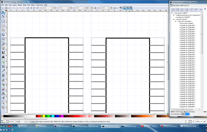
I made this SCH drawing and did, select all, resized the page to the selection, ie, everything is now ½ a grid off, and assigned the anchor points to the tips. And and you can see the part doesn’t snap the pin to the grid perfectly, but snaps to the indicator colour of the pin.
offset pin colours.fzpz (6.6 KB)

This is the same drawing, but the page size is through the centres of the line stroke.
perfect centerlines.fzpz (6.4 KB)

From the svg header of svg.schematic.test-boarder-anchor points_085f329dc2d1b8069db54d0d0c5b88c3_1_schematic.svg (from the “offset pin colours.fzpz” part) you have the drawing set to 25.4 pixels per inch. Or the px are mm.

<svg xmlns="http://www.w3.org/2000/svg" width="1.01in" id="svg829" gorn="0" height="5.2119999in" version="1.1" viewBox="0 0 25.653999 132.3848">
  • 132.3848 / 5.2119999 = 25.400000487336925
  • 25.653999 / 1.01 = 25.399999009900988

With that, extracting the connector terminal rectangles (the only elements that should be expected to align to the grid)

<rect stroke-width="0" id="connector0terminal" fill="none" width="0.010668" y="2.38735" height="0.000508" x="-0.259334" stroke="none"/>
<rect stroke-width="0" id="connector1terminal" fill="none" width="0.010668" y="4.92735" height="0.000508" x="-0.259334" stroke="none"/>
<rect stroke-width="0" id="connector2terminal" fill="none" width="0.010668" y="7.46735" height="0.000508" x="-0.259334" stroke="none"/>
<rect stroke-width="0" id="connector3terminal" fill="none" width="0.010668" y="10.0073" height="0.000508" x="-0.259334" stroke="none"/>
<rect stroke-width="0" id="connector7terminal" fill="none" width="0.010668" y="2.38735" height="0.000508" x="25.3947" stroke="none"/>
<rect stroke-width="0" id="connector6terminal" fill="none" width="0.010668" y="4.92735" height="0.000508" x="25.3947" stroke="none"/>
<rect stroke-width="0" id="connector5terminal" fill="none" width="0.010668" y="7.46735" height="0.000508" x="25.3947" stroke="none"/>
<rect stroke-width="0" id="connector4terminal" fill="none" width="0.010668" y="10.0073" height="0.000508" x="25.3947" stroke="none"/>

Shows that they are NOT aligned to a 0.1 in (2.54 px) grid in the x dimension. All of the width values are the same, and all of the height values are the same. Different from each other, but still consistent. So the actual alignment point will be offset from the x,y coordinates by half the width and half the height. That will be exactly the same for every connector, so can safely be ignored for checking coordinate spacing. For the same reason, the translate in the outer group element can be ignored.

  • 10.0073 - 7.46735 = 2.539950000000001 = 0.1in
  • 7.46735 - 4.92735 = 2.54 = 0.1in
  • 4.92735-2.38735 = 2.5399999999999996 = 0.1in
  • 25.3947 - -0.259334 = 25.654034 = 1.01in

That means that (based on my description), Fritzing will choose either -0.259334 or 25.3947 px as the (grid alignment) reference point for that direction. One edge will be on the grid, the other will not. The page size has nothing to do with it.

For svg.schematic.test_26bad7d82afd69b8badfe10dda84d875_1_schematic.svg (from the “perfect centerlines.fzpz” part)

<svg xmlns="http://www.w3.org/2000/svg" width="1in" gorn="0" id="svg829" version="1.1" height="5.1999998in" viewBox="0 0 25.399999 132.08" >
  • 132.08 / 5.1999998 = 25.40000097692312
  • 25.399999 / 1.1 = 23.090908181818182

The px size is actually different in the x and y directions. Which makes the calculation of the grid spacing more complex. I have never worked out in detail how Fritzing will handle that situation. I would hope it scales the x and y differently to adjust. It might just pick one. The id="silkscreen" element is another issue. Assuming that gets treated properly as the “schematic” layer …

<rect width="0.010668" y="2.53975" stroke-width="0" x="-0.132334" stroke="none" gorn="0.2.0.0.0.0.0.0.0.0.0.2" id="connector0terminal" fill="none" height="0.000508" />
<rect width="0.010668" y="5.07975" stroke-width="0" x="-0.132334" stroke="none" gorn="0.2.0.0.0.0.0.0.0.0.0.4" id="connector1terminal" fill="none" height="0.000508" />
<rect width="0.010668" y="7.61975" stroke-width="0" x="-0.132334" stroke="none" gorn="0.2.0.0.0.0.0.0.0.0.0.6" id="connector2terminal" fill="none" height="0.000508" />
<rect width="0.010668" y="10.1597" stroke-width="0" x="-0.132334" stroke="none" gorn="0.2.0.0.0.0.0.0.0.0.0.8" id="connector3terminal" fill="none" height="0.000508" />
<rect width="0.010668" y="2.53975" stroke-width="0" x="25.5217" stroke="none" gorn="0.2.0.0.0.0.0.0.0.0.0.56" id="connector7terminal" fill="none" height="0.000508" />
<rect width="0.010668" y="5.07975" stroke-width="0" x="25.5217" stroke="none" id="connector6terminal" fill="none" height="0.000508" />
<rect width="0.010668" y="7.61975" stroke-width="0" x="25.5217" stroke="none" gorn="0.2.0.0.0.0.0.0.0.0.0.60" id="connector5terminal" fill="none" height="0.000508" />
<rect width="0.010668" y="10.1597" stroke-width="0" x="25.5217" stroke="none" gorn="0.2.0.0.0.0.0.0.0.0.0.62" id="connector4terminal" fill="none" height="0.000508" />
  • 10.1597 - 7.61975 = 2.539950000000001
  • 7.61975 - 5.07975 = 2.54
  • 5.07975 - 2.53975 = 2.5399999999999996
  • 25.5217 - -0.132334 = 25.654034

The px deltas are the same as before, but the scaling to real world units (inches) should be different.

All of that is totally separate from the offset (or lack of offset) between the actual connectors (as defined by the connectorNpin and connectorNterminal elements) and the background graphics that look like connector terminal lines. Which is simple delta coordinate values, nothing at all to do with (connector pin) alignment to grid.

Side Note: FritzingCheckPart says that the pcb view silkscreen for both parts is white, and should be black.

EDIT: Further research shows that the offset from grid is probably because the connector terminal elements were placed at the tip of the curved arc (stroke-linecap:round) at the end of the connector pin elements. Those should instead be placed at the center point of the arc, which is the same as the end point of the connector pin element when the linecap is set to ‘butt’. The linecap graphics extend beyond the end of the element coordinates. Which increased the distance between the rows of connector terminal elements by the width of the stroke for the connector pin lines (path elements), half the stroke at each end.

I never use px in INK and always set it to mm or inch at the start. And I don’t have a chance with code. Whatever it did was internal in INK.

It’s the same drawing in both, just one where I manually resized the page to cut through the centre of strokes, the other I resized the page to the drawing, ie, the max outside of drawing.


Here is the link of the 2 drawings -

Pin assignment was inside FZ Edit. It doesn’t matter if the part has connector#terminal in the svg or not, it does the same either way.
page size.fzz (28.8 KB)

EDIT
I really don’t understand how I’m drawing it wrong, when literally this is the only way to draw a rectangle and 100 lines in INK.
Here is a vid of how I did it, if you can point out what is wrong.

*Video deleted because it was updated, so I’m removing this from my YT channel *

I don’t know what is up with that, but if I get the svg from inside FZ Edit/show in folder, it gives me the correct drawing. But if I select File/Export/Image/svg I get blank svgs.

What do you think is the difference between “the pin” and “the indicator colour of the pin”? When I tried those initial 2 part files, they both aligned the schematic connector terminals from one row of the pins to the drawing grid (set to 0.1 inch). The other row did not quite align, due to the terminal elements not being a multiple of 0.1 inch from the first row. I also saw the shift of the background (grey/black) graphics relative to the connector pins and terminals in one of the parts. Which has nothing to do with aligning to connectors to the grid. The ONLY thing Fritzing will attempt to align is the connectors, based either on the terminal graphics (when they exist) or on the pin graphics. Everything else will be positioned relative to that reference.

What do you mean when you say “the page size is through the centres of the line stroke”? I do not understand how size and line stroke position are related. Which line stroke? the connector pin lines? The non connector lines?

Is this partly an issue with the older version of Fritzing I think you are using?

If Inkscape breaks the svg files, then Fritzing can not do anything about it. Is it a Fritzing or Inkscape problem you are seeing?

Separate note, that SHOULD not have any effect: Why are you using path elements instead of lines for the connector pins?

For the schematic view? That will happen if the layer name for the view does not match the name in the fzp file. I mentioned earlier seeing “silkscreen” where I expected “schematic”. Frtizing only exports the graphics content from the svg element that matches the layerId specifed for the view in the fzp file.

  <schematicView>
   <layers image="schematic/test_26bad7d82afd69b8badfe10dda84d875_1_schematic.svg">
    <layer layerId="schematic"/>
   </layers>
  </schematicView>
<g gorn="0.2.0.0.0.0.0.0.0.0.0" id="silkscreen" >

That schematic svg does not contain a “schematic” id, so nothing will export. The content is still shown in the Fritzing view, and usually works fine, but will not export.

I researched this 2 months back and it seems ‘line’ in an Illustrator thing, and that INK only does path for a line.

What it seems like is INK is junk, and FZ is too pedantic.

If INK doesn’t add a schematic” id I can’t do much about it, because I can draw, but I’m not going to know if code is missing, ie, like every beginner.
And when you have 2 identical drawings with pins and terminals assigned the same way in FZ Edit, and 1 is perfect, and 1 is offset, that’s even worse. If INK is putting out 2 different svgs based on the page size, it’s going to be impossible for anyone to be consistent in making parts.
If you grab the SCH out of a 100 pin FZ part and look at the XML, no beginner is going to make a part with that many elements, ie, line, connector#pin, and connector#terminal, for every pin - that’s 300 objects alone -. And if people need to be at such a high level of XML coding to make FZ parts, they would go straight to KiCAD because FZ would seem to basic. Basically part making for a beginner is untenable at a FZ level.

The way I draw it is the same way every beginner is going to do it, ie, set 0.100" grid in INK, snap a rect to grid, and snap 100 lines to the grid - this is exactly how it’s done in KiCAD -, and if that’s not acceptable for FZ, it’s too much for beginners. It kind explains why there isn’t detail instruction in FZ for part making, because it’s a 100 step process. :slightly_smiling_face:

Time point 3:55 “Fritzing uses the page size as a snap point”. I do not believe that is true. Or not quite true, depending on terminology used.

Time point 4:12 “Fritzing uses this corner of the page for the zero zero snap point for a part”. Maybe, but SHOULD not be related to the grid alignment point. See below.

I believe the difference between pin status colour, and no colour is “just” whether the pin is defined as male or female in the fzp file. Male pins get the status colouring when not connected, female pins do not.

I would not cite the existing core parts as a reason to use a specific style schematic symbol. Many are very old, and were created before the current standards and guides were set up.

The information I have, “2. Schematic View Graphics” in Fritzings Graphic Standards, shows that the connector pin lines should be 100 mil, not 200 mil long, and the stroke should be 9.7 mil.

That same reference shows the pin color as "dark grey (#555555 or rgb(85, 85, 85)), which is not one of the base Inkscape grey colours. 60% Grey is #666666, 70% Grey is 4d4d4d. Need to go the Stroke Paint tab of fill and stroke to set it correctly. Either directly as 555555ff in the RGBA box, or as 85,85,85,100 in the R, G, B, A sliders and boxes

Exploring your video and Inkscape gui, I see why you have path elements for the pin lines. Inkscape does not seem to have an option to create svg line elements.

Instead of manually drawing the first few pins, I used ctrl-c to copy the first one, move the pointer to where to place the next, ctrl-v, move mouse pointer, ctrl-v, repeat. The pointer is the center of the placed selection, adjusted by the current snap rules. The same works for cloning the block of 5 multiple times. One copy with multiple pointer moves and pastes. Duplicating the larger blocks that way would be harder, because of the need to figure out where the ‘center’ of the pasted block should be.

Placing the connector terminal rectangles using Inkscape snap to grid is not quite accurate. Experimenting shows that the snap point (grid intersection) is the top right corner of the rectangle (when drag moved). Since Fritzing uses the center of the rectangle as the connector snap point, that will shift the graphics by half of the rectangle height and width. At small rectangle sizes, the error will be minimal. I think that could be compensated for by settings an offset for the gird. Change the “Origin X:” and “Origin Y:” to half the rectangle size in each direction. Not explored for this sample. What I did, was create a 0.1in square rectangle using the snap to grid, then lock the aspect ratio, and change the width to 0.001in. After that, drag (and snap) the tiny rectangle to the grid intersection, then start duplicating it (select it by clicking in the xml edit window). For the sample, I copied once then pasted 9 times, moving the pointer near the target grid intersection before each paste.

I found a way to duplicate (and exaggerate) the symptoms you saw with the offset between the Fritzing connector status colour and the line (path element) for the pin. The exaggerate was done by adding a deliberately off the grid graphic element at the top left of the drawing file before resizing to selection. That moved the coloured line further from the connector pin line. It appears that the coloured line is positioned at a grid size multiple from the corner of the svg image, which is not where it appears in the svg file. I have not seen this before (probably) because I use the other style of part, which also includes connector pins on the top. That makes the grids line up, instead of being off by half the stroke thickness of the part ‘body’ rectangle. I also ‘got lucky’ with some non-ic parts I did, because the tips of the connector lines (and associated terminal elements) happened to align to the top and left edges of the drawing.

This looks like a Fritzing bug.

This not related to the page “size”. It (from symptoms) is the offset from the corner of the page (0,0 origin) to the connector terminal elements. At the scale I did things, I can not tell if that is to the corner or center of the terminal rectangle. The Inkscape ‘fit’ operation causes the problem when the resulting top or left edge does not correspond to a multiple of 0.1 inch from the terminal rectangles. In my test, both were forced away from the grid, resulting in the coloured line moving both up and to the left from the actual line in the svg file (after rotating the part to vertical orientation, and moving to align to grid).

@vanepp, have you seen symptoms like this? I should be able to (re)create a simpler failing part. An 8 pin IC schematic should be fine for demonstrating. Even 2 pin. This COULD be tied to something that Inkscape is doing to the svg file. I should see if I can replicate the symptoms with a manually created svg file. It should be as simple as adding a translate to force the connector terminals away from the grid relative to the svg image origin (and adjust size and extents to match). Adding an extra element to the top left will make that delta more visible.

Quite possibly. Path works (or should work) fine. It was just unexpected with I have worked with before.

The ‘code’ is just the name for the layer. Or more correctly, the id for the group. In INK layer is just an svg group (g element). There is no way for INK to know this is supposed to be a schematic for Fritzing. It just another drawing file. Changing “layer1” to “schematic” should do it. Potentially, the part editor might be able to fix that, if it were made smarter. It knows what the svg image is to be used for.

The page size (height, width, view extents) are all part of the svg file itself, so yes the files are going to be different. Not much, but definitely different. The only thing that needs to be different, is the attributes in the main svg element. INK seems to randomly change the order of attributes of (all) elements during save, so other (not important) differences are likely. Just enough to make a direct comparison very difficult.

Nothing I said should have implied the need to edit svg files as xml to get proper Fritzing parts. If this problem is what I think it is, I can create the same symptom you saw with the INK created svg with one created through xml. I can also probably describe a ‘fudge’ to use in INK that will avoid the problem. The tool used to create the file is not the problem. It is the interpretation of that file. We seem to be getting an offset where there should not be one. As far as all of those elements when creating directly with xml, it is quite possible to do copy and paste there too. I do it all the time, then use global edit to adjust coordinates for the duplicated blocks. Usually in blocks of 10, so a single digit of the coordinate needs to be changed. Though I agree that a beginner should not try to start there. I worked with xml long before I ever tried to use it with svg and fxp files. Someone that has worked with (html) webpages has a head start. html is very similar to xml. html is actually based on a version of xml.

Now that we have some idea of what causes this particular problem, Peter’s validation and fixing script can probably be enhanced to avoid it, and the part editor could have the same change added. Or (better) the main Fritzing app should be fixed to not add that incorrect offset.

When I did the vid 2 weeks ago I thought it was correct, because it worked perfectly. Then I found this post, and now it’s a big mess again. Hence why I pulled that vid.
When I started checking FZ part snapping in BB and PCB views, yes the page size doesn’t seem to make a difference, but it did seem to in SCH until we found out it was an INK thing.

Don’t worry about FZ rules, because FZ CORE parts don’t even follow it’s own rules. :slightly_smiling_face: It’s own generated generic IC has 0.013" rect and 0.010" pins that are 0.200" long.

I tried it and can’t get it to work that well, plus it’s a bit harder and slower. I have to think what is easier for a beginner, and snapping is easier.

Not snapping to grid is too hard. You can use the internal FZ Edit pin assigner, if it would put the terminal in the right place. :slightly_smiling_face:

Or it’s too pedantic. :slightly_smiling_face: Like if it’s ignoring the page size, why doesn’t it take the pin as 0,0 to put it’s terminal there.

If FZ is ignoring the page size, technically they should be the same, if INK wasn’t making it different. :slightly_smiling_face:

At the moment it all just seems like a Catch22. You can’t use a graphical editor because it’s not accurate enough to make all parts to one standard of code. And you need a couple of years to get good at XML code. And even then you can’t make the code to a FZ standard when the code standard is not published anywhere. :slightly_smiling_face:

If there isn’t a simple way to make parts in FZ, FZ is dead in the water, because KiCAD/etc has simple part making, and is exactly like how I show as method #1 in my vid, ie, set grid and snap lines to it.

I asked the experts 4 years ago if they would do tutorials, but no one was interested. I even said I’ll do drafts and all they have to do is correct them, but no one was interested. So it’s a bit ironic that someone who doesn’t know what he’s doing, but can cobble something together, makes tutorials :slightly_smiling_face:, ie, because no one else wanted to do it.
5 years of a moving playing field, because there is no absolute instructions, makes me wonder why I try to promote FZ :rofl:

I usually solve this by doing a copy/paste from an svg with a line (from IIlustrator). Ink will take and modify a line just fine, it just won’t create one.

I think you are likely to have problems with this. I always use the resize page to the drawing because that sets the viewbox correctly. If I don’t do that I sometimes get line offset on the grid ( and doing the resize corrects it!) That said, how I do the above is to start from one of the schematic templates in my series of posts (the simple one for this type of schematic, it doesn’t need the additional internal groupings that the complex version has) and then delete/duplicate the lines to get the image (which has the correct scale and .1in long pins) to get the number and position of the pins I want. Then I xml editor I move the pins and terminals to the bottom of the svg and set the id of connector0. At that point I run a python script (that I haven’t released yet) that numbers the pins starting at the first “connector” it finds in sequence til the end of the svg. I’ll do an example of this part and post it so you can see what I mean. Then I have a python script that will produce the connectors boiler plate xml (with blank name and description fields) to substitute in the the fzp file. With that in place just add in the name and description fields and you are done (the same can be done for the breadboard as well.) I also have a python script (that needs more work) that will let you either renumber or add a block of pins to an svg formatted this way (all connectors on the bottom of the svg.) It makes things much easier on large parts.

I think Old_Grey is on 0.9.3 which should be pretty much identical to 0.9.4 or 0.9.5 in this area. I have never been able to figure out how pin alignment actually works :slight_smile: though.

Ink doesn’t know anything about “schematic”. You at the end of the svg editing need to resize page to drawing then edit select all and group and name the group schematic. Parts editor will do that for you (probably nested in side a bunch of numberic groups) but Inkscape doesn’t know to do that.

AFAIK grid alignment takes a pin (theories varied from always pin0 to the closest pin to the 0 0 drawing coordinates but testing tells me that neither is correct!) A few years ago I made a test svg with 4 pads on the .1 grid and then move the pads one at a time off the grid (i.e. move connector0 from .1 to .15) to try and see what pin it was using as the base. The results make no sense, no one pin appeared to be the defining pin. It looked to me like there was a vote (most of the pins are on the .1 grid so use that), but Kjell mentioned that he thought it more likely there is a floating point comparison bug somewhere (which actually makes more sense than a vote!) that causes the odd alignments. I mean to trace the code one day and find out how it decides where to position the grid, but as usual tracing it is hard. I think we will find there is a bug of some kind somewhere.

I agree, the graphics standard should be what we use. The parts factory however generates incorrect scale svgs ( for at least headers) and in schematic generates the .2 in pins (which in turn is tied in to the text placement when editing pin labels.) I have code to fix the scale problems and can fix the .2in pin length, but that will likely break pin label editing (which is also already broken though :slight_smile: ) and there is code for dealing with older IC and header formats which will make this even more complicated. I’ll probably try making some minimal changes (the svg scales for instance) and see if that can be done without breaking backwards compatibility as a complete solution which would involve adding labels for the text of pins so pin editing doesn’t need to know the x/y location of the text and adjusting svg scales and pin sizes while allowing the option to upgrade from the old format to the new one is going to be more complex.

This is a python feature :slight_smile: python exports the hashes in random order which causes this. I have considered (and may yet do) changing check/fixpart to sort the xml in to a lphabetic format so that a diff of two pretty printed svgs would actually work (it won’t at present.) It shouldn’t be that hard to do the xml is in a large text object during pretty printing and being able to do diffs would be very useful.

That is the problem in a nutshell, a lack of interest (and/or time) by the folks that can do the work. Even 4 years ago (about when I started with Fritzing) development had stopped. The conversion to open source hadn’t gone as planned and folks were losing interest and documentation is always the least attractive task to do :slight_smile: . Since then we have lost more and more of the folks with the knowledge and it is going to be hard (but I hope not impossible) to get it back. Progress is being made. Kjell has made giant strides in terms of updating the forums and the web site (which have been largely invisible to us but a huge amount of work in the background.) 0.9.4 was released, which by updating the libraries in use buys us more time before Fritzing dies of outdated libaries to make progress. It isn’t as fast as I would like, but it is still happening.

For me, the reason is breadboard. As far as I know Fritzing is still the only package (other than tinkerbox? which is an Autodesk closed source cloud based product) that has breadboard view. That is useful to me for what I typically do and reason to keep working on Fritzing (and because it is open source, I can work on it even if I can’t distribute it …)

Peter

We need KISS, because the more convoluted we make the instructions the less beginners will try it. If you look at my BB drawing vid I do the “px” correction in INK saving one step.

There is a fzz sketch here that shows “resize page to selection” in INK breaks FZ, ie, INK offsets all the coords by half stroke and that moves pins in FZ.

The svg is from scratch, and lines are snapped to a grid - the easiest way -. There is also a vid showing this in the above post.

Yeah, I snapped Arduinos to grids yesterday and snapping was all over the place.

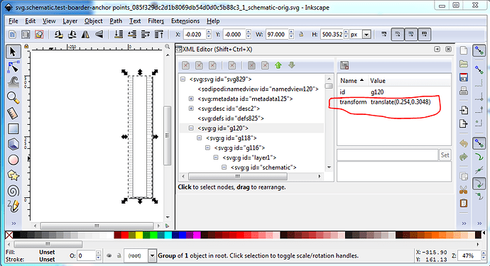
Translates, the source of all evil :slight_smile: ! The work around is simple, fixing the code is likely to be more complex. The issue appears to be a transform in the top level group:

ungroup (to remove the transform)

Now edit select all and group and name it schematic. Then save as plain svg. Rezip it in to a part and load it and now the schematic is correct.

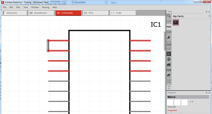
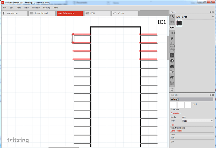
corrected part:

original part:

It appears the transform isn’t being taken in to account when Fritzing adjusts the xml to add the colored line to the connection. With the transform present the new xml gets offset slightly when rendered (likely because the transform wasn’t taken in to account.) so removing the transform makes it work correctly. I expect it may be difficult (unless there is a QT call that will do it!) to apply the transforms (potentially more than one!) to the xml before adding the color markers. This same issue may occur elsewhere if transforms are present as well.

How I would do the schematic for the connectors:

Use the svg.schematic.group-connectors-schematic-template_1_schematic.svg from here

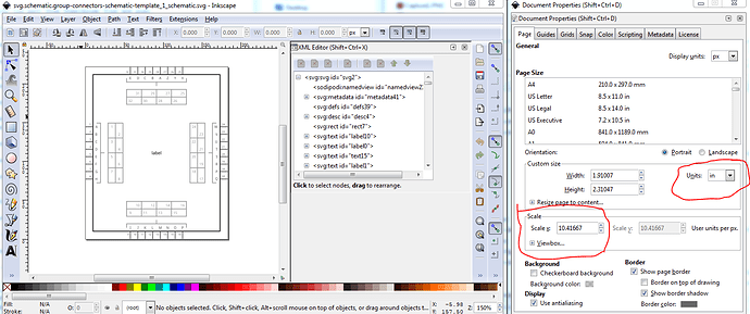
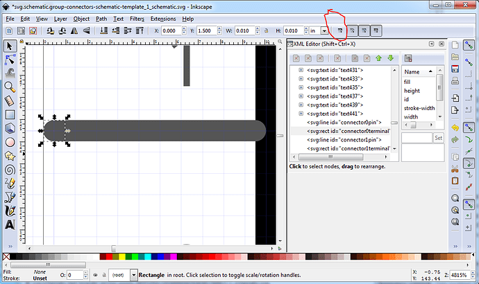
dimensions in in and scale the desirable 10.41667. Pins are .1in long, terminalIds are 10thou 10thou and centered on the end of the pin:

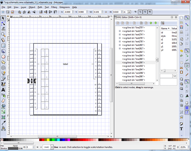
The pin color is #555555 as specified on the graphics standard and the group text and lines are #999999 also as per the graphics standards. I chose to use the group (as opposed to the simple) template because your part has dual row connectors at least in part and the group template will show that in schematic (which I like to do!) Note the template is ungrouped and currently aligned on .1 boundaries so with the tool bar in “in” and the grid size at .1 (or 0.01 in my case) you can move pins around or duplicate them and alignment will remain mostly correct (I tend to check and correct the slight shifts due to floating point roundoff when the svg is finished.) So remove the unused top and bottom connectors (they are in the template so all possible positions are available) to leave a dual row connector on one side and a single row connector on the other.

svg.schematic.new-schematic_1.1_schematic

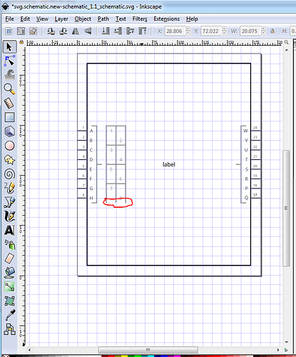
Now delete the bottom most line on the connector so there won’t be two of them after the dup:

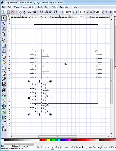
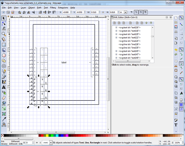
then duplicate the first 8 pins to make a 16pin dual row connector (with some editing):

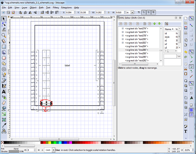
(note this is one position to far down in y, so move it back up 1 via the tool bar like this:

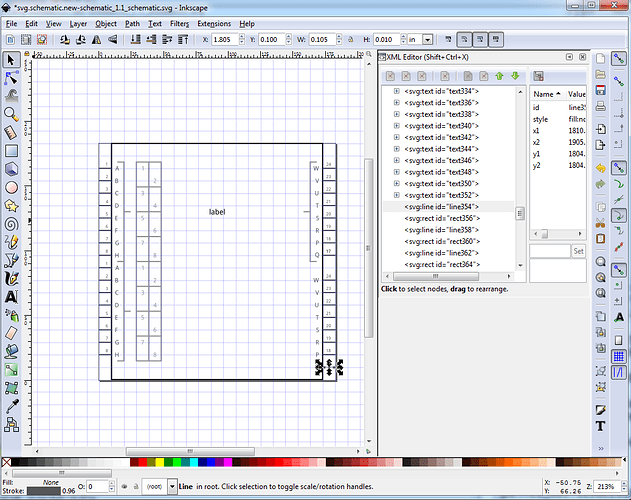
Then dup one of the lines and move it down .1 in via the tool bar to complete the connector and duplicate and move 8 more pins on the right side to make that connector longer.

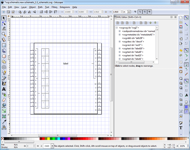
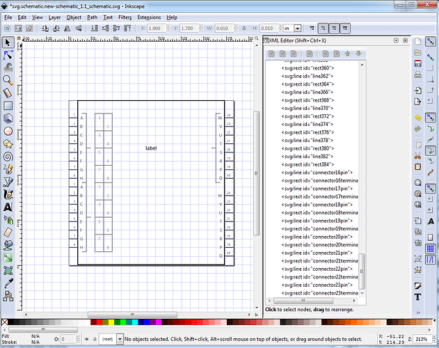
Now move the surrounding rectangle down to be below the last connector, changing the height and width if needed. In this case the height reduces from 2.110 to 1.910. Now do an edit select all and resize page to drawing to correct the viewbox to give the final svg (although the connector numbering is screwed up)

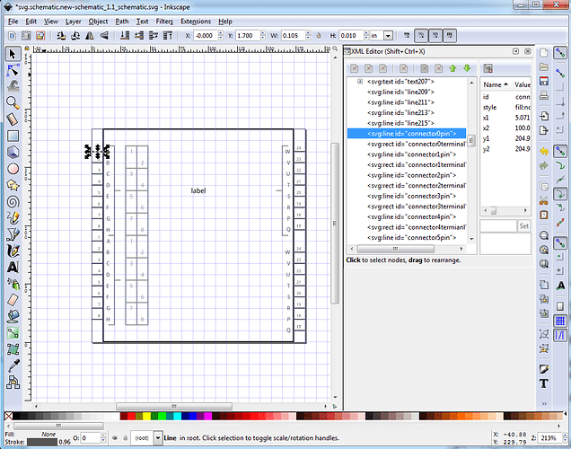
Now to fix up the connectors. To do so start with connector0 and move it (and its associated terminalId to the bottom of the svg via the move to bottom icon on the tool bar. If connector0 wasn’t already labeled connector0pin (it was in this case) you would need to set its id to connector0pin (actually just connector will do.)

There needs to be no labels staring with connector above this as the python script will start making pins (at connector0) at the first connector ID it finds. Now do all the rest of the pins (in the order you want them numbered) the same way. In this case after connector7pin we have an unnumbered (because it was dupped) pin which will become connector8pin and terminal:

In this case I chose to start at the bottom right and increase the pins upwards. You could also choose to use the top right to do the pins in the opposite order.

then proceed to the top leaving you with this:

svg.schematic.new-schematic_1.2_schematic

Now save this as a plain svg and exit Inkscape and run the python script (which isn’t yet public) to renumber the connectors:

$ SvgSetConnectors.py svg.schematic.new-schematic_1.2_schematic.svg

*** Process svg.schematic.new-schematic_1.2_schematic.svg ***
$

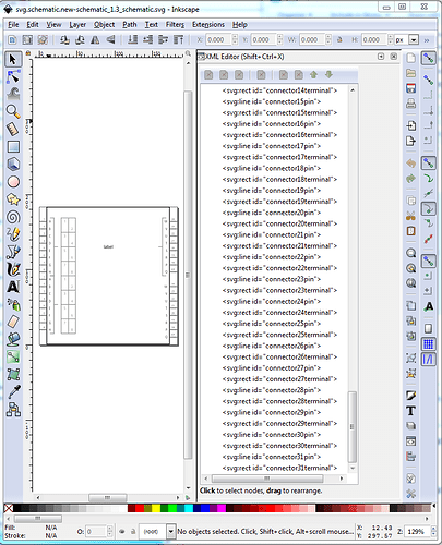
I cheated and renamed the above to svg.schematic.new-schematic_1.3_schematic.svg to have both the original and the renumbered svgs available. The renumbered svg now has the correct connectors set like this and can be grouped (after correcting the text which I was too lazy to do here!) to create the schematic svg.

svg.schematic.new-schematic_1.3_schematic

and schematic is completed. I find this the easiest way to make schematics these days.

Peter

That makes a lot of sense. That transform is outside of (around) the schematic layer/id. Fritzing might only look at the content inside. I thought I could simplify the fix (fudge) process by adding another outer wrapper element (without any transform on it), and moving the schematic label to it. That did not help. So it seems transforms that wrap the complete content cause issues. I have used transforms on blocks of connectors without any problem. It seems the “wraps everything” transform is the problem. I have seen lots of references to transforms causing problems with Fritzing, but this first case I have actually seen it happen. Because my normal process does not ever end up with transforms on those “everything” groups.

The process to fix the image (in Inkscape), is “select all” (which should be the single outer group element: look at the object properties window), then object ungroup multiple times until the selection is no longer a single element. The content of the Object properties window will become ghosted (greyed out) when the resulting (after ungroup) selection is not a single element.

Then group one time, and change the id of the group to “schematic” (in the object properties window). Standard save as plain svg, and good to go.

Using that, then recreating the part, I got the same result as Peter showed in the corrected part screenshot.