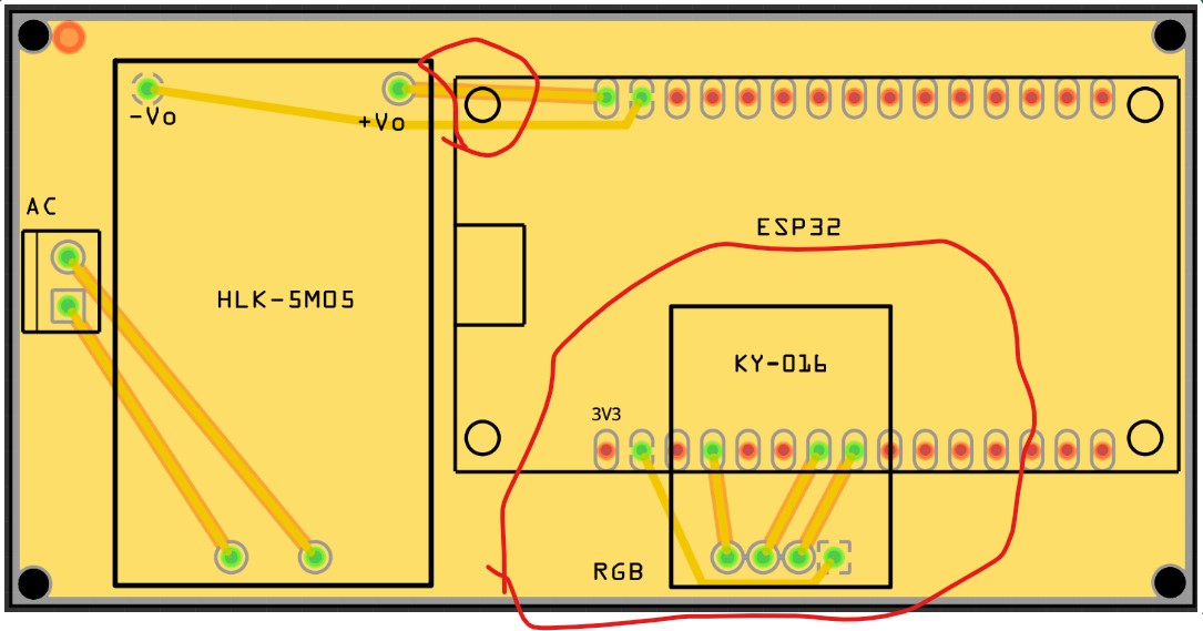
I build a little project to power a DOIT DevKit ESP32 and an RGB led with HLK-5M05.
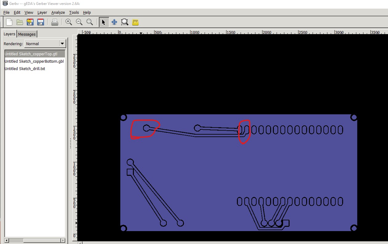
Will this PCB work in theory ? I don’t think the ground appears on my board.
( I draw in red GND who do not appear on the board)
https://imgur.com/a/Tl7bKRM
I build a little project to power a DOIT DevKit ESP32 and an RGB led with HLK-5M05.
Will this PCB work in theory ? I don’t think the ground appears on my board.
( I draw in red GND who do not appear on the board)
https://imgur.com/a/Tl7bKRM
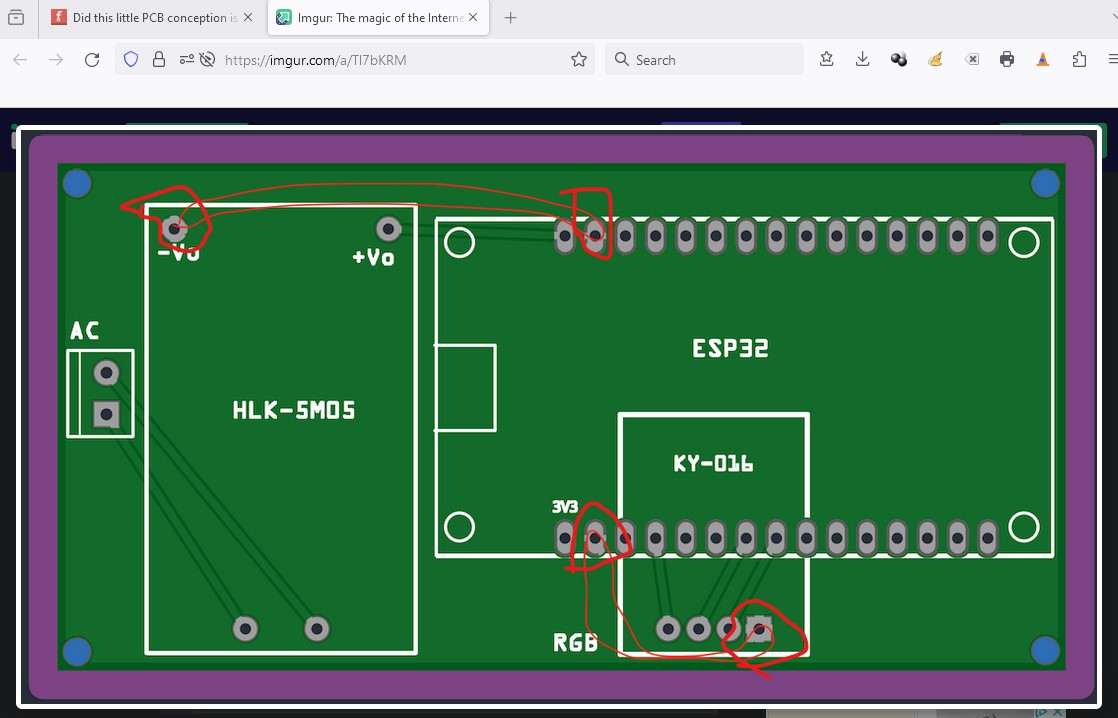
When I did a copper fill rather than a ground fill I saw ground strip on my board.
https://imgur.com/a/4JZUsUT
Two suggestions: 1) you are better to upload the sketch (the .fzz file, upload is 7th icon from the left in the reply menu) so we can look at it in Fritzing from the actual sketch and 2) export the board as gerber files (which is what the board will be made from) and look at them with a gerber viewer to see if the produced board looks correct. Gerber processing happens after the displays in Fritzing and can thus be different from what you see. From your images it looks (although with images it impossible to tell!) that ground fill is correct. In the gerber output (which isn’t here) the ground fill on the top copper layer should show connections to those pads. If it doesn’t you have a problem (and there have been bugs in ground fill before.) Are you running Fritzing 1.0.2 (the latest version which has ground fill fixes?)
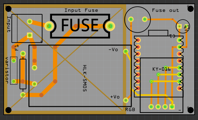
In this copy of your image the parts circled in red are somewhat alarming. The traces are going through the mounting holes and would be cut if you arranged to drill the mounting holes (which you don’t appear to have done. As well the KY016 overlaps the ESP32. The will work if the KY16 is on the bottom of the board and the ESP is on the top but otherwise the two will overlap and likely not work physically.
Here I have circled in red the apparent ground fill pads, the small squares on the sides of the pads appear to connect to the ground fill correctly assuming the green is the ground fill, but I can’t tell from an image. As noted the gerber copper top output would be the place to verify that.
edit forgot to upload the 2nd image!
Peter
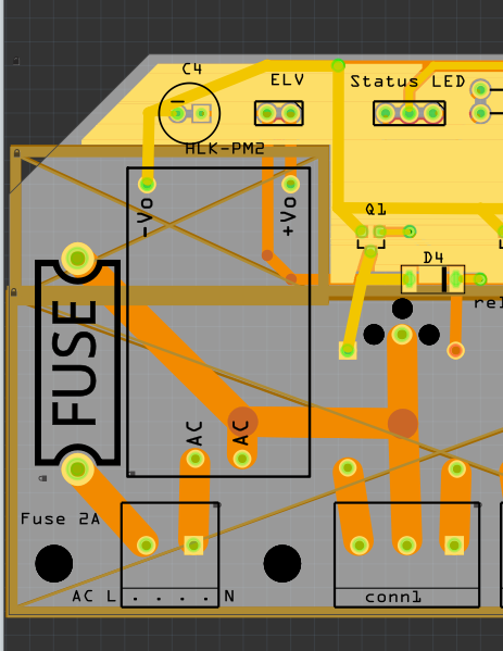
Your AC is 240V or thereabout. For safety reasons you should consider sufficient distance and certainly have no (shared) copper fill with the ELV side of the circuitry.
If it were my board I would route the tracks at a safe distance in an area with no copper fill top and bottom.
Note that there is a (touch protected) fuse for some protection against faults.
Also note that the area with 240V tracks has been spared from copper fill.
Tracks have been kept at a distance and a larger track size had been used to not make the tracks becoming the fuse.
Whilst there is room for improvement on this example too, I would under no circumstance embed the 240V tracks in a shared copper fill. Anything going wrong has a high risk to turn your PCB into a hazard.
Your 240V tracks also are at almost touching distance, this might not end very well.
I route all 240V tracks on the bottom layer only and avoid anything unprotected on the top layer if I can. In case something like a Varistor is needed, this can be embedded in some shrink hose for touch protection and to avoid it blowing all over in case of catastrophic failure.
Hello Peter
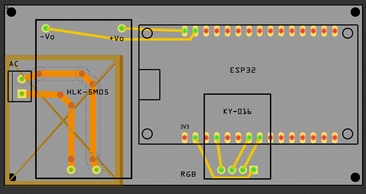
Thank you for your reply. Here is the sintering project.
Project.fzz (84.1 KB)
I can’t attach the Geber files in the post but they are extracts from the Fritzing project.
In fact, I’m using the latest version of Fritzing.
On the ESP32, the mounting points will be drawn and not drilled.
The KY-016 is positioned vertically so the display on the board is wrong, they won’t overlap.
I understand that the green layer is the ground so logically my HKL should received all the ground on “-V0”.
Hello bombinho
Thanks for your advice, I’m going to try a new version to separate the 240V circuit from the ELV circuit.
Do you have an example of a Fritzing project to understand how to do this?
Regards
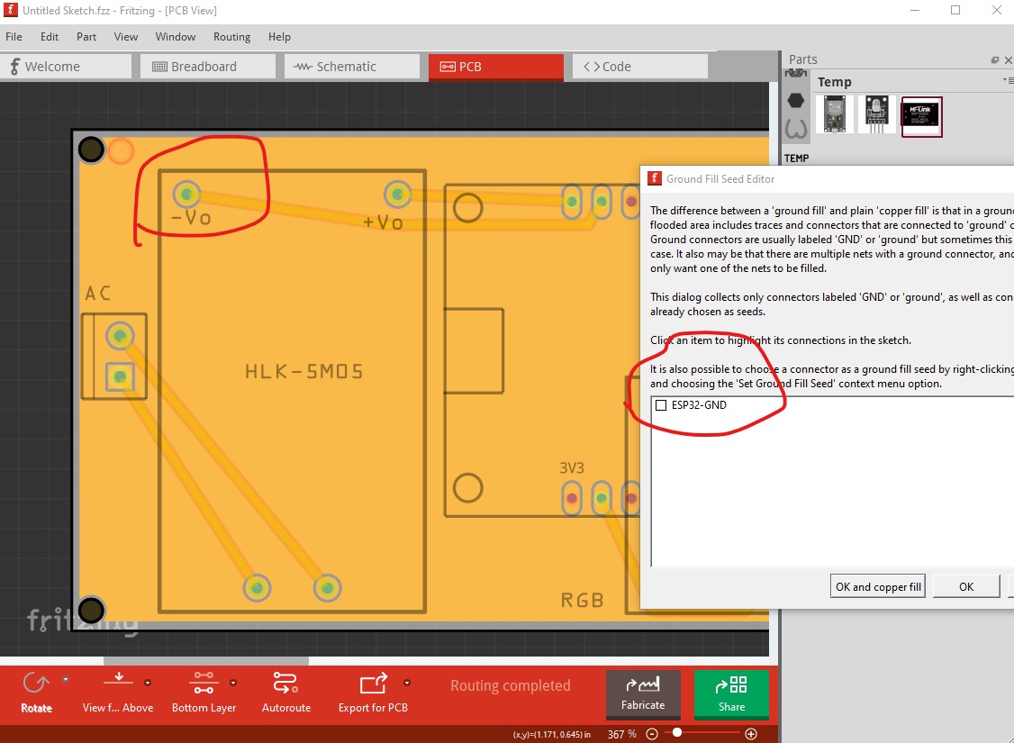
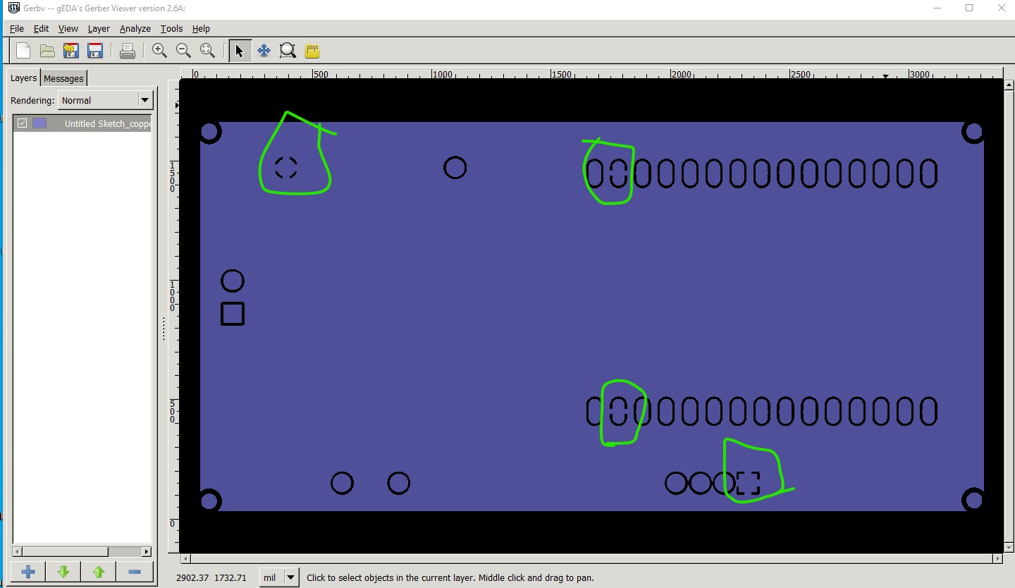
It appears you haven’t set the ground fill seed and thus ground fill hasn’t worked correctly. This is routing->ground fill->choose ground fill seed which sets what net will be ground filled. It currently has no selection so doesn’t ground fill any net shown by the lack of a connection to the ground fill here
which translates to the gerber output (displayed here in gerbv.) The ground connection is a trace and doesn’t connect to the ground fill.
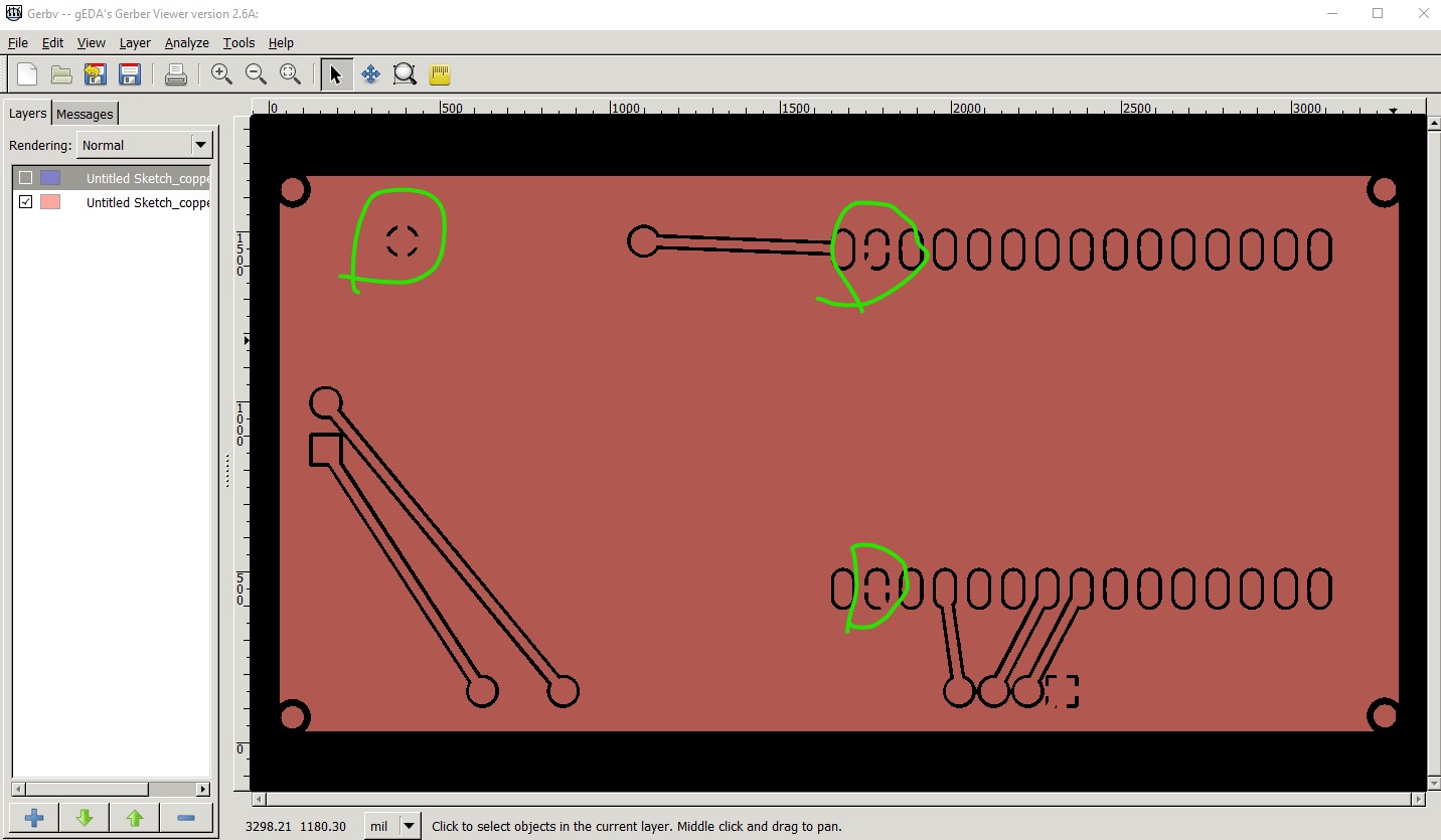
setting the ground fill seed and clicking ground fill top and bottom in the ground fill menu establishes the ground fills correctly on top an bottom layers.
Peter
I only have looked at the AC side and not implemented Peter’s suggestions, I also have removed the copper fill for now.
This is a crude example, not including any fuse (holder), which I consider advisable.
The tracks are enlarged to 60 ([Width], manually enter a figure if you do not want to use the pre-set sizes, in this case I typed 60)
The tracks are moved to the bottom layer. You can do this easy by right clicking the track and clicking [Move to bottom layer]. Also you can do the same thing by selecting the track and change [PCB layer] to ‘bottom’.
The track distance has been enlarged by using bend points and moving it slightly.
Copper fill blocker has been located top and bottom. I have locked the PCB in place as well as the bottom copper blocker. I left the top at a slightly different size, so it is easier to see and I have not locked the top copper blocker.
Untitled Sketch_CopperBlocker.fzz (66.8 KB)
Thanks for your help!
I’ll download and look at your modifications.
I’ll look at how to add a fuse (I’m currently searching for the component on the web).
A google search of the form “fritzing part fuse” turns up a variety of hits.
Peter
Thank you Peter for your explanation. I understand what you mean.
I will try with a fuse and post here the result of the fritzing to get your opinion on the result if you agree.
What do you think about this type of hardware conception ?
Can I adapt this breadboard to mine?
It should work but it has screw terminals and no mounting holes that I can see to mount it to the pcb (and I don’t know of a Fritzing part for it.) So you would probably want to mount it off board and run wires from the 5V output to your board. It looks to have all the desired protectopn built in.
Peter
I came back with a new version.
I’m not sure at all if it’s better.
I tried to separate in two board to minimize 2D space with a mounting.
Project_v2.fzz (84.8 KB)
PS: I dont know which capcitor ref I should take.
While it should work as it stands, I made a few improvements (which you may or may not agree with!)
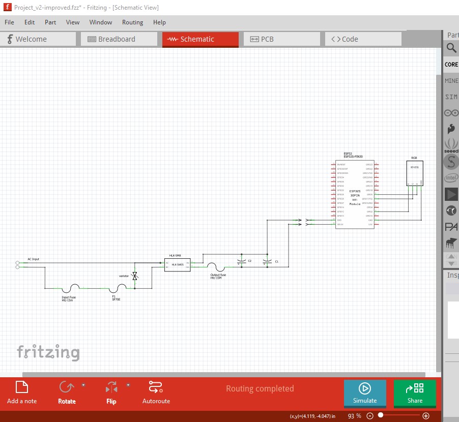
I replaced to DC screw terminals with a 0.1in header (male on the power supply board, female on the CPU board) which will then plug together. I moved all traces to the bottom layer and rerouted some of them to take 45 degree bends (which is recommended best practice on pcbs.) I removed the ground fill blocks as it was effecting schematic (which appears to be a bug which I will report!) and you don’t appear to be using (or need) ground fill. The KC-016 overlapping doesn’t matter because the part silk screen is wrong the actual device has right angle connectors and stands vertical. I added holes for the 4 mounting holes on the esp board so you can screw it down if desired. You need to make sure the two headers are at the same x-y position on both boards, I think that is likely true now but checking it would be wise before ordering boards. I also populated schematic as a check of the circuti. It is very easy to make a mistake in pcb, but if you populate schematic after routing pcb and schematic looks correct then likely the board is correct.
the changes are contained in this sketch
Project_v2-improved.fzz (87.6 KB)
Peter
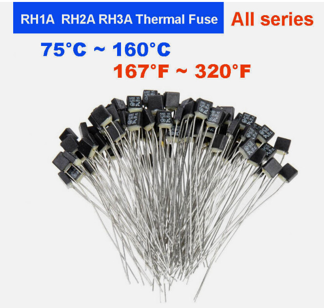
The level of protection of the circuitry is quite comprehensive. What I personally don’t like is bare life wires on a board (It might be me, who has to work near the board again, also tight casings are prone to have things touching that should not). There are thermal fuses available with bottom entry like these:
Note that your thermal fuse should at least be able to carry the current that your fuse is rated for.
Fuses are available in many shapes or forms. I like the fuse holder you have used for its easy availability and low cost of the holder and the 5x20 fuses.
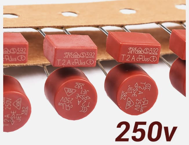
Other more space saving options, whilst remaining touch safe, are available too. Like these (TE5, TR5):
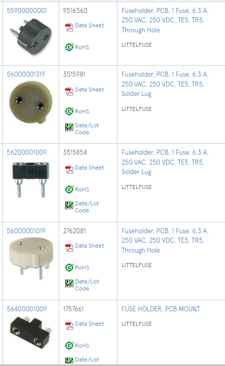
Even fuse holders exist for them
Also, your Varistor is prone to fail catastrophically at the end of its life, after a history of overheating. Placing it very close to a thermal fuse can prevent nasty surprises.
The Varistor is there to catch voltage spikes. The most typical occurrence of such spikes are switched AC loads. Whilst you might get away without one in a simple power supply + ESP, it makes sense to have it in place once equipment starts switching things.
If you want to squeeze it all onto one board, you could consider using a much smaller version of the ESP32 like this one:
These are very competitively priced and I have started using them instead of the D1 mini, which is available as ESP8266 and pin compatible as ESP32 too (with a slightly larger board size).
I have used different pins though.
Note the use of a screw terminal with 5.08mm pin spacing. The 3mm are a little small for 240V IMHO.
I already have the ESP32 so I design the board with this model.
@vanepp @real-bombinho thank you for all your response.
I will work on the board today and the list of the hardware I have to command in the post for posterity.
I normally try to have the materials already available when finalising the project as it has proven a good idea to print out the board and poke holes where the through holes are and then place all components on the paper print-out to ensure they fit.
Only then I go and order the board.
You may find that your boards cost you as much or more than the components on simpler boards.
The main thing is that you enjoy it and have something that does what you want.
And remember, do not do anything with 240V (LV) when you are not sure what you are doing, as you and others can get hurt.