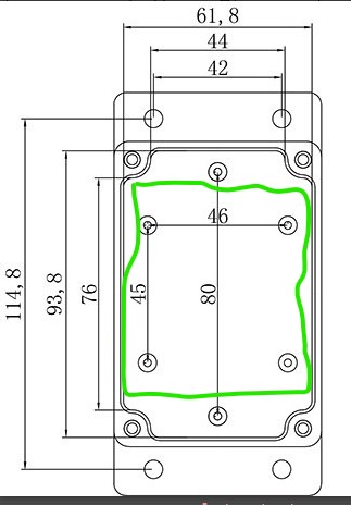
My wish. It is a bit tough for me to learn a vector graphic program. So, It will be easier for me if Fritzing has a custom PCB shapes for a popular box selling on Aliexpress.
I have a few boxes in my mind such as:
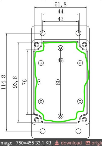
My wish. It is a bit tough for me to learn a vector graphic program. So, It will be easier for me if Fritzing has a custom PCB shapes for a popular box selling on Aliexpress.
I have a few boxes in my mind such as:
You would need to specify the shape you want for the board. There are several possible. From easiest to most difficult:
easiest (just change the size of the default pcb in Inspector to make the rectangle bigger)

more difficult (but I expect what you want) which requires a custom board shape.

but provides maximum layout area. Or something in between which would still require a custom board shape.
edit: as well there is the rounded rectangle and other custom board shapes which may do what you want
again you can change its size in inspector to the size you want.
Peter
I can offer you an Eagle .brd file (Enclosure 100x68 PCB Outline.fzpz (31.7 KB)—this is actually a .zip file, I had to add the .fzpz extension to be able to upload it, so you may need to change the extension to .zip before dearchiving) that contains the requisite shape in the Dimension layer.
You might then be able to use something like the Eagle-to-Fritzing tool to convert that to something that you could use in Fritzing.
I do note, however, that this ‘outline’ includes slots to accommodate the slightly different locations of the mounting points in several different enclosures of the same external dimensions that I have encountered. If they are a problem, I can easily remove them.
If you can make this work, I also have other [Eagle] PCB outlines for a couple of other common [AliExpress] enclosures.
I can see the brd file in Eagle but the first run through with e2f didn’t work correctly which may be an issue on my part. I’ll poke at it some more and see if I can recover a pcb svg file from it. It may be a no components issue as I don’t think I have ever converted a bare outline without any parts. We will see and go from there Thanks for the .brd file!
Peter
OK, I got a svg that I think is like your path. I haven’t yet managed to difference the paths successfully but if you can check this svg against a board and tell me if the holes are accurate that will help:
(right click on the image and save image as will download it)
Peter
I’m not sure if the scaling is correct. Just printing out that SVG (from Affinity Designer or Inkscape) yields an outline that is ~67.5mm x 42mm—the dimensions of the outline within Eagle are 88.9mm x 56.9mm (actually 3500mil x 2240mil).
If it helps, the file I originally sent had an additional bounding box in the Dimension layer that should have been in one of the Doc layers. The following (again renamed from .zip to .fzpz for upload) simply contains the board outline (and holes/slots), in the Dimension layer, as originally intended.
Enclosure 100x68 PCB Outline Only.fzpz (31.6 KB)
I notice that one of the Gerber files generated from that board file is top.svg, which would appear to simply be an SVG file of the outline, if that helps. This file displays as I would expect within Affinity Designer, but Inkscape seems to lose the holes…
OK, I’ll scale the svg up to match that. I don’t much use Eagle other than for e2f so I’m not clear on how to get measurements out of it. I don’t think eagle2fritzing processes the document layer only likely copper1 copper0 and silkscreen. It in any case doesn’t produce any useful output so I took a screen show from eagle and imported it in to Inkscape and though I had measured the width as 67mm but may have gotten that wrong. I’ll scale it up and see what happens. OK scaled up it is 88.9mm wide by 56.448 wide which should be close enough I hope. Here is a new svg.
if you could try this one. As always the svg difference conversion in Inkscape is screwing me around. In theory the first path should have been cw but appears to be ccw so I’m currently trying to convert it to CW and then hopefully the rest will fall in to line (as I am converting the holes to ccw) and the difference operation will give me slots. The board has to be custom loaded anyway so the slots aren’t a problem (other than generating them correctly which is always a pain!) Hopefully the holes scaled up correctly, if not they are easy to move.
Peter
Yes, that’s now a pretty good match. Note that the only reason that the outline includes slots is to cater for slightly different enclosures, which share the same basic dimensions but which come from different suppliers and vary slightly in style and the location of mounting posts. If the user is always using the same enclosure supplier, correctly located holes are all that would be necessary.
Assuming I can get the damn svg to work slots are easy enough and the most flexible so I will go with that. Thanks for checking!
edit:
I’ll be damned, for once editing the svg to be correct worked.
This svg when loaded in to Fritzing should cut the appropriate slots
edit2:
replace the svg with one with a stroke-width of 1 which outlines the holes. Don’t route traces over the holes as they will be lost when the holes are cut!
edit3:
replaced the svg with an improved version which shows the extent of the holes.
the slots are now visible here and they are there in the gerber output in contour.gml:
@somsak To use this you need to right click on the board above then select save image as to download the file outline.svg. Once that is done start Fritizng switch to pcb view and select load image file.
at the prompt give it the outline.svg file you downloaded and click OK
edit3:
replaced the image with an updated one.
this is your board with the slots (although they aren’t visible which is a pain as you need to avoid the holes with traces, I’ll poke at that and see if I can correct it!) Now you set your circuit up as normal and when you export the board to gerber the slots will be cut as you see in the gerbv output above.
edit2:
Reuploaded the svg file with a fixed one that shows the holes.
edit3:
reloaded the svg file yet again with a better silkscreen that shows the holes. In a bit I will upload a part that includes this outline which will avoid needing to load the image file in to pcb view (as well as documenting how to do that.) Then you can load the part as normal and the custom pcb will be present ready for use. If there are more sizes you would like it should be relatively easy to create them from the first outline svg.
Peter
OK so I figured out and documented how to create this as a part
This part
aliexpress-box-outline-100mmx68mm.fzpz (2.4 KB)
which looks like this in Fritzing (note I deleted the pcb rectangle that loads by default because if you don’t you have to select which board you are referring to and you can only drag the part in to pcb view not breadboard or schematic which it doesn’t have!)
and exports gerbers like this with the slots cut.
and the contour.gm1 file which actually cuts the slots and the board edges
Peter
OK, here are two more for you, PCB outlines for 85 x 58 and 63 x 58 enclosures:
OK try these two I think they should do the job.
edit
replaced both with improved versions, the 85x58 has the most changes but both should now be correct. Same moduleId so you will have to delete the old ones then shutdown Fritzing (to really delete them) before you will be able to load the new ones.
aliexpress-box-outline-63mmx58mm.fzpz (3.3 KB)
aliexpress-box-outline-85mmx58mm.fzpz (3.3 KB)
as before they are parts so can be just loaded.
Peter
There are some extra lines there on those parts, probably most obvious on the 63 x 58 one:
I loaded aliexpress-box-outline-85mmx58mm.fzpz in Fritzing. Put a few part and try to export as gerber files.
When I exported, I saw a few error messages. Copper0 layer export is empty, Mash0 is empty, paste mask layer is empty.
The mask error messages are normal. This appears to be only an SMD board so it only has copper1. The gerber output doesn’t appear to be normal though, but from a picture I can’t tell anything. You need to upload the sketch (the .fzz file, upload is 7th icon from the left in the reply menu) so I can try your sketch to see what is going wrong. This is a test board done on Fritzing 1.0.4 on Win10:
First you need to remove the original pcb part (which it looks like you have done) leaving only the new part
then I added a couple of SMD components and created a couple of traces and exported as gerbers. The error messages appear and I click OK.
which correctly exports the sketch as a gerber file (here displayed by gerbv)
If you upload your sketch I will have a look at it. What Fritzing version you are using would also be useful as this feature is relatively new.
Peter
mySketch 2.fzz (6.8 KB)
Error may be because I use an old version fritzing.0.9.3b.64.
I view gerber with ZofzPCB.
Yep it likely is. 9.3B has a variety of gerber errors that were corrected in later versions (plus the part type forms were not supported that long ago.) Turns out I am partially wrong 0.9.3b will accept the part but doesn’t render it correctly. Your best bet would be to upgrade to 1.0.4. I could possibly adjust the svg to work on 0.9.3b but it likely isn’t worth the effort and may not be possible. This is the gerber output from Fritzing 0.9.3.b with the part which renders incorrectly (likely due to known gerber bugs which have been fixed.)
as you see the outline doesn’t render correctly.
Peter