Just printing it should do the job. The printer driver should make the output 1:1 scale. To check print out something known like a 16pin IC and check that against a real part, if that is correct the custom output should be as well.
Peter
Just printing it should do the job. The printer driver should make the output 1:1 scale. To check print out something known like a 16pin IC and check that against a real part, if that is correct the custom output should be as well.
Peter
I printed one time but PCB is smaller than expected. I will try again tomorrow.
As I said, I would try with a known standard part like a 16 pin DIP IC (which should be 0.1in between pads and thus 0.7in start pad to end pad)
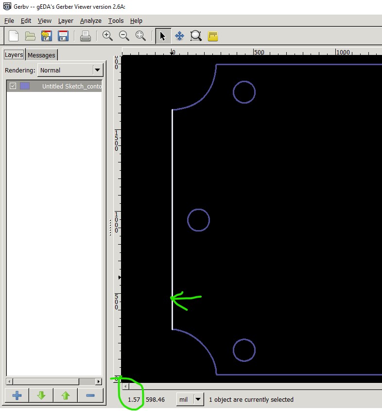
or easier yet just put a 16 pin DIP IC on top of it and see if the holes are correct. If they aren’t you need to do something with your machine’s printer driver to get it to print at 1:1 scale. Measuring the length of the custom cutout should also work to see if it is too short. Here I exported the sketch as gerbers then used gerbv to display the gerber and selected the start position
1.57mils (1/1000 of an inch)
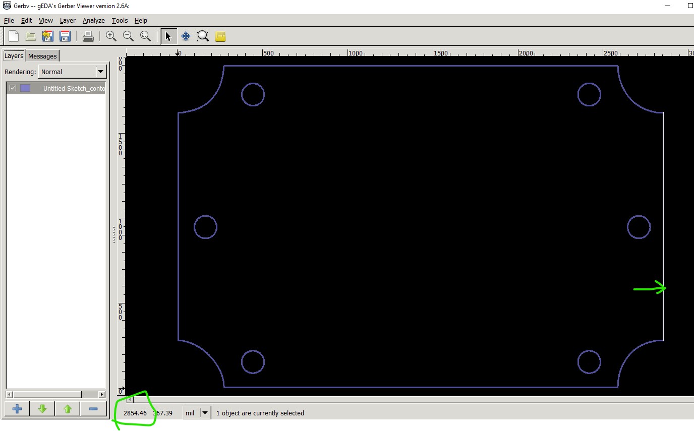
then the opposite edge
2854mils or 7.2cm
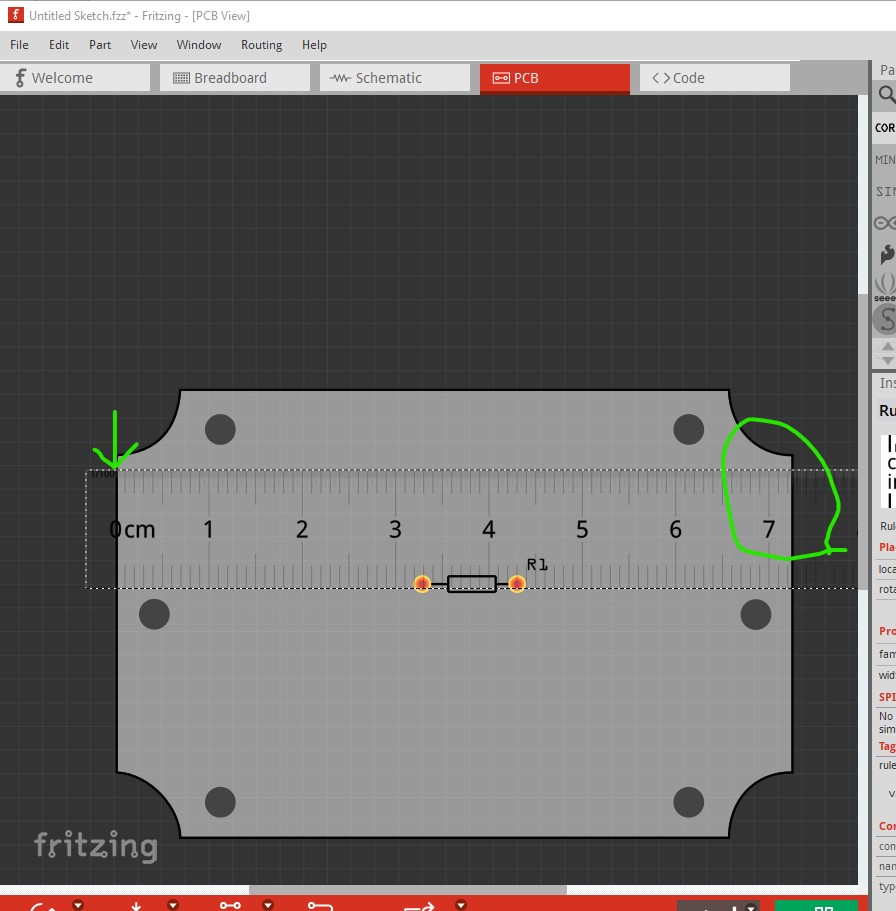
which is around correct according to the ruler in Fritzing.
The gerber output is what the board will be produced from, so so long as it looks correct the board should be fine.
Peter
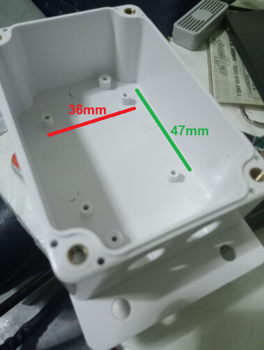
The internal width should not be 7.2, it have to be 9.38 on my first post.
About printing, I can now printing exactly the real size with my Laser or my Inkjet.
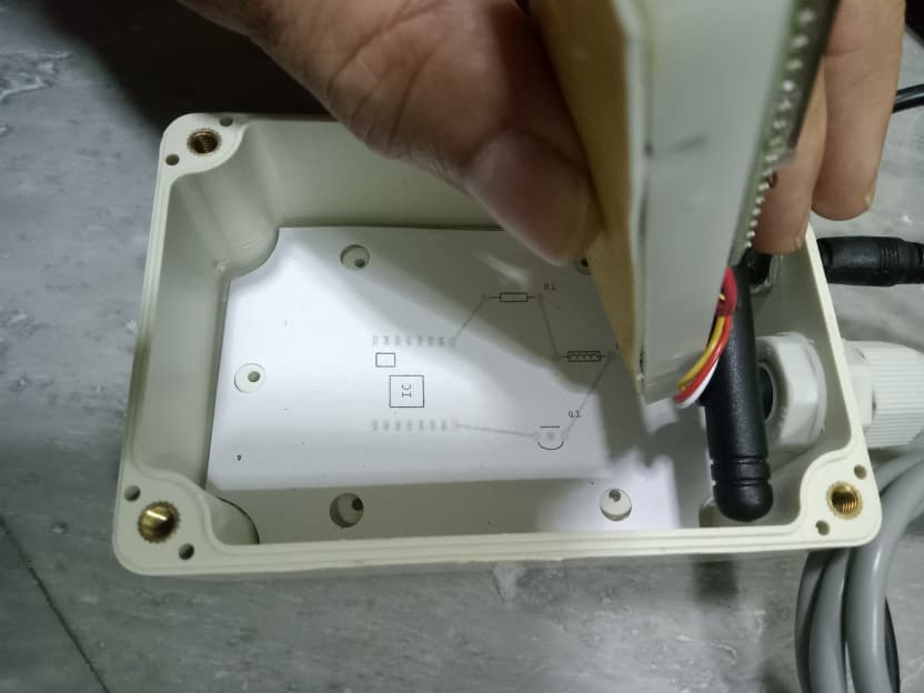
Anyway I found new problem with the box. It is not consistant in internal holes even though the other sizes are looking the same. You can see my new box is not the same as I gave the dimension on the first post.
Thank anyway, It seems my idea to prepare custom PCB is not applicable at the moment.
I would not say that. The boxes so far produced match the boxes @UniquePete uses. If you need a different shape it is relatively easy to make one by changing the svg and creating a new part. So try this part (which was created from your original post’s jpeg image.)
aliexpress-box-outline-115mmx68mm.fzpz (2.5 KB)
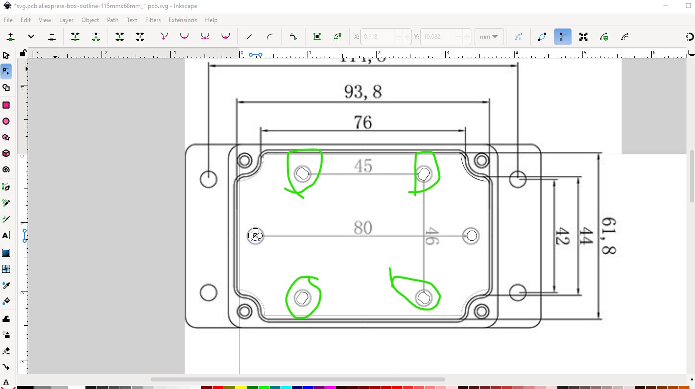
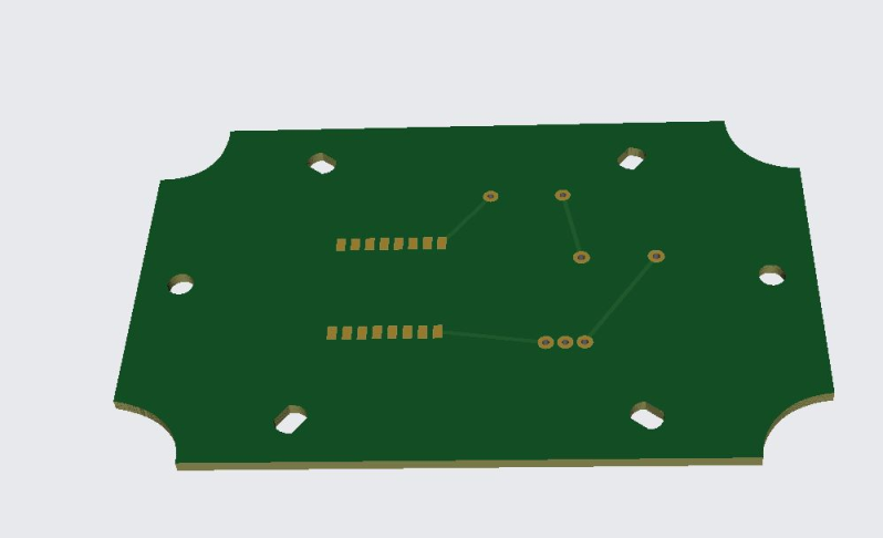
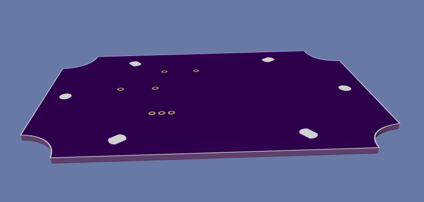
and looks like this (note the outline may be too close to the edge of the box and require adjustment as it was made from a jpeg image which isn’t the most accurate outline!) Note the 4 holes (which are slots) circled in green. They can be turned in to holes if you wish. In the original they are designed to fit multiple different boxes. This is the svg with the jpeg image of your board overlaid on it.
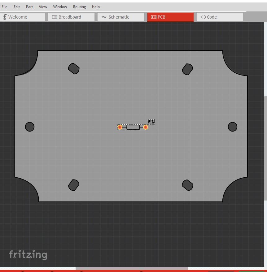
which produces this
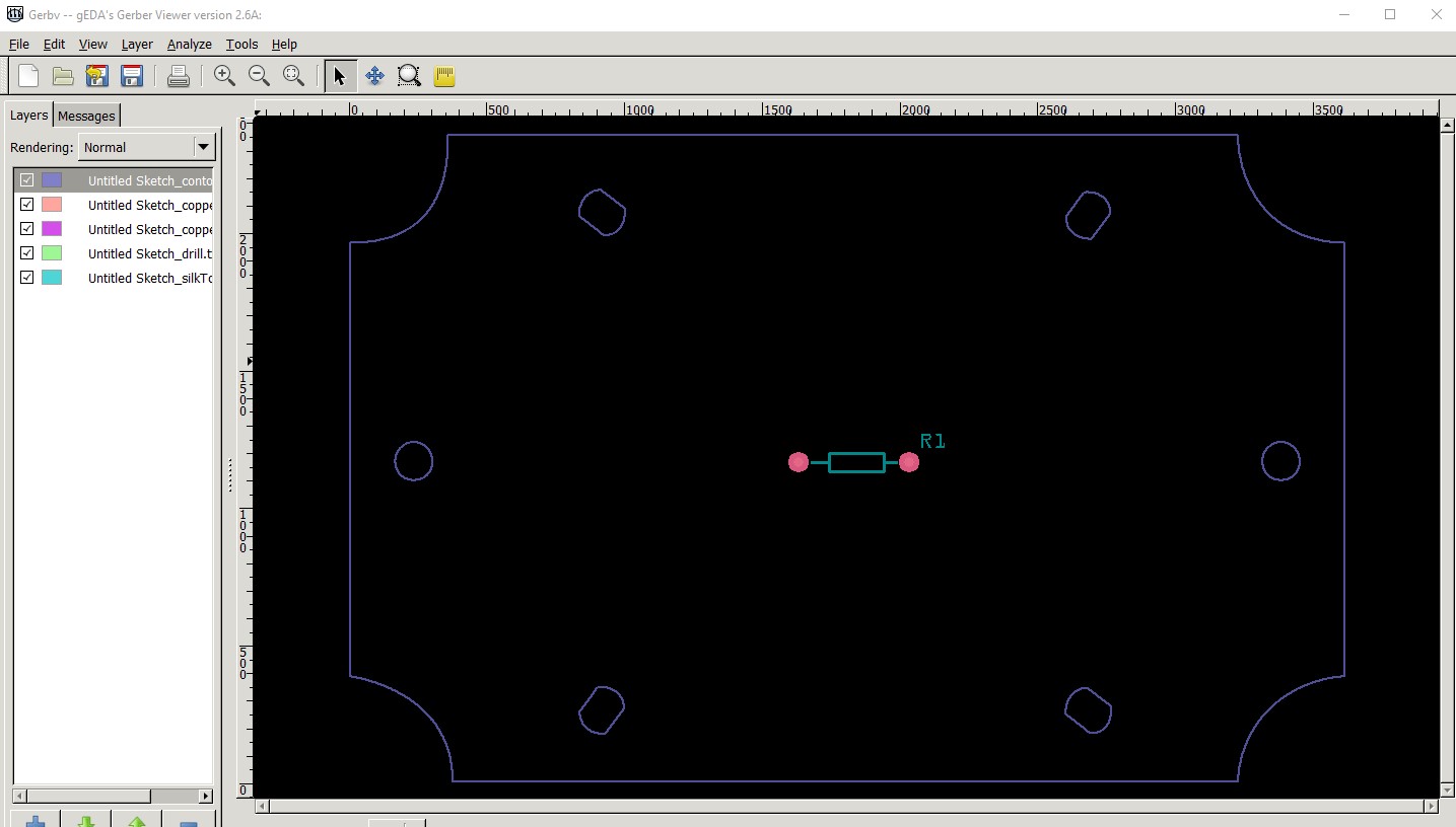
and these gerbers
for small numbers I don’t mind doing the necessary changes, if you want lots of different boxes you would need to learn to do the modification for yourself (which are not particularly easy if you aren’t familiar with Inkscape.) I don’t mind demonstrating how I did this in an example to help you learn how to do it.
Peter
I tested aliexpress-box-outline-115mmx68mm.fzpz (2.5 KB)
It fits to my old box very well.
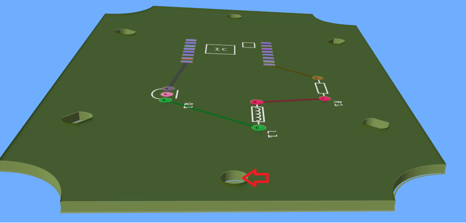
I previewed with JLCPCB, 4 Green Spots are looked like real holes.
Should be, although only a board will say for sure. The gerber output indicates they are slots and holes and thus should appear on the board. The last image above appears to be showing the 6 holes as holes (they have white which should be the holes.) That said I don’t know ZofzPCB viewer so I can’t say for sure what it does. Why do you think they aren’t holes there?
Peter