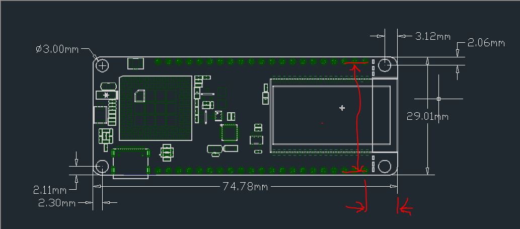
Easy enough to do, but I need some more information. The mechanical drawing has most of the needed dimensions, what is missing (and required) is the positioning of the header connectors from the end of the board and their spacing (it looks like 1.0 in as the board is 1.1in wide.) If you have a board and can provide the measurements I can make a part (if you like it, feel free to donate what you think it is worth on the Fritzing donation page to fund development)
the shaky lines in red indicate the required measurements, preferably with vernier calipers, but a ruler will also probably be close enough (the spacing can be adjusted once the part is made to match a real board.)
Hi.
I have the a PSD (Photoshop) file with all you need to get the measurements. Or I can just upload it to this post as a jpg like the one you have. Please advice.
It looks like infinview wil read either so either should be fine.
Yes (although I had to poke to remember how ), click on your icon on the top right then click on the middle icon of the three that come up on the bottom of that window and you are in the messages interface and new message should do it.
edit:
OK here is a functional (but probably not correctly aligned) part. When I get the connector positions I’ll correct it (and maybe improve breadboard some)
edit: Corrected somewhat the pin spacing, still needs work though.
The battery terminals are not in the part as they are on the bottom of the board (and don’t appear to have a + and - set) there are also a number of typos in the pin listing (such as GPIO33 where it should be GPIO26) which were corrected.
Hi Peter.
Thank you so much for your help.
I feel a bit stupid because I can not find the donate button or how to.
Please let me know so I can contribute.
You are much faster than me. I will send you the psd when I wake up. I live in Norway it may be some time difference.
I’m looking forward to test the part. This is so cool !
Thanks !
Don’t feel bad, I can’t immediately find the donate button either (it is on the main web site somewhere, although that is running slowly right now). The download button on the main web site does have a donate button, but I think there is another one somewhere too. I’m on the west coast of Canada so there is probably a fair bit of time difference.
OK, I converted the .psd to a jpg (which Inkscape will import unlike the psd) and imported it in to the Inkscape breadboard view. Unfortunately when I scaled it so the headers are correct (they are on exactly .1in boundaries) the mounting holes in the .psd are slightly shorter in Y than the measurements in the dimension drawing posted above. I split the difference between the two sets of mounting holes, but the position likely isn’t exactly correct yet. The easiest way to fix that is for you to print out the pcb view at 1:1 scale (preferably on an clear overhead transparency) and compare it to the real board. The header holes should all match exactly, but the mounting holes may be off by a bit. If you can measure how far off the mounting holes are in x and y for each hole I can move them in pcb to match the real position. I have replaced the part posted above with the corrected part. Note as usual, the mounting holes are only on silkscreen in the part, if you want holes on a board you make, in the sketch you need to drag a hole from the pcb area of core parts in to the sketch and set its diameter to 3mm and place it over the hole in silkscreen so the hole will be drilled in the board (if you don’t want the mounting holes leave it as is.)
Finally found it if you start Fritzing and click Help->Donate to Fritzing it will take you to the donations page. I thought there was a link on the main web page but don’t see it there.
He he. Ok. I really think that Frizing is a good initiative and I think it would be smart to bring the donate button on to the Main page or at least somewhere in the forum. I will go ahead and donate.
I have easily created my first PCB and I have sent the order to AISLER.
I think it used to be there, and probably will be again. At present however the web site is fragile. There is no staging environment, it has had no (or at least very little) maintenance for 4 years and changes have to be done on the live web page. I see it has been upgraded to use https recently (it used to be http) and likely the passwords all reset (I had to reset mine anyway!) so work is being done in the background as time and funding permit. Doing more is what trying to improve the donation rate from the current less that .1% of downloaders is about. The code is too complex to expect volunteer help, judging from the lack of any help in the last 3 or 4 years, so funding professional developers looks to be the only way forward. Hopefully the email alerts for replies like this one will start working again too. After I hit the reset password button, I realized if replies from Fritzing were being classified as spam and being discarded I was in trouble, but luckily the reset email did indeed come through, indicating the problem with no email alert to replies is with the forum not spam discard and hopefully will get fixed.
Hopefully you printed out the new pcb footprint and compared it to a real part, because if it is wrong (which it may be) the board will be too …
You are most welcome. Keeping people interested in using Fritzing is the only way it is going to survive going forward.
Right now they are having problems even upgrading the web site. It has had little maintenance in the last few years and is very out of date and thus fragile. The recent login problems are being worked on and hopefully will be resolved soon (they may be now, I was able to log in first time when I tried this time without the “there is a problem with your account” error so far, although that may just be chance.) There is a lot that needs to be done and donations help getting that done. Indeed a merry christmas to all!
Note: the vias for the thermal pad are only on silkscreen (because it is more difficult to make a mixed smd and through hole part) so you need to drag a via from core parts over top of the silkscreen markers in your sketch to get the proper vias. Also as always print out a copy of the pcb image at 1:1 scale and check it with a real part to make sure the footprint is correct before ordering boards. If you actually want a breakout board, we would need a pointer to the board preferably with a mechanical drawing.
Hello. Thanks for the .fzpz file. I want to mount my board with the SIM card facing up. Do I need a different file for this? or is there a way to flip ( not rotate) in the Fritzing app?
Thanks for a great forum
On the PCB view, it should be enough to move the part to the bottom layer. After it has been initially placed, select the part, then in the Inspector window, placement section, change “pcb layer” to “bottom”.
If the part is directly dragged from a bin to the PCB view, it will (with the current Fritzing version) be placed on the bottom layer if the view is set to “Bottom Layer” for the clickable layer(s) selection with the toolbar at the bottom.
Make an enhancement request on the github issues page. I expect this will be a lot of work and there are much more important bug fixes to do first though.