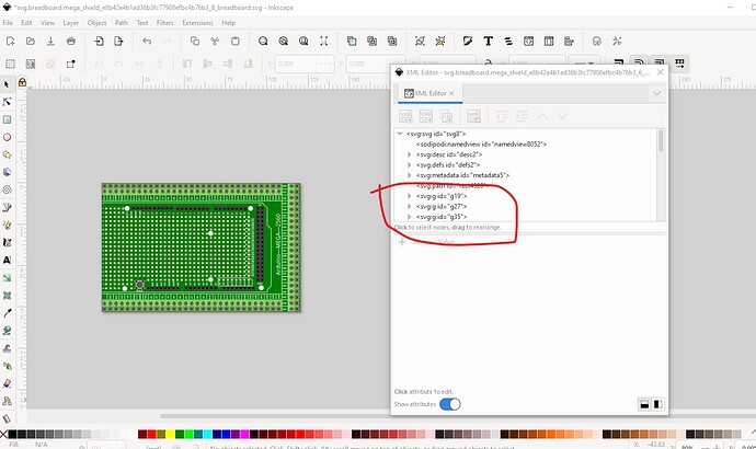
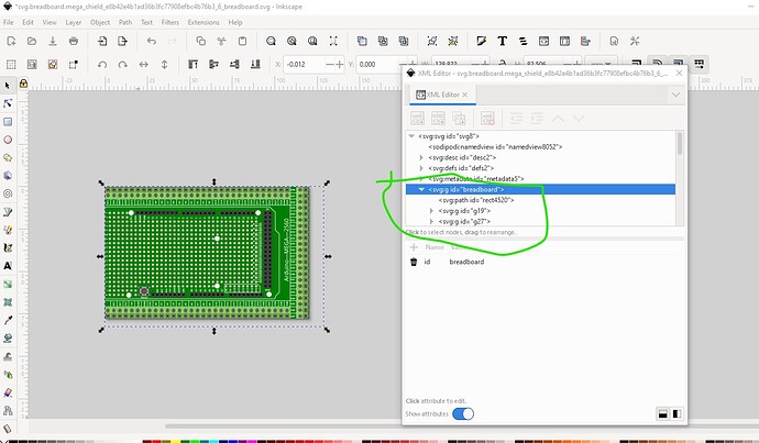
OK finally done. This has been a really worthwhile project (if time consuming  ), while testing the final board I have managed (I think, more examination is required!) to reproduce a bug that causes routing database corruption that I have been chasing for the last 5 years. First time I have managed it and it tells me what to do to cause it maybe. In any case on to your board. Starting with the breadboard svg, here is the cause of the missing layerId message from FritzingCheckPart.py
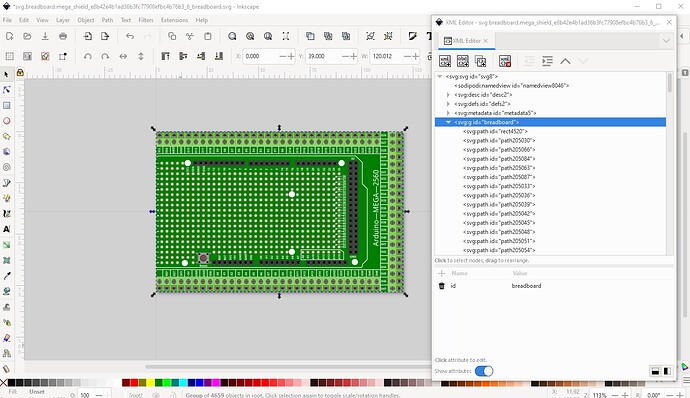
there needs to be a group (typically called breadboard, but perhaps breadboardbreadboard if you cloned a Mega part) that contains all the drawing elements like this
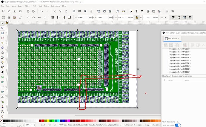
An Edit->select all indicates there is something not easily select able outside the board boundary
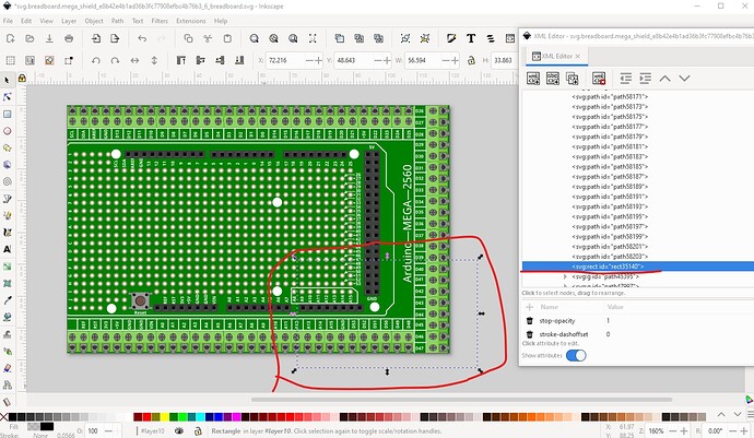
It appears to be an unused not rendered rectangle that I will remove.
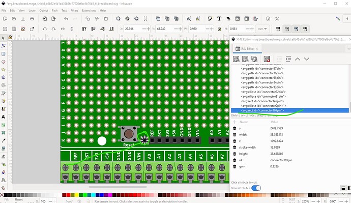
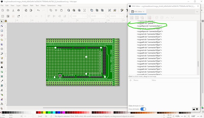
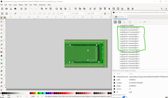
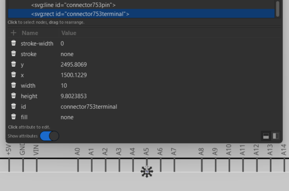
Then starting from the bottom left move the connectors to the bottom of the svg (to facilitate renumbering) like this.Note this is going to be somewhat strange bacause I am looking ahead to what I want to do in schematic so the order is not all that intuitive but I will explain.
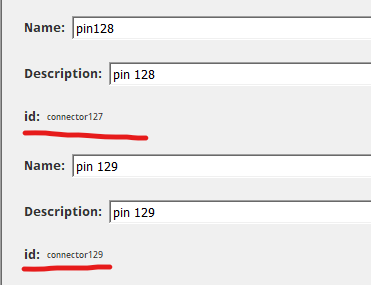
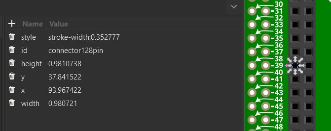
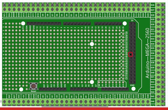
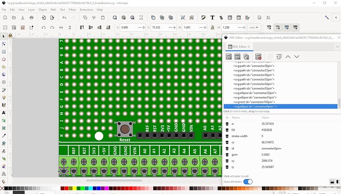
Here I started with the first terminal block and changed its id to connector0pin+ (which is not normally used and tells my python scripts that this is where to start renumbering!) Usually I would proceed in squence up the terminal block, in this case I am going to alternate with all the pins that will bus together. In this case that is the pairing. The reason for this is we are going to overlay the pins on top of each other in schematic and ordering the pins this way makes that easier to do. So instead of the REF terminal block, my next pin is on the header connector like this:
the two pins connected by the green line need to be bussed together as they connect internally to the board. Now proceed in sequence up the terminal strip (alternating with the header)
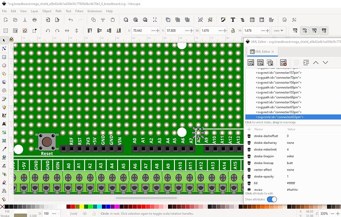
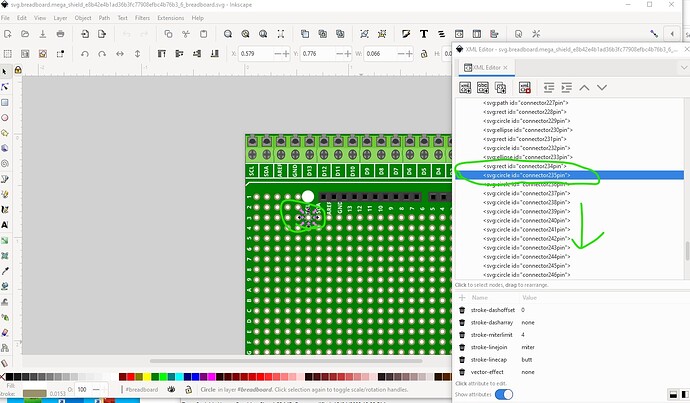
here there is a change because there is a third pin (a pad) added to the group for the next bunch of pins so we need to add another pin to the group. I have now completely reorganized the connectors (hopefully correctly)
Here I finished with a Edit->select all, Edit–>resize page to selection (to reset the viewbox to start at 0 0) then Object->group and renamed the group breadboard to make the layerId (all drawing elements need to be inside the breadboard group!)
The connectors now start at connector0, and are in random order (some are not specified as connectors even in the prototyping area!) the prototyping area starts afte the last active connector. Now I need to renumber this with a script.
Now the pins start at 0 and go up in sequence
the proto area as noted starts after the last active pin as we likely need to do something to all of them and not having them mixed in makes that easier.
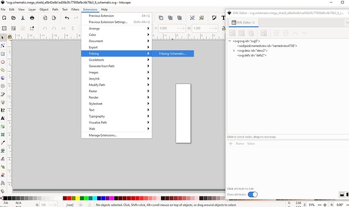
Now on to making schematic from this. Start from a empty svg (because the extension only adds things, it doesn’t delete!)
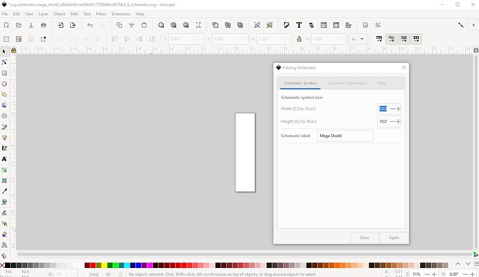
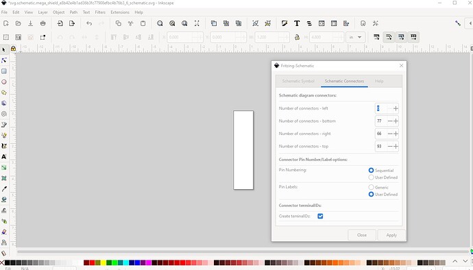
and set the parameters to do that you need to figure out how many pins on each side of the square in this case that will be 0 left (as there are no left side connectors)
left 0
bottom 77 31 terms 24 headers 8 pads 2 gnds 6 * 2 ios so 90 pins so width needs to be 9.1in
(0.1 above the number of connectors)
right 66 22 for the terms + 2 * 22 for the headers and pads.
and thus height is 11.1in to allow 110 connectors
top 93 30 pads 6 top of header 31 terms and 26 for the headers
and thus 9.4in wide. So lets set all of that.
Note that it is best to have only the schematic svg open in Inkscape when running the extension, a bug in either Inkscape or the extension (I suspect Inkscape!) causes it to sometimes write the schematic in wrong svg window if more than one is open. It is possible to copy it to the right one then delete it but only one svg is easier. So set those parameters in to the extension. Because I usually miscount I used 10 by 10 (we need to adjust the borders later anyway!) Set the board name in the title slot.
then set the number of connectors and the other parameters (such as terminalIds!) then click apply to start the extension.
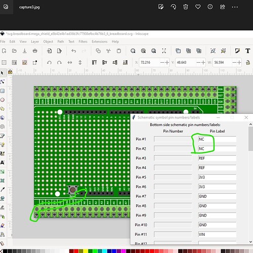
It works for a bit then puts up this screen for pin names
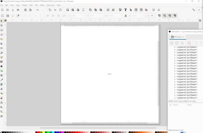
Here we need to enter every name twice to get the two bussed together pins (later we will need to do 3!) at A8 we need to do three labels each because there is an extra pin in the group. Once all the labels are entered we get an svg that looks like this
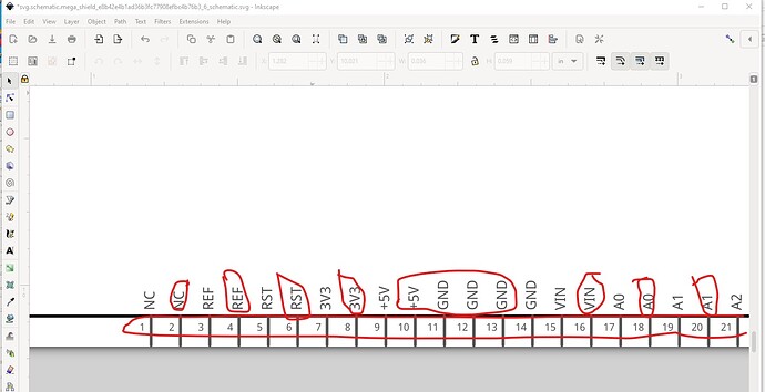
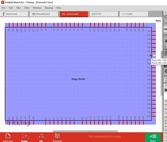
Now we need to do some editing to come up with the final (and smaller!) schematic. What we are going to do is to overlay the extra pins to reduce the size of schematic while leaving the correct pin definitions present. To do that we need to remove all pin numbers (because each pin will have multiple pin numbers and there isn’t enough space) and all the duplicate pin labels like this
everything circled in red needs to be deleted like this
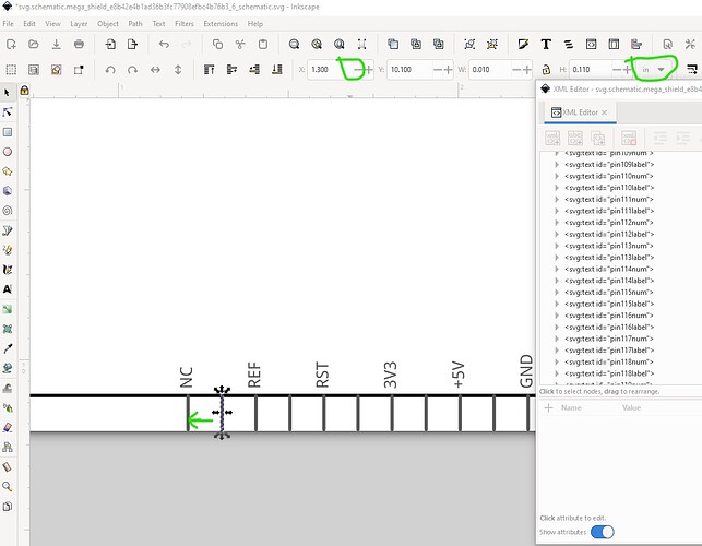
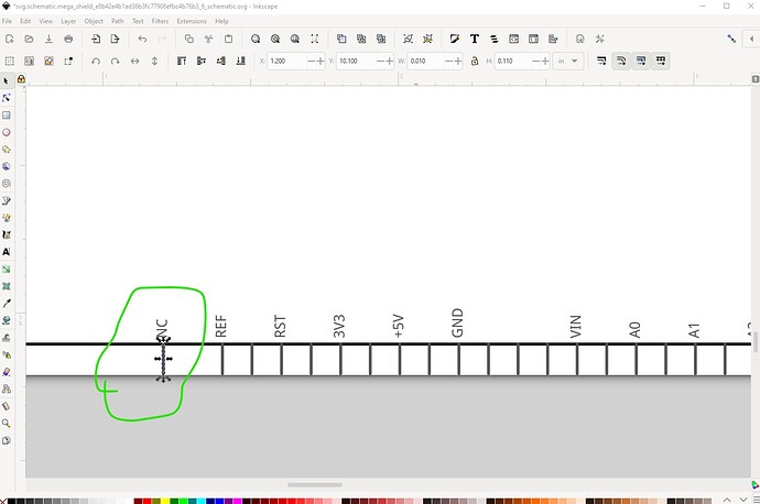
Now we need to move both the pin and terminalId
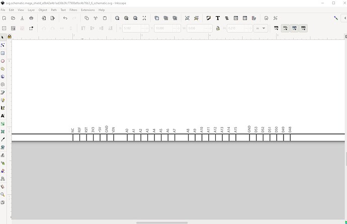
now both connector0 and connector1 are in the same place in the svg. Once they are all done we will move the combined pins so there is only 0.1in between them (thus reducing the size of schematic!)
In the end the final schematic looks like this
note none of the several hundred proto area connectors in breadboard are reflected in schematic and we will need to do something about that in the fzp file to avoid problems. Schematic is now complete so on to the .fzp file. Replace the current connectors with a set generated by FritzingCreateFzpConnectors.py
via
FritzingCreateFzpConnectors.py -n t 236
to create the 235 active connections. Substitute that for the current terminals and set the description field for all connectors. When that is finished generate the connections for the proto pins (only in breadboard) via
FritzingCreateFzpConnectors.py -n -P t 518 236
which generates 518 proto connectors starting at connector236. Append that to the end of the connectors and use a global replace to change the description to “proto pin”
then delete the entire buses section and replace it with a new hand edited (unfortunately!) bus definition set.
Add a url for where to get a board and the .fzp is done. Now run it through FritingCheckPart.py and correct any errors
Error 54: File
‘part.mega_shield_1.fzp.bak’
At line 7080
Bus nodeMember connector164 already in bus D19
only a node member error so correct that. Now checkpart runs clean
$ FritzingCheckPartw.py part.mega_shield_1.fzp
**** Starting to process file Startup, no file yet
**** Starting to process file part.mega_shield_1.fzp
**** Starting to process file svg.breadboard.mega_shield_1_breadboard.svg.bak
**** Starting to process file svg.schematic.mega_shield_1_schematic.svg.bak
**** Starting to process file svg.breadboard.mega_shield_1_breadboard.svg.bak
Warning 29: File
‘part.mega_shield_1.fzp.bak’
Processing view pcbView, File svg.breadboard.mega_shield_1_breadboard.svg.bak
has already been processed
but will be processed again as part of this fzp file in case of new warnings.
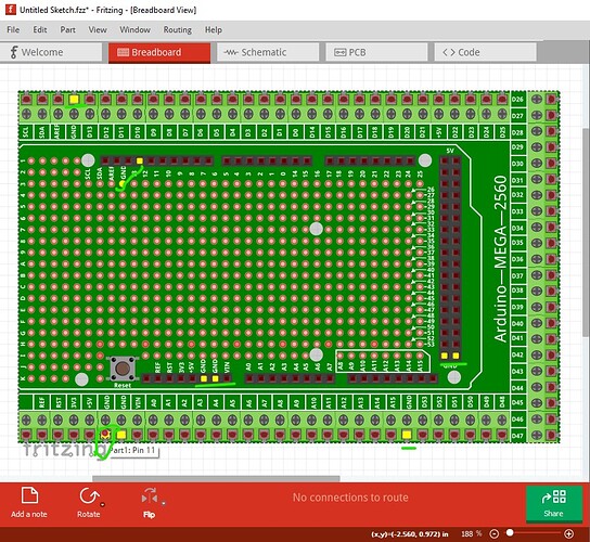
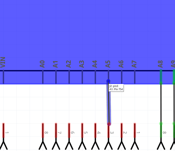
so build and test the part. Load it in to Fritzing and verify the buses are correct by clicking on each pin and make sure the correct pins light yellow like this (with ground selected)
do the same in schematic (most pins will only light up themselves as they are all overlaid, gnd and +5V are the exceptions!) As well I notice the background sometimes lights up blue. I don’t know why, it doesn’t appear to indicate an error and doesn’t always happen.
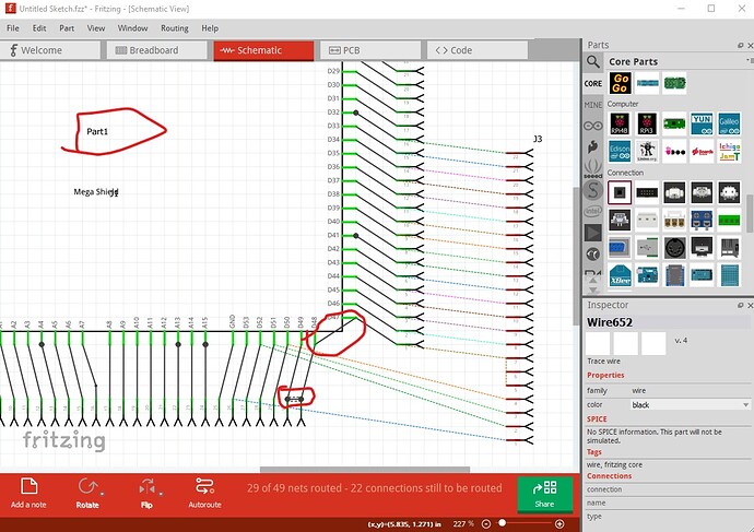
Then add headers to test every connection and make sure they are correct.In this case there are problems (probably with the order of overlaid pins in schematic)
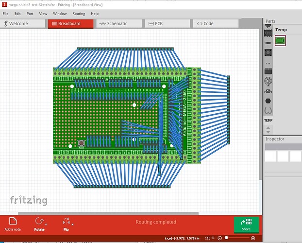
as well we haven’t set a label field which we need to correct. Here there is a short between 3 of the pins (circled in red) that needs to be corrected. It appears to have been a breadboard error, deleting and rerunning the wires corrects the problem, and a check of the part files shows no errors (which is why I deleted and rerouted the wires.) I did correct the label field in the .fzp file though (set to A for assembly.) This appears to be an instance of db corruption so save a copy of the .fzz in broken-routing.fzz in this directory to look at later. Generate a new part to pick up and test the label field and start t a new test sketch. Done and tests clean. The test sketch (included with the part below) looks pretty messy, but tests that every connection goes to where it should.
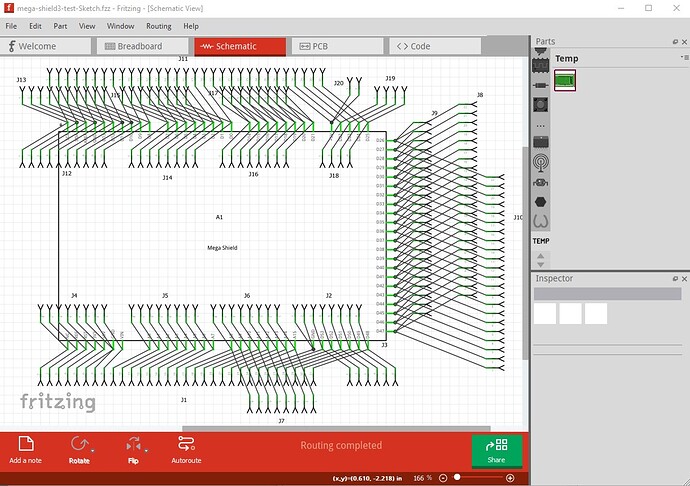
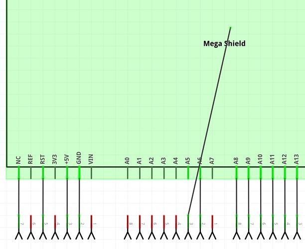
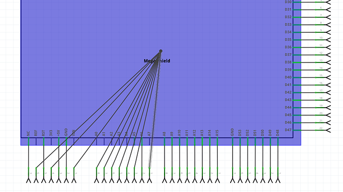
the real test is schematic to make sure all of the2 or three connections on the overlaid pins go to the correct place as it is easy to make an error here.
The wires at an angle are to verify all the terminalIds are correct (since this is Randy’ extension they all are, but I may have missed moving a terminalId with a pin which this will show up here.) Since all appears well we can declare this done with the following part and its test sketch, and I can continue on poking at the routing bug and a couple of undo issues I found during this.
mega-shield3.fzpz (171.8 KB)
and the test sketch
mega-shield3-test-Sketch.fzz (244.9 KB)
If you have questions don’t hesitate to ask!
Peter
