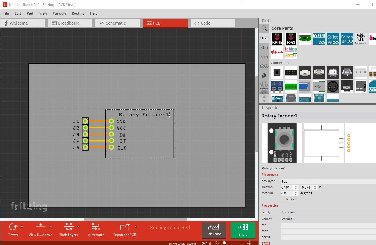
I have tried creating a 5 custom made parts for my project. 4 work well, One is killing me. The one that is killing me is a common rotary encoder used in arduinos.
there is one here, but it is for 90 degree headers. My part has straight through headers, so I decided to build my own part. I am getting the aforementioned error and autoroute is also not routing across the top and bottom of the PCB. I have created a gerber file and used gerblook to visualise the PCB. The holes are drilled properly, the copper is on TOP and bottom layers, soldermask is on both layers, everything looks proper in the gerber, but the PCB is not routing across top and bottom. It is using vias. KY-040_M274_Encoder.fzpz (8.1 KB)
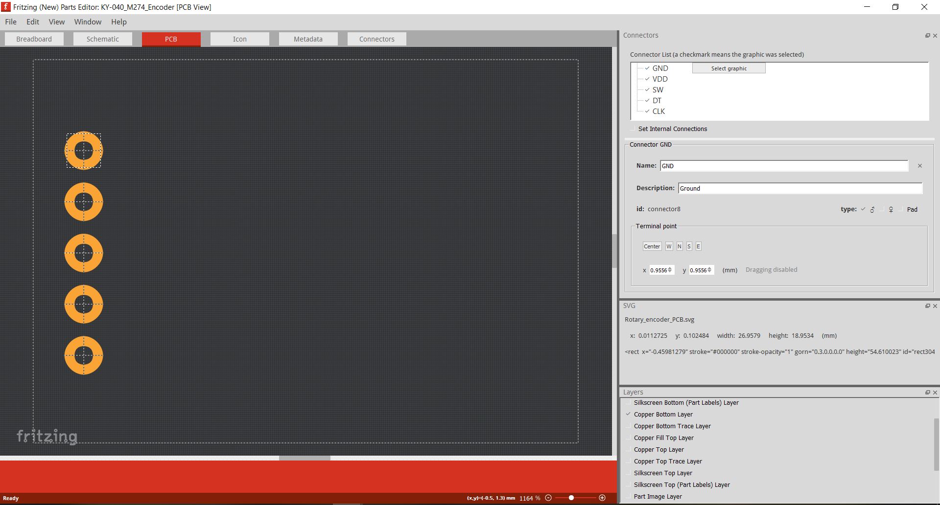
The svg has two groups, copper1>copper0>(connectorpads).
All my other parts also have the same PCB SVG format and they work pretty well.
I looked at the fpz file(using an xml editor). I noticed that the connector pads were only on one layer.
I edited the fpz file manually to include the pads on both layers, but when I try to import the file into fritzing, I get an error that says Unable to import part.
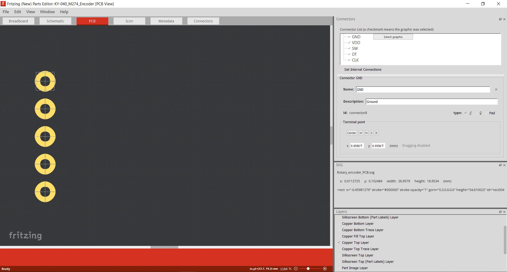
Looking at the part in Part editor mode, PCB view, If I hide all layers and then show copper Top and copper Bottom, I am able to see the copper in both layers. Why is it not working then?
The problem with this second part is that it contains a folder instead of files (you compressed the containing folder instead of the files inside): once you fix it, the part can be imported normally.
In any case, the part has some other issues that @vanepp (probably) will explain better than me.
which has an improved version later in the post. That said, as @roboteach said your zip file is the entire folder which is why the part won’t load. To correct that zip only the files to a .fzpz file and it will work. Doing that indicates a number of errors: schematic lacks terminalIds which causes this:
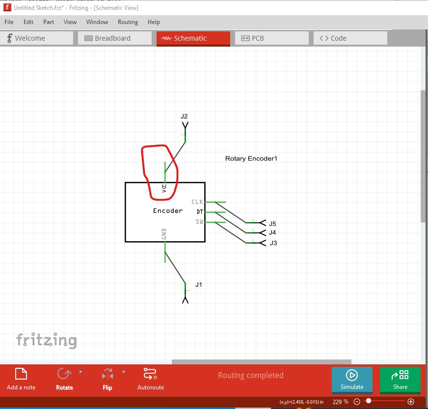
where the wire connects to the middle of the connector rather than the end as it should. As well in pcb the hole sizes are incorrect (and inconsistent):
The no layerId errors mean that your part won’t export as an image, the rest should be self explanatory. The following tutorial may help you in correcting the errors:
I saw that part and mentioned it in my first letter. But that part is for 90 degree header pins breakout board, not for a straight pins breakout board which is what I need for my project. If someone can point me towards a straight pin version, I’ll be very happy.
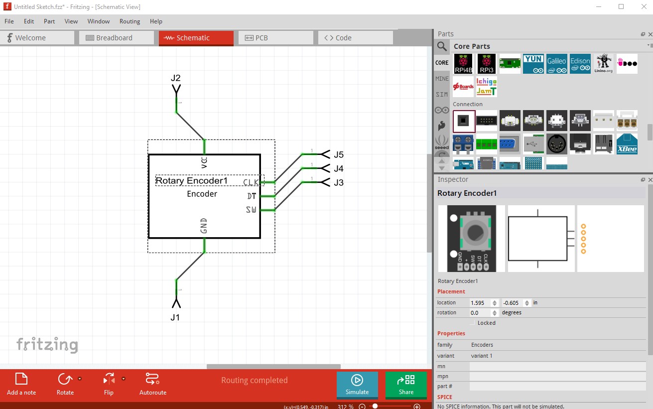
Is the issue with schematics a deal breaker? Is it going to be a big problem in the future? coz this is how my schematic looks right now:
The connection is at the centre as you mentioned, but it conveys the message pretty well enough is what I am thinking. Unless I’m missing some really important use case of the schematic, like automated PCB design capabilities with other softwares or something.
The top two entries
T100C0.035870
T101C0.035871
should match the third
T102C0.038000
which is the correct size for a 0.1in header. The 0.035in holes are too small.
How do I get the hole sizes to match? All the holes are of the same size in the SVG files. Why the difference in gerber then??
@roboteach I re-zipped the file and for now, the major issues are sorted.
Thank you.
If anyone wants, here are the parts I made. They are purely functional. Absolutely non-aesthetic. Free to use by everyone, just like fritzing. Have a few rough edges, just like fritzing .
The terminalIds are not fatal, as you see, it will connect fine to the middle of the pin. The missing layerIds aren’t fatal, but your part won’t appear in the image if the sketch is exported as an image, again not fatal if you aren’t using images of the sketch. As to the pad sizes, assuming you are using Inkscape, the hole size is
hole_size = pad_diameter - (2 * stroke-width)
as the svg scale is odd, I copied in a correct pad to the pcb svg and then displayed it.
The radius should be 2.0880003 and the stroke-width 1.44 to make the pad hole the correct 0.038in. I fixed up the layerIds and modified schematic to add the terminalIds to make this part which should be correct: