Hello here is a KF142R clamp terminal block in 2 pin
KF142R-5.08-2P.fzpz (6.7 KB)
![]()
Hello here is a KF142R clamp terminal block in 2 pin
KF142R-5.08-2P.fzpz (6.7 KB)
![]()
Welcome aboard! Unfortunately parts creation is fairly complex and your part has several problems. This tutorial covers most everything I did here if you haven’t seen it already.
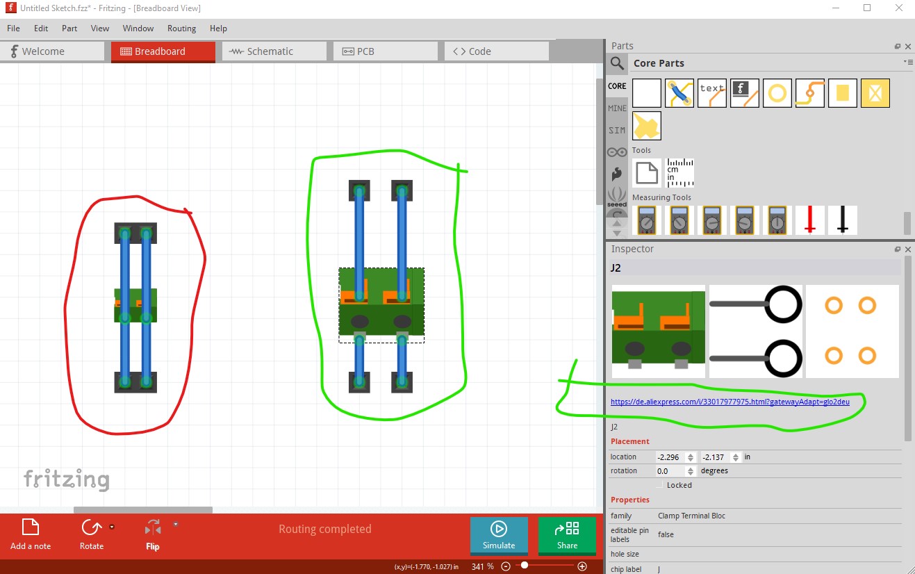
That said, on to your part. Breadboard view should reflect the actual size of the part. I took the dimensions from this site (which may or may not be correct!)
https://de.aliexpress.com/i/33017977975.html?gatewayAdapt=glo2deu
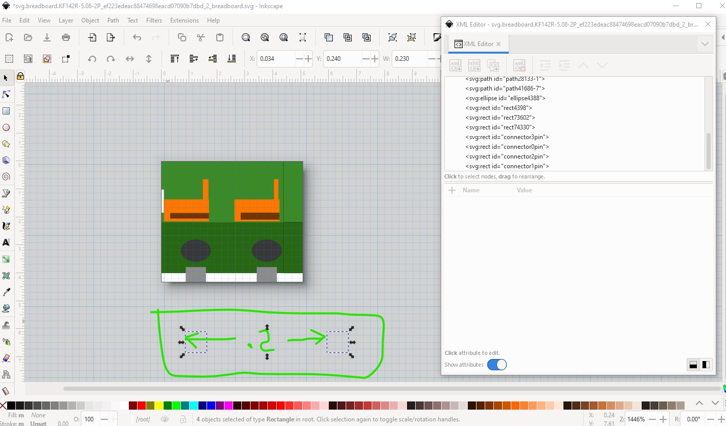
Here I added two pins spaced 5.08 (0.2in) apart as we see the current breadboard view is about half the size it needs to be.
so I basically doubled the size of the image (leaving the pins as is as they are correct) and then moved the pins in to the correct position.
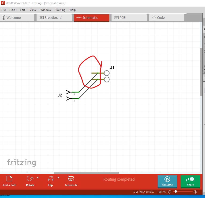
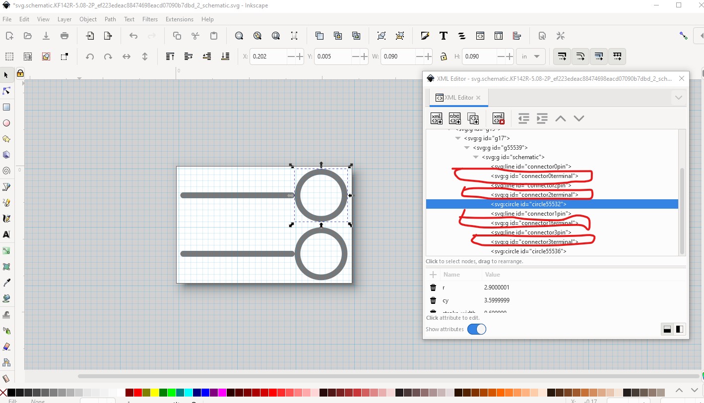
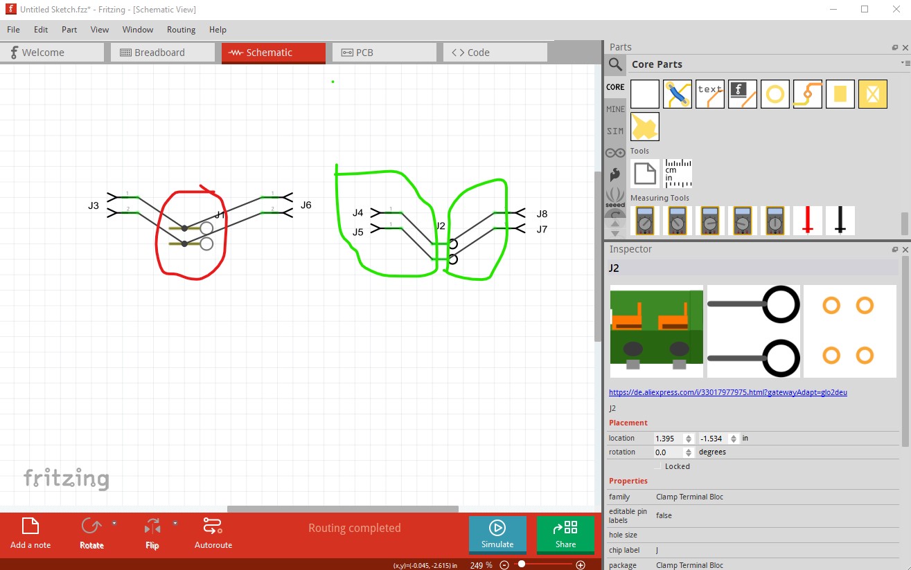
I also split the pins to not be on top of each other but one set above the other and then bussed them together so both pins have an internal connection (as they do in real life!) In schematic in Fritzing we see that the wire is connecting to the middle of the pin rather than the end. This is because the terminalId in the schematic svg is a group (with no drawing elements) and thus Fritzing doesn’t recognize it as a terminalId and connects the wire to the middle of the pin.
this is the schematic svg displayed in Inkscape with the offending groups circled in red.
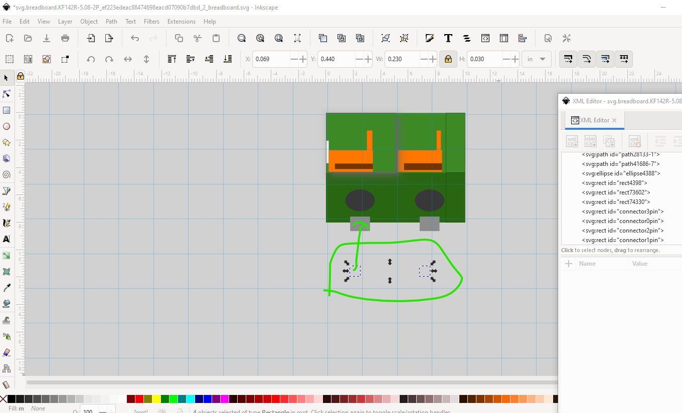
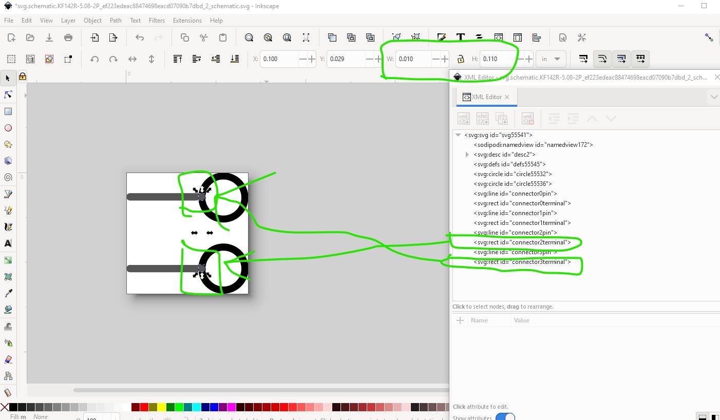
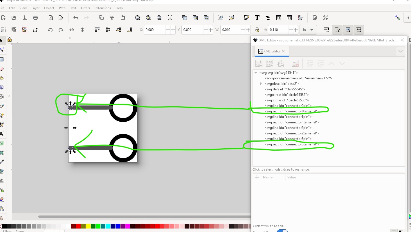
This is the same svg with the terminalIds replaced with 10thou by 10thou rectangles and positioned on each end of the pin so the wires will connect to the end of the pin as desired.
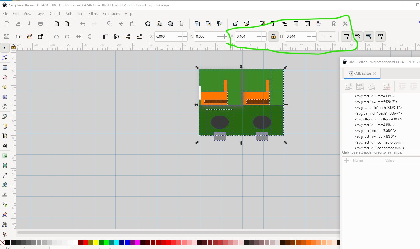
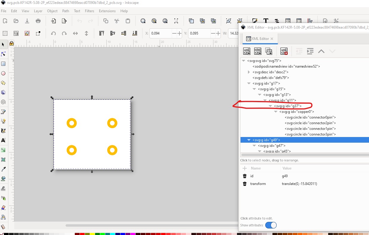
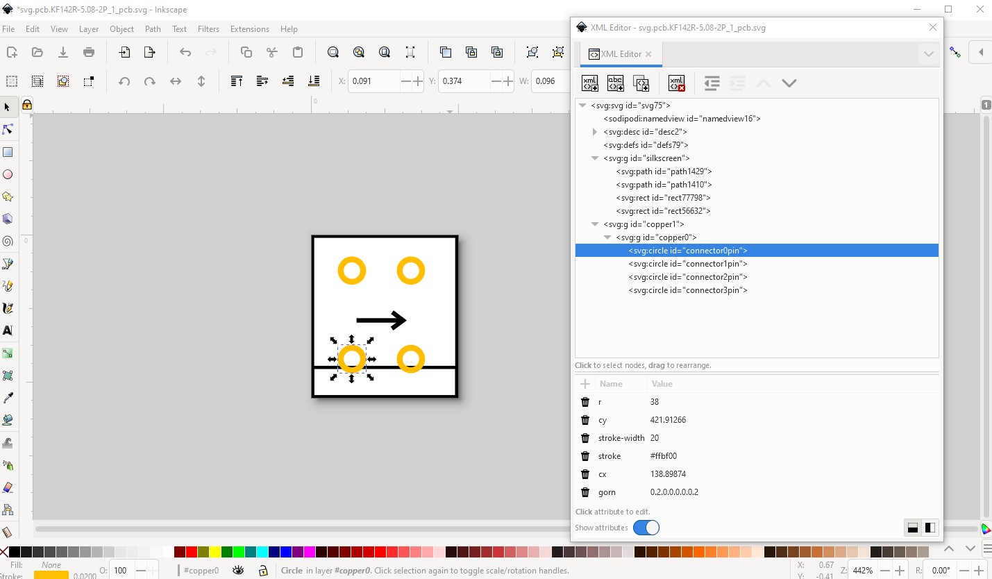
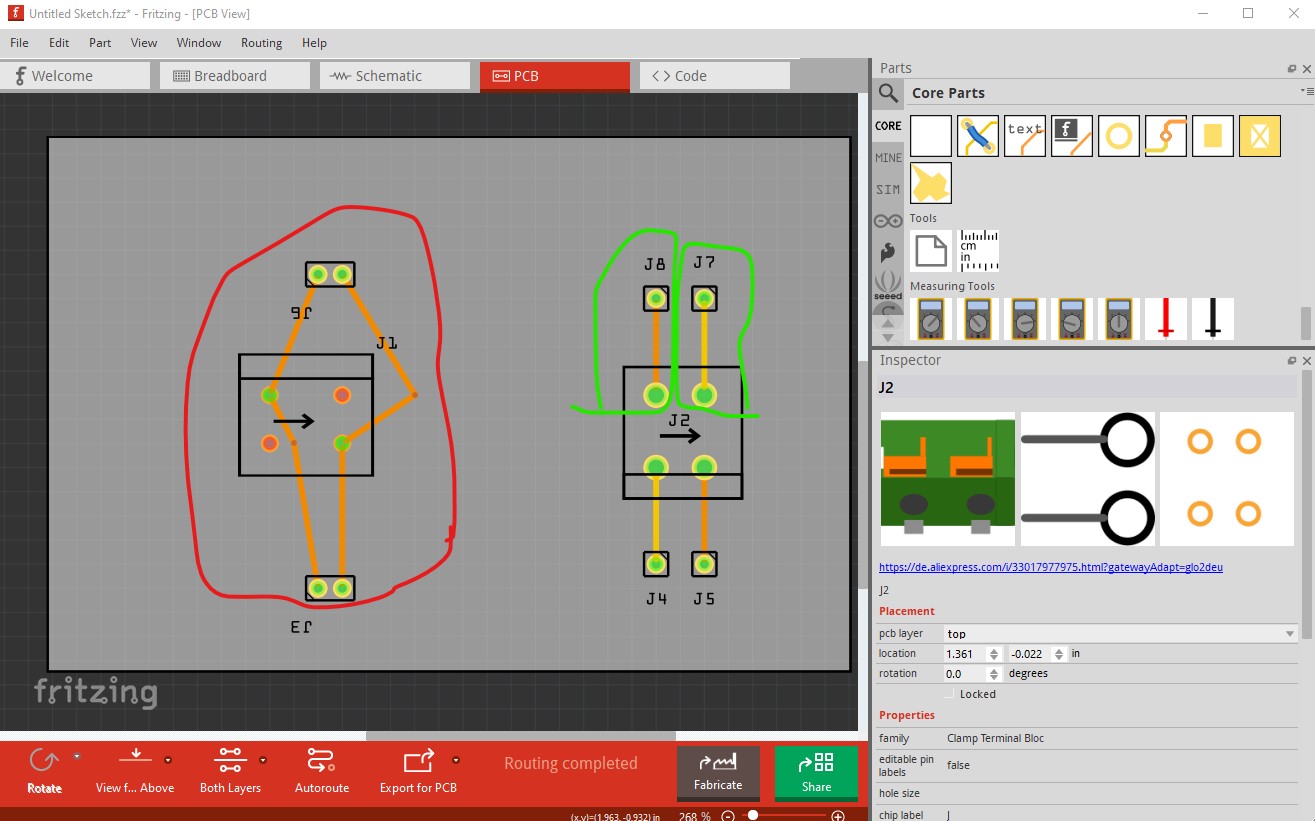
This is the pcb svg from your part. It is missing the copper1 group name and thus will only connect on the bottom layer not the top (which is copper1) replacing the group name with copper1 would fix this.
in addition the hole size is not sufficient for the pins, the data calls for a 1.4mm (approx 0.056in) hole, the hole here i 0.035in and thus too small. The hole size (in Inkscape) can be calculated as
hole_size = pad_diameter - (2 x stroke-width)
with the set .02in stroke width that means we need a 0.096in pad size to get the desired 0.056 hole in the gerber output.
as well the silkscreen didn’t reflect the actual size of the part that has been corrected here.
The part on the left is your original, the one on the right is my corrected version
note your part connects to the center of the pin, mine to each end of the pin but the pins are bussed together so there is an internal connection between the header connectors.
In pcb above all the wires connect to only 2 pins (because the connected ones are not bused) and will only connect on the bottom layer (because copper1 is missing.) Neither is true of my part. Here is a copy of my part, if you unzip the .fzpz file you will get the .fzp and all the svg files so you can see what changes I made.
KF142R-5.08-2P-improved.fzpz (4.5 KB)
feel free to ask about anything that isn’t clear!
edit: The gerber output (specifically the drill.txt file) gives the hole size as 0.056in via the T100C0.056000 line, where t100C is the hole label and 0.056000 is the hole size in inches.
; NON-PLATED HOLES START AT T1
; THROUGH (PLATED) HOLES START AT T100
M48
INCH
T100C0.056000
%
T100
X014222Y014777
X014222Y011777
X012222Y011777
X012222Y014777
T00
M30
Peter
Hello and thank you for all the corrections with the explanations of my errors
This was my first component where I started from the existing component base to modify them
I will go over the tutorial to improve myself