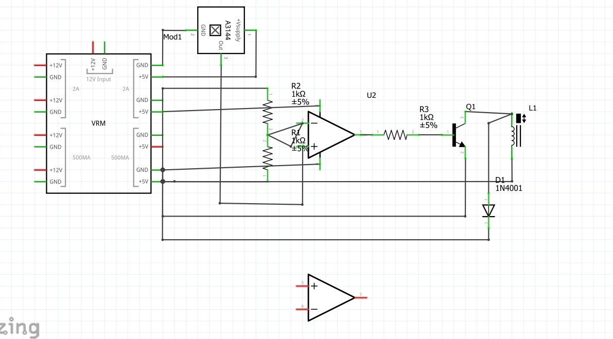
So im absolutely new to fritzing and circuit designing and i do not know how to make a voltage divider for a lm358 , i cant understand how to make it . for context im making a circuit for a maglev train project where i have to detect the magnetic field strength and adjust an electromagnet . when the magnet rises too high, the voltages will change accordingly, can someone PLEASE help me i dont know anything;-;. Thank you in advance .
(P.S: sorry for my bad english its not my 1st language)

@Monke please attach .gas sketch file
If you need parts, please post a request under a separate topic in parts help and fill up the template
(Unrelated: I’ve moved your topic to projects)
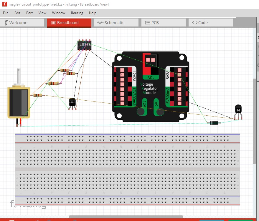
maglev_circuit_prototype.fzz (18.9 KB)
here you go sir, and thank you so much for helping me
Hi @Monke
Many problems here.
1. Bad connections
For example here
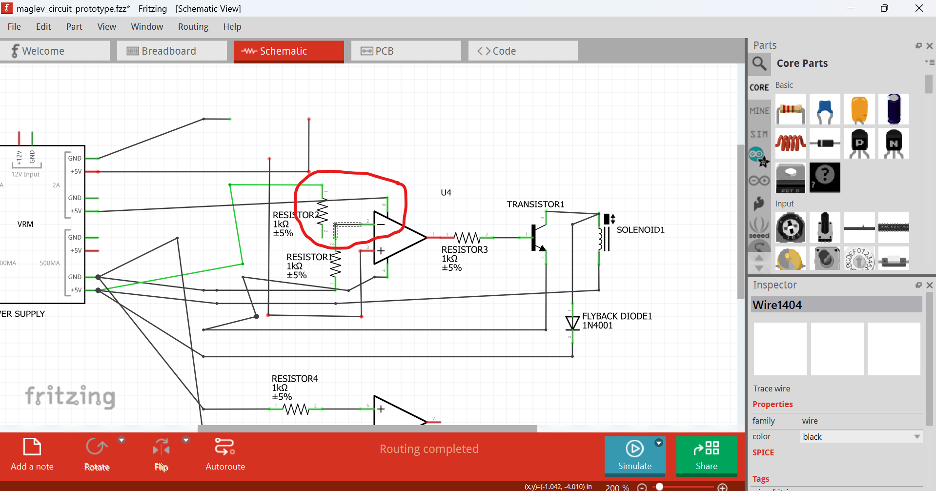
Let’s zoom in to the problem
In this picture here

It looks like the resistors and the ‘-’ terminal of the AMP are connected together.
However, if you drag RESISTOR1 to the right, you’ll see this
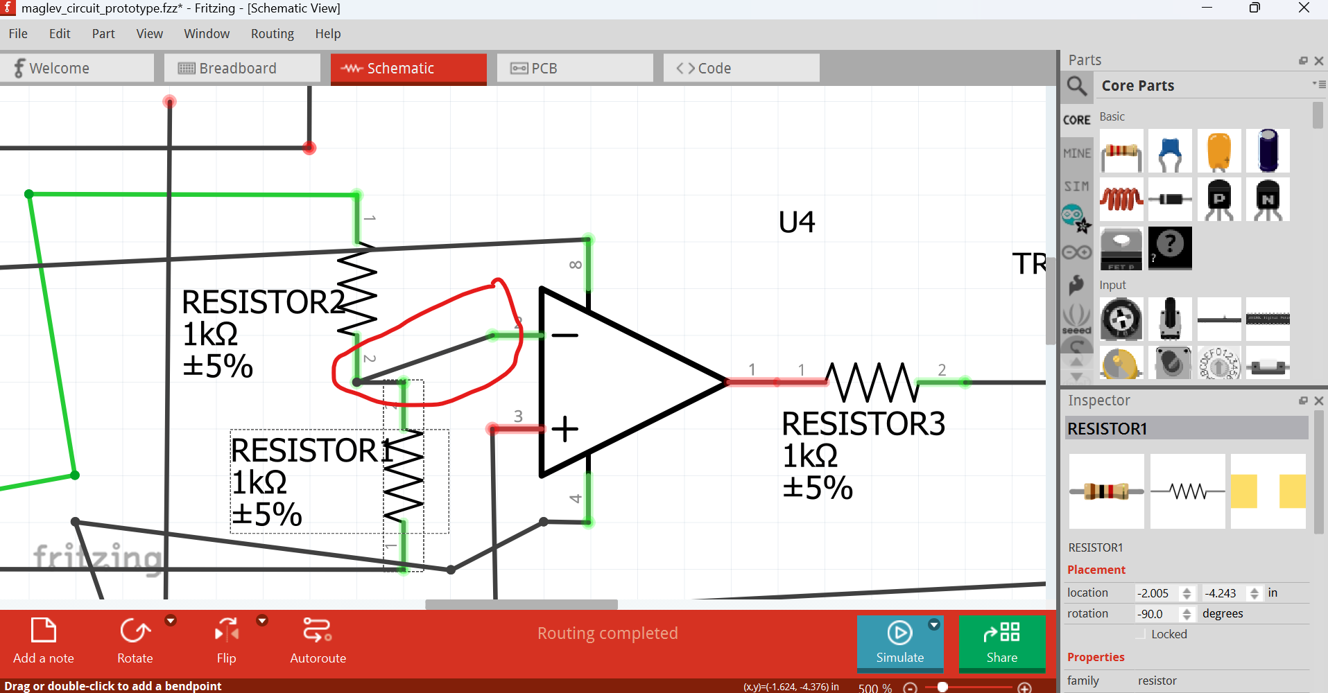
Yes, they are connected. However these are cold connections.
To fix, delete the trace and route like this (as you can see the blue wire)
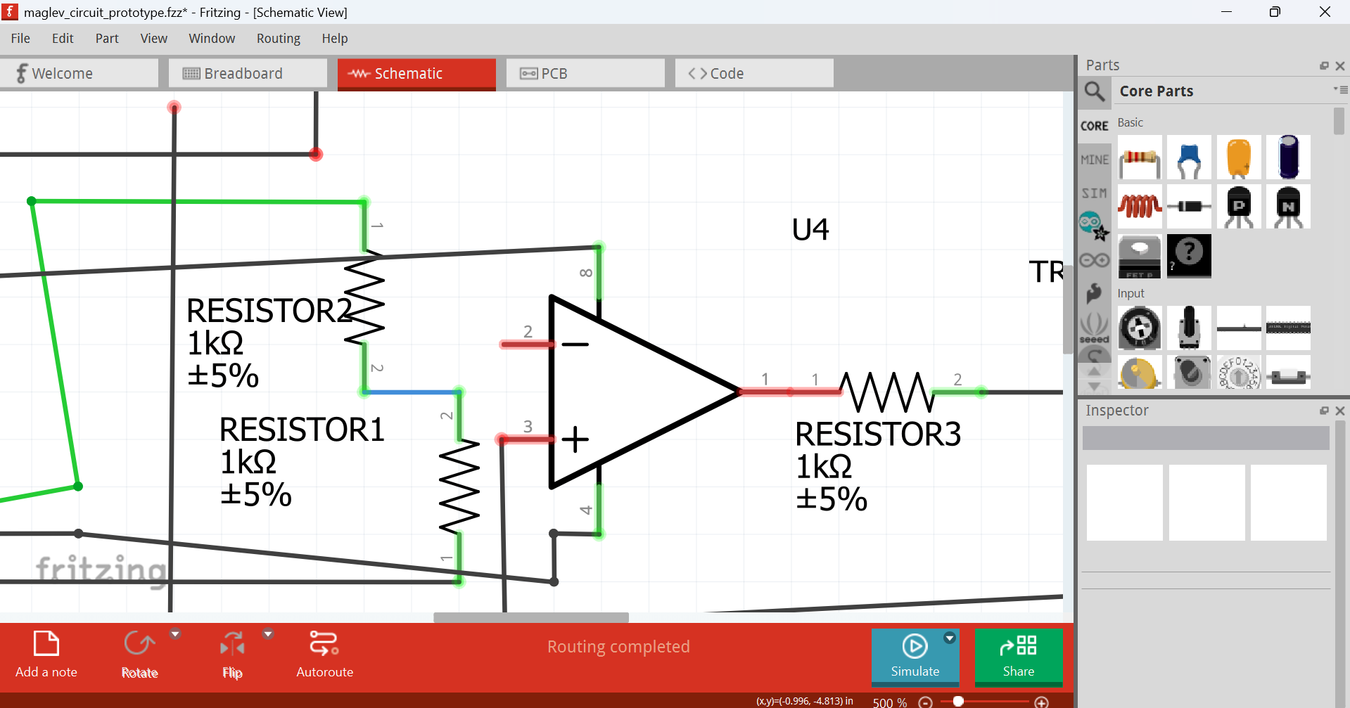
Create a bendpoint in the middle
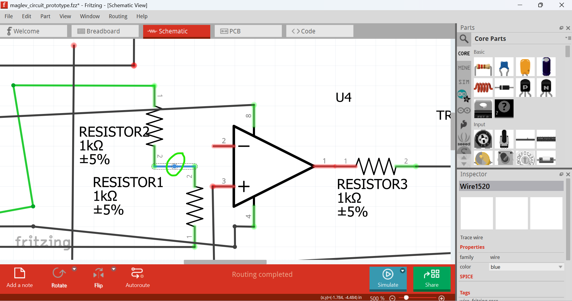
Route a wire from ‘-’ to the bendpoint
Now this is a proper connection
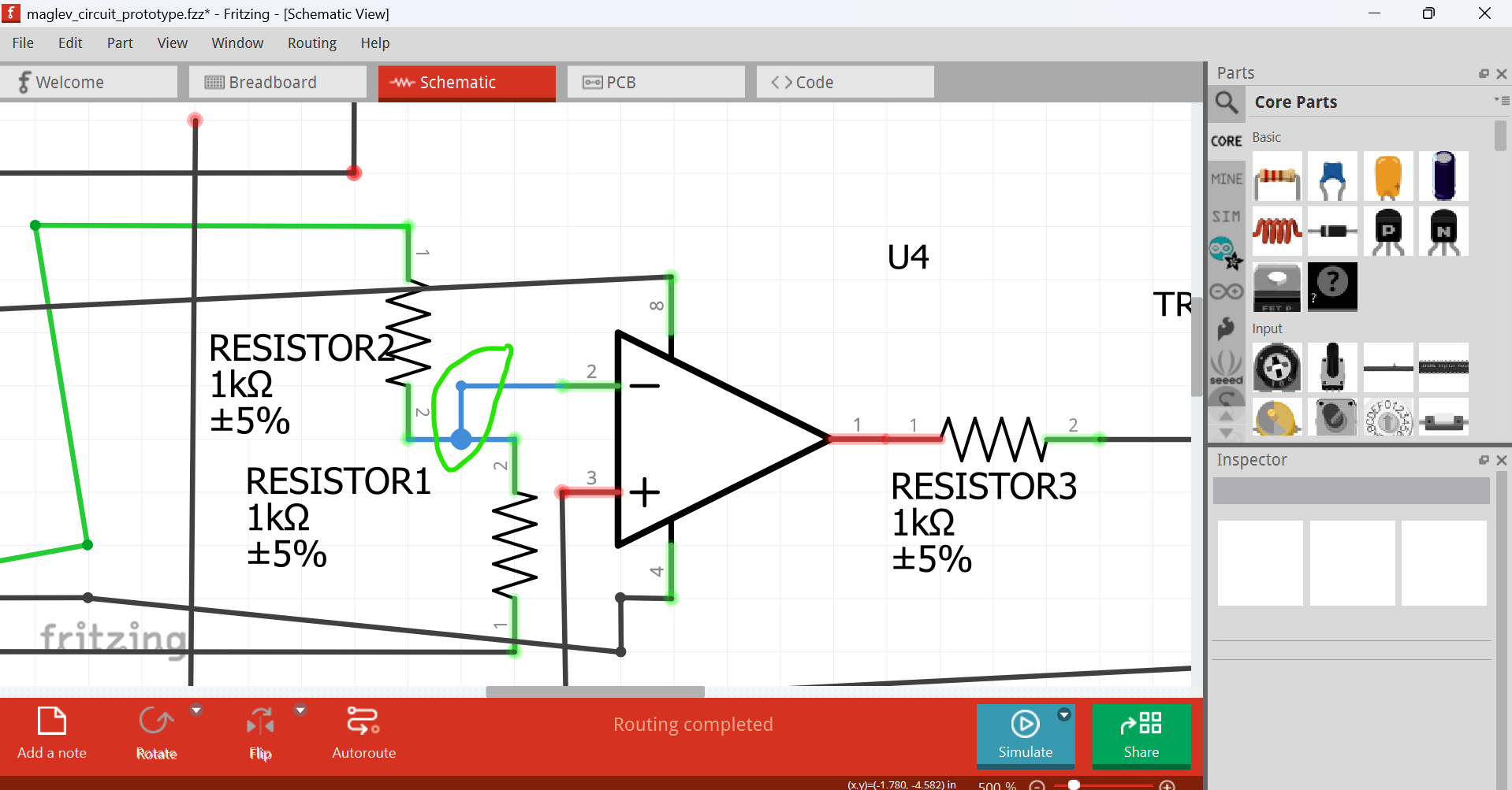
To make things neater
A little uglier though
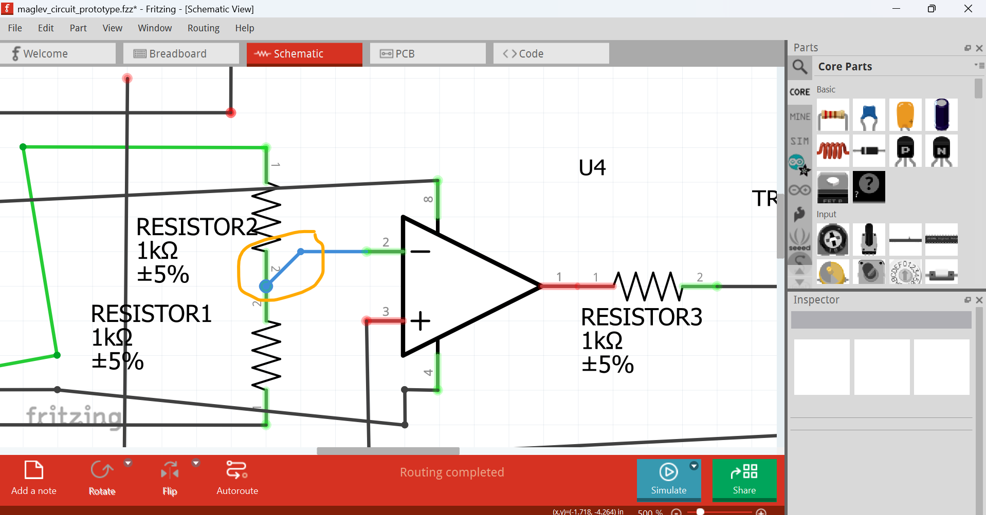
There are more problems taht I’m discovering now.
This is also suspicious
(as you can see the red cable)
maglev_circuit_RAPTOR7762.fzz (16.8 KB)
I’ll post this file and see if anyone can help
@Monke You dn’t have to reply in English. Though preferred, you can reply in any other language (your native language)
oh my god thank you so much im so dumb i didnt even know that my voltage divider was bad , thank you soso much for teaching me ;-; . thank you for uploading a new diagram as well sir
Thank you
also i dont think it would help if i asked my qs in bengali lol thanks though
bengali isn’t an issue, we have google translate /chatAGP which will translate it in to English (or whatever language) for us. Clarity is the more important part and using your native language helps with that. Your original sketch is very badly broken (I’m currently recreating it from scratch as it isn’t recoverable), what Fritzing version are using? I have never before seen a sketch this badly corrupted, breadboard view is totally non functional. Also do you want SMD resistors in pcb (as opposed to through hole? It is easy to change later in any case (although it affects routing.)
Peter
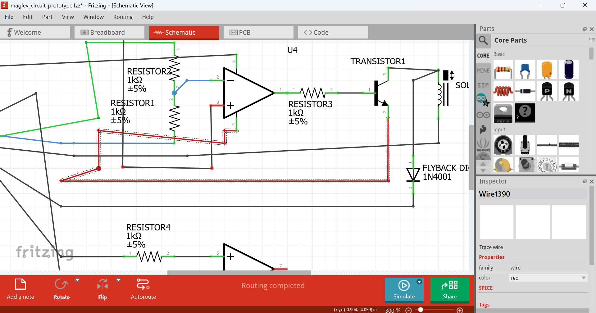
Since you are redoing it from scratch, probably does not matter, but that red line at the op amp plus usually means that the trace ending there is not really connected.
OK here is a corrected version of your sketch (although I didn’t route breadboard.)
maglev_circuit_prototype-fixed.fzz (23.3 KB)
I exported the hall effect part from your sketch and added it to the new one, then dragged in the parts in use from core parts (this is on Fritzing 1.0.5.) Breadboard now works although I haven’t routed it the rats nest lines will show where the connections should go if you want to route it.
I actually started from schematic like this. I dragged in the schematic ground part from core parts schematic and a power net part (and then set it’s voltage to 5V in Inspector the lower right window) and used them for power and ground.
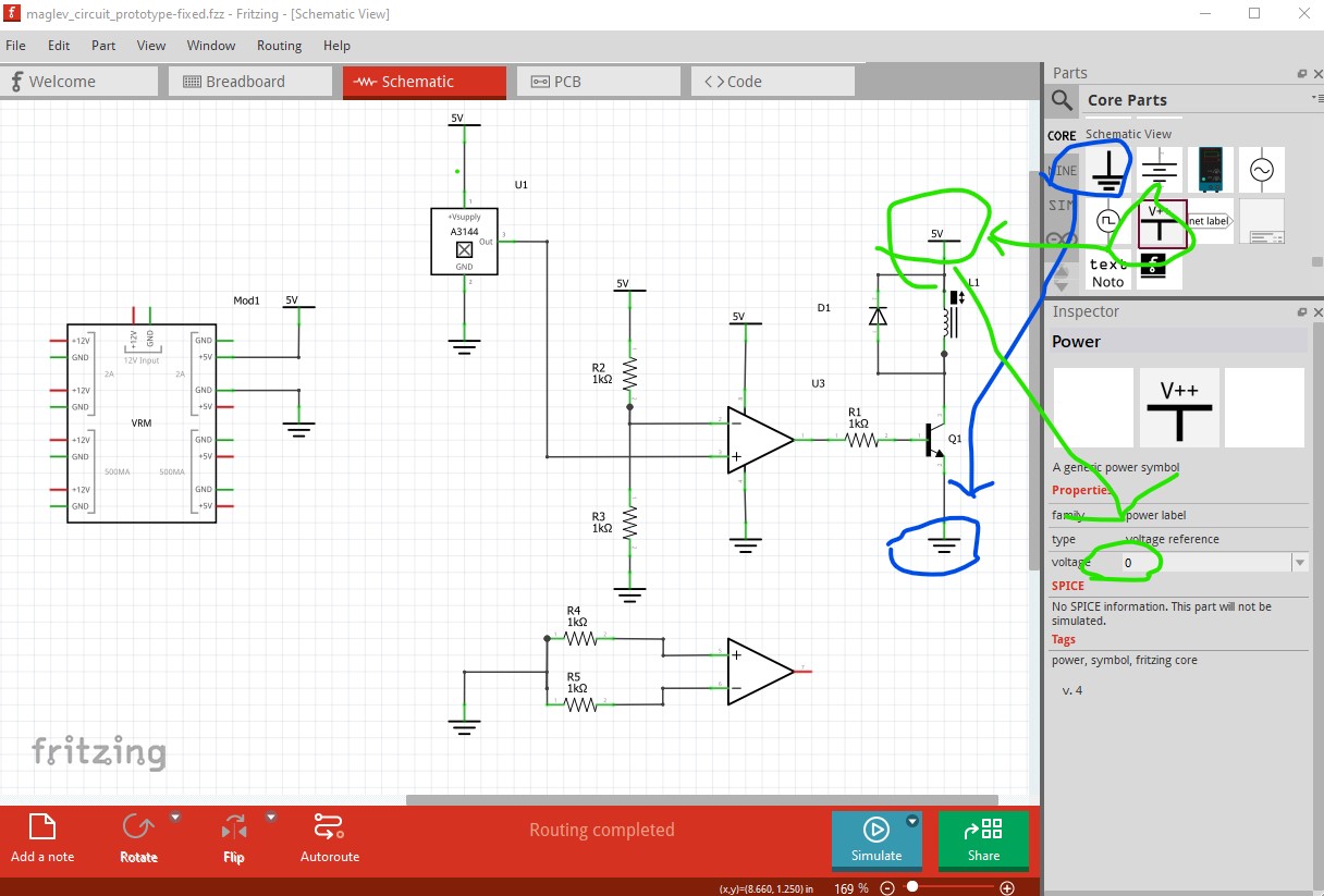
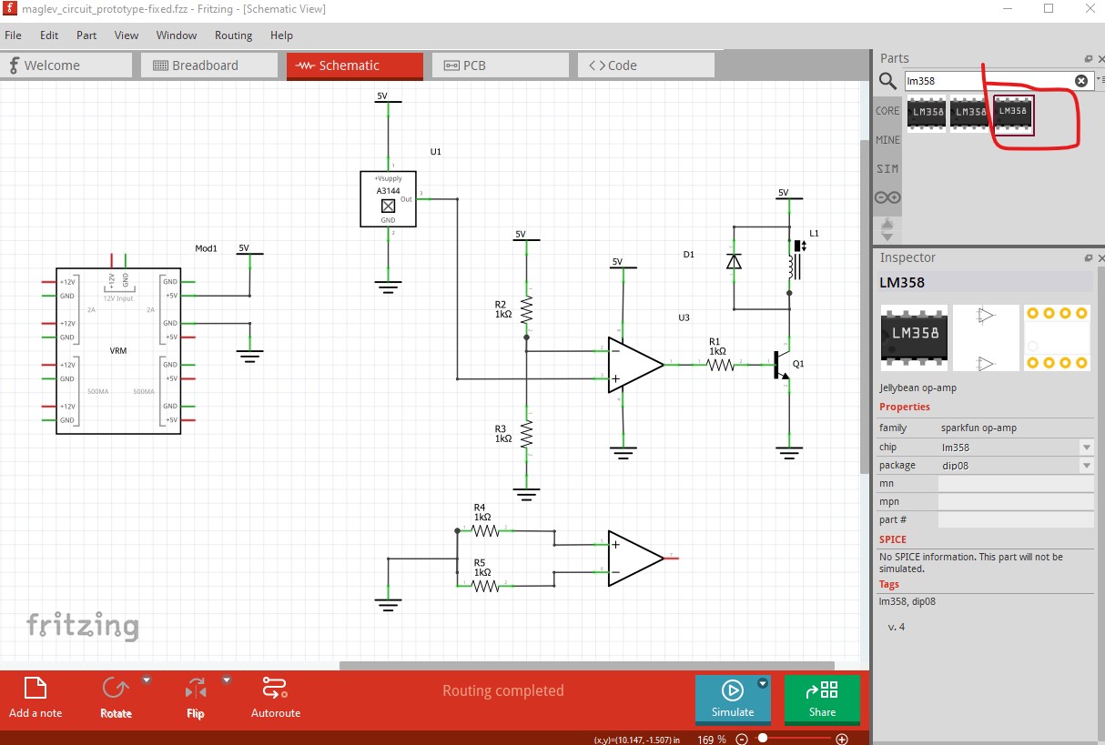
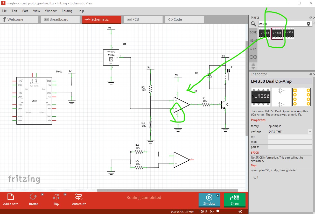
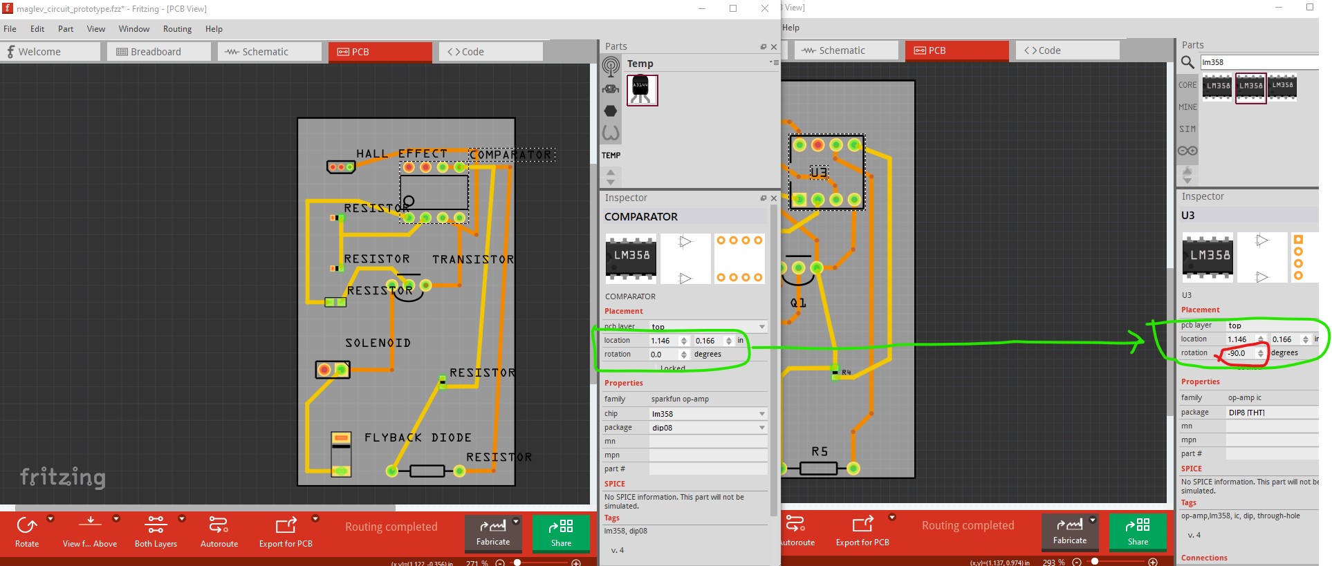
The original op amp you used is a bad choice as it has issues with pins being not on the grid in schematic. There is a corrected version available in core parts and I used that. This is the incorrect one, beside it is the corrected version which I used.
As you see the wires connect correctly to the pins on this version.
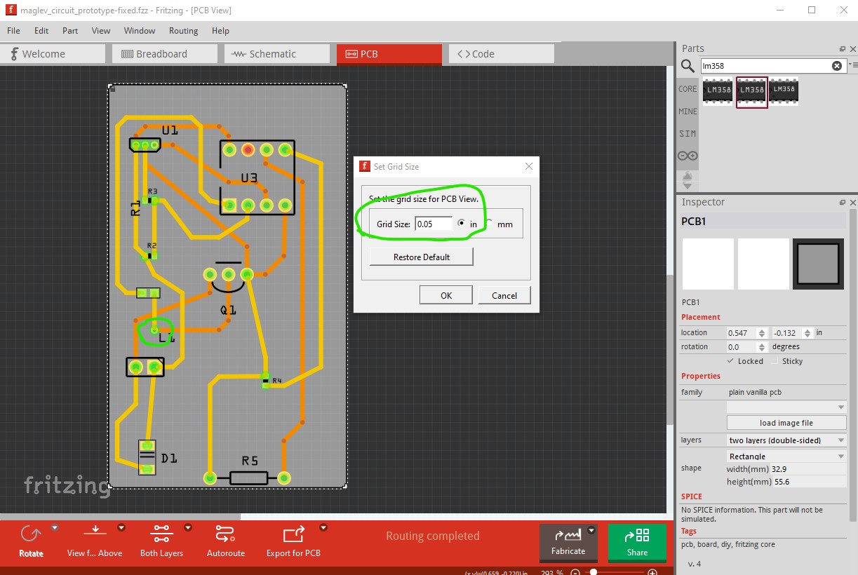
Then I routed pcb. I needed to reduce the grid size to 0.05in (from 0.1in) to get routing to work correctly. I assumed that your current layout is necessary for some reason, if not then you can simplify things by changing the SMD resistor to THT which would make routing much easier. Since you have both THT and SMD resistors it isn’t clear to me it that is intentional or by accident (although THT is the default so I a assumed intentional. I needed to use one via (circled in green here) to get routing to work. With THT resistors which can route on either side of the board, that could be eliminated.
for @RAPTOR7762 's information, in order to replicate his pcb layout I did this: First set the pcb board size and location identical to his, then with the original sketch in one window, copy the location and orientation information from the original sketch to the new one. That places the parts (sometimes with a different orientation to make the connections come out correctly) in the new board then route it.
hope this helps.
Now I will try google translate to translate this in to bengali
Peter
via google translate
ঠিক আছে, তোমার স্কেচের একটি সংশোধিত সংস্করণ এখানে দেওয়া হল (যদিও আমি ব্রেডবোর্ড রুট করিনি।)
maglev_circuit_prototype-fixed.fzz (২৩.৩ KB)
আমি তোমার স্কেচ থেকে হল ইফেক্ট অংশটি এক্সপোর্ট করেছি এবং এটি নতুনটিতে যুক্ত করেছি, তারপর মূল অংশগুলি থেকে ব্যবহৃত অংশগুলি টেনে এনেছি (এটি ফ্রিটজিং ১.০.৫-এ রয়েছে।) ব্রেডবোর্ড এখন কাজ করে যদিও আমি এটি রুট করিনি। ইঁদুরের বাসার লাইনগুলি দেখাবে যে সংযোগগুলি কোথায় যাওয়া উচিত যদি আপনি এটি রুট করতে চান।
আমি আসলে এই ধরণের স্কিমেটিক দিয়ে শুরু করেছি। আমি কোর পার্টস স্কিমেটিক এবং একটি পাওয়ার নেট পার্ট থেকে স্কিমেটিক গ্রাউন্ড পার্ট টেনে এনেছি (এবং তারপর নীচের ডান উইন্ডোতে ইন্সপেক্টর থেকে এর ভোল্টেজ 5V তে সেট করেছি) এবং পাওয়ার এবং গ্রাউন্ডের জন্য সেগুলি ব্যবহার করেছি।
আপনার ব্যবহৃত আসল অপ অ্যাম্পটি একটি খারাপ পছন্দ কারণ এতে স্কিমেটিকের গ্রিডে পিন না থাকার সমস্যা রয়েছে। কোর পার্টসগুলিতে একটি সংশোধিত সংস্করণ পাওয়া যায় এবং আমি এটি ব্যবহার করেছি। এটি ভুলটি, এর পাশে আমি যে সংশোধিত সংস্করণটি ব্যবহার করেছি তা রয়েছে।
আপনি দেখতে পাচ্ছেন যে তারগুলি এই সংস্করণের পিনের সাথে সঠিকভাবে সংযুক্ত।
তারপর আমি পিসিবি রাউট করলাম। রাউটিং সঠিকভাবে কাজ করার জন্য গ্রিডের আকার 0.05in (0.1in থেকে) কমাতে হয়েছিল। আমি ধরে নিয়েছিলাম যে আপনার বর্তমান লেআউটটি কোনও কারণে প্রয়োজনীয়, যদি না হয় তবে আপনি SMD রেজিস্টারকে THT তে পরিবর্তন করে জিনিসগুলি সহজ করতে পারেন যা রাউটিংকে অনেক সহজ করে তুলবে। যেহেতু আপনার কাছে THT এবং SMD উভয় প্রতিরোধকই আছে, তাই আমার কাছে স্পষ্ট নয় যে এটি ইচ্ছাকৃত নাকি দুর্ঘটনাক্রমে (যদিও THT ডিফল্ট তাই আমি ধরে নিচ্ছি যে এটি ইচ্ছাকৃত। রাউটিংটি কাজ করার জন্য আমাকে একটি via (এখানে সবুজ রঙে বৃত্তাকারে দেখানো হয়েছে) ব্যবহার করতে হয়েছিল। THT প্রতিরোধকগুলি যা বোর্ডের উভয় পাশে রুট করতে পারে, এটি বাদ দেওয়া যেতে পারে।
@RAPTOR7762 এর তথ্যের জন্য, তার পিসিবি লেআউটটি প্রতিলিপি করার জন্য আমি এটি করেছি: প্রথমে পিসিবি বোর্ডের আকার এবং অবস্থান তার মতো সেট করুন, তারপর একটি উইন্ডোতে মূল স্কেচ দিয়ে, মূল স্কেচ থেকে অবস্থান এবং ওরিয়েন্টেশন তথ্য নতুনটিতে অনুলিপি করুন। এটি নতুন বোর্ডে অংশগুলি (কখনও কখনও সংযোগগুলি সঠিকভাবে বেরিয়ে আসার জন্য একটি ভিন্ন ওরিয়েন্টেশন সহ) রাখে এবং তারপরে এটিকে রুট করে।
আশা করি এটি সাহায্য করবে।
এখন আমি এটি অনুবাদ করার জন্য গুগল অনুবাদ চেষ্টা করব …
পিটার
ahhh ookay thenn, im using the fritzing 1.0.5 as well but idk how they all got corrupted , alsois there a difference between smd resistors as opposed to through hole ? tbh through hole would be the better opption for me since its a diy project for school
oh my god this is pretty good bengali haha! but ill be as comfortable as everyone else using english, thanks a lot though!
ahhh now i understand the problem with my pcb lol , thank you so much , i didnt check the size of it at all! thanks a lot
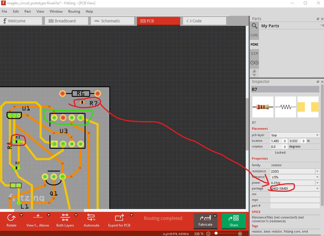
Yes there is a big difference between the two. The THT version looks just like the resistor in breadboard

and will accept connections on the top and bottom of the board (making routing without vias much easier. The SMD 402 parts you used look exactly small as the image in pcb and are hard to hand solder, As well they only connect on the side of the board they are on (top or bottom) as that is the only place they have a connection (no hole between layers without a via) making routing more difficult.

To change the SMD resistors back to through hole, go in to Inspector (the lower right window) and click on the package icon and select THT from the drop down menu. That will change the resistor to through hole like the one in breadboard (the breadboard image doesn’t change for THT or SMD which is somewhat confusing.)
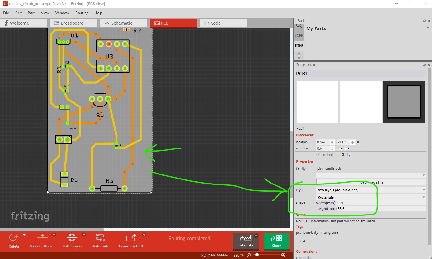
To set the size of the board click on it in pcb and again in Inspector change the size
edit:
As well I expect it would be a good bet to uninstall and reinstall Fritzing as I suspect your installation is damaged because as I said I have never before seen a sketch as badly corrupted as that one. On the older versions (before about 1.0.2 I think) there was a bug that sometimes badly corrupted sketches but that is mostly fixed in the latest versions (and in any case didn’t do what ever happened to your sketch!) If you have any idea what you did and can recreate it (fairly unlikely I think, it took me more than 5 years to recreate the original corruption bug!) I would be very interested in what you did so we can get it fixed!
Peter
ahh i probably must have been confused with tht and smd , and lemme reinstall fritzing so that this problem doesnt ever occur again lol, thank you!
Same here, the example from @Hans_Werner_Atzenhoe was complicated to properly report a bug in any case
welchen Fehler gemeldet?