Just wanted to say a big thanks for the pi-hat part! Started working on one today! 
On the edge of off topic, what is the best way of routing from the outer edge of the pins… try to fit them between the inner pins?
Just wanted to say a big thanks for the pi-hat part! Started working on one today!
On the edge of off topic, what is the best way of routing from the outer edge of the pins… try to fit them between the inner pins?
Whatever way makes the routing easiest and satisfies the drc requirements (and the fab house’s requirements) is good. Between the pins usually has the least space and takes the most care to route (i.e. you likely need to reduce the grid size to get enough clearance) but as long as the spacing is enough for your fab house that’s fine.
Peter
The linkhttp://imgh.us/RaspberryPi_b+_display-slot_pcb-shape.svg is not working. Anyone have the svg for the hat 3 b hat? i wount auto route.
Soo I thought I’d re-open this as I too was expecting the pi hat in the parts library to have the wholes cut out, at the least for the mounting screw holes, but ideally for the cut outs (which are all drawn on, but don’t appear to be set to cut out on the PCB).
Additionally is there a way to be absolutely sure the 40pin header is set on the right space, because if that doesn’t line up perfectly then the other cut outs, including the screw holes, will be off too.
I’m using this alongside the header Peter made: Raspberry Pi 40pin Header
If there’s a possibility the two could ‘snap’ into place on the PCB layout that would be exceptionally helpful.
James.
Typically that isn’t done in a part because you can’t undo it without making a new part. With the positions on silkscreen, the user of the part can drag a hole over the mounting holes (if they need mounting holes) and have them drilled, but route copper over them if they don’t need the mounting holes. Slots in boards are more of a problem. I have been told (I haven’t tried it) that the cheap board houses either don’t do slots or Fritzing doesn’t provide the correct gerber layer. That said @opera_night is best at getting this to work, he has a bunch of tutorials in the forums. Basically you need to take the paths in @Old_Grey 's pcb svg and convert it in to a single path using union and difference then load it in pcb view . There are a bunch of bugs in 0.9.4 and earlier, so the ideal is to use 0.9.5 (but you need to build it from source.) As to the positioning, it says the original came from eagle2fritzing so the pins and slots should be accurate. I should probably revisit my PI 40 pin header, I made a new better one for the RPI 4B and am just waiting for a set of test boards to make sure the footprint works. The main advantage is that standard 24mil traces will route between the pins without DRC complaining and you could (but don’t on the RPI) stack them more than 2 deep.
Peter
Hi Peter,
So as for the mounting holes I think you’re saying I can do that by adding in a drill/solder point on each spot, can you advise me as to how I manually add those in please?
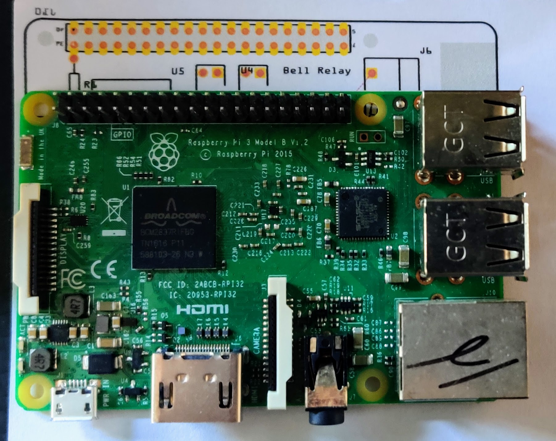
Also I’ve printed it out and I’ve found that actually those slots (not mount points) for the USB and ethernet aren’t as deep as the ones on my actual Pi (3 Model B pictured). But if that’s a hasstle as you say then I’m happy for it to be a board with no cut outs - which makes more space for my circuitry anyway.
Thanks, James.
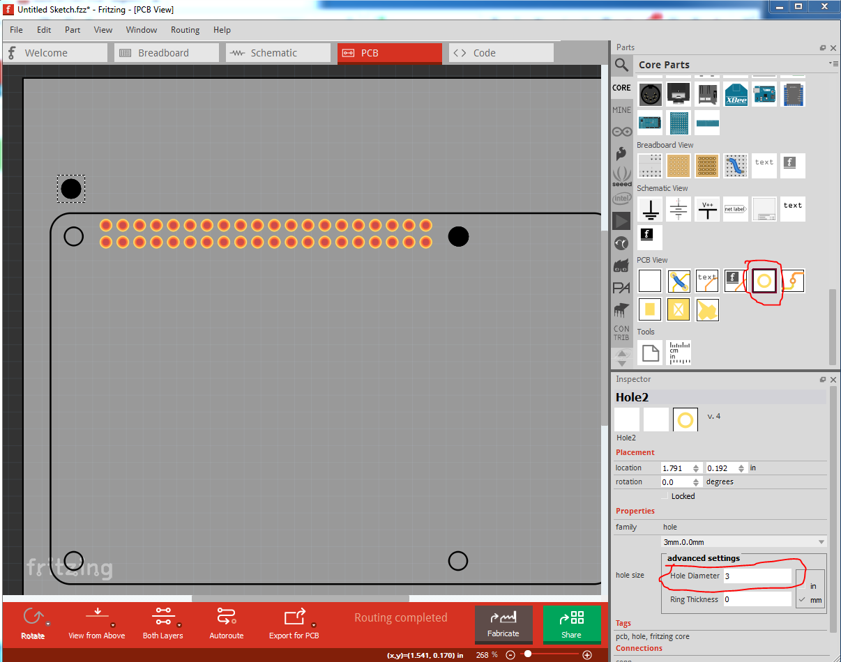
Sure, this is a PI 3 in pcb view. I grab a hole (circled in red on the right side) and View->align to grid unselected so I can move the hole where I like (not on the grid.) I changed the hole diameter from the default 2.3mm to 3mm to match the mounting hole size and dragged it over the hole in silkscreen. This will cause a non plated through hole to be drilled in the pcb. If you want a copper ring increase the ring thickness from 0 (20 thou is the usual value.)
Peter
Thank you very much peter!
I made a hat for Pi3B if you want!
Overlap a Raspberry PI to see if it’s good for you… I upload also the svg if you wanto to make any modifications.
 HAT PI3.fzz (3.7 KB)
Cheers.