A discussion of future direction

This maybe should be in developers but I choose here instead. This is a “put up the flag and see who salutes” type discussion. Below are a bunch of things that I think Fritzing could use (the key point here being I, you may not agree :slight_smile: ).

Parts standards:

The FritzingCheckPart.py script when run against core finds a lot of errors. Considering how (and whether) to try and fix those indicates the need for some further guidelines / standards for parts creation. The Parts file format document on github here:

provided most of the things the script checks for. There are however a few that aren’t covered and probably should be if agreement can be reached.

Below is my list, hopefully you will add yours and/or indicate why mine are a bad idea.

  1. svg file doc height / width in inches, view box at 1px = 1 thou (i.e. height * 100 and width *100) as suggested in the parts file format doc. A Howto article on converting an svg that isn’t compliant in to one that is in Inkscape would be a good thing. It is possible if not exactly easy, and could certainly stand some automation with a python script to make some or all of the needed changes.

  2. schematic connectors .1in or .2in long on .1in centers, part as small as possible for max parts per schematic page and part interoperability (there will likely be exceptions though)

  3. in schematic inputs on the left, outputs on the right (more a guideline than requirement though). For parts such as the Raspberry PI with dual row headers in breadboard the first row of the header on the left of the schematic and the other row on the right of the schematic in the same pin order as breadboard. That is what I am changing all the PI parts to.

  4. schematic terminal 10 thou rectangle as standard, line widths 10 thou for consistancy. This one implies a source change as generic IC and the headers generate 0 width terminals which break Inkscape. So we need to change the parts generator in the source.

  5. breadboard default alignment .1 in (for breadboard compatability) even if the part is smd and thus smaller. In that case mount it on a breakout board with .1 connectors even if there isn’t one available yet.

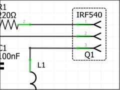
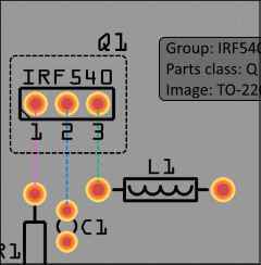
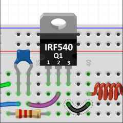
  6. Think about making the part perf board friendly (or two parts, one standard breadboard format, one perfboard friendly where the part only covers the physical space it would take up on the perfboard which may make the connectors in an odd place such as the to220 regulator part here:

    Are top down viewed components available in Fritzing?

    Figure out a new tag for perf board friendly parts so people can find them with search.

  7. Make the parts checking script check for all the cases (it does many of them now, but there are more to add).

  8. Do a clean up of core parts. I have already started on this with the Raspberry PI parts (the Zero which was incorrect, is done and loaded and the rest are in progress as I get time). Focus first on parts that are broken (I’ve fixed three or four some in core for folks that discovered they were wrong) and moveing on from there as time / interest permits. That is part of the drive for parts standards above. We need to know what we are aiming towards when fixing parts.

  9. Once we have come to a consensis (assuming we can :slight_smile: ) get buy in from the parts maintainer since without his agreement this goes nowhere much although the guidelines are still useful.

Now on to a development wishlist:

  1. fix bugs! First and foremost. There are lots of them that could use work and development is starting somewhat and the development environment now works much better.

  2. Change the schematic terminalId size on gererated parts from 0 width to 10thou (assuming proper scaliing). While this is covered in 4 below, this is possible in the short term where 4 likely isn’t.

  3. Figure out a modification to allow us to specify an existing svg in core parts (perhaps core in the svg name in the fzp file). That is a potential big win in that for genric IC for instance there needs to be only one svg for each package size making each part smaller and taking less bandwidth to download it. It also enables a standard footprint library from core in pcb view rather than the current find one where ever you can method.

  4. move the generated parts stuff (variable length ICs, variable length headers) out to a “plug in” type interface that isn’t dependent on source changes to change it (and would allow for local versions for specialized tasks). I’d prefer to do it in python, but we will see whats possible. The idea is to be able make parts that are changeable with inspector without having to change the source and make a release just write and install a plugin to do what you want. We would need to figure out what inspector does internally and how to design this, but I think it should be possible.

There is my current list, feel free to add to it, or disagree :slight_smile: . Also feel free to volunteer to do some of it!

Peter

1 - 4 : I don’t use terminals anymore because I just assign the pin as a terminal and use compass points, but I see how it can force and end to be active.

1 - 6 : Is going to be tough as long a pref/strip borad is in BB view. Pref/strip board needs to move to PCB where parts are already length adjustable and top down.

I would like all of those and even more. i.e. silk always 10 thou, silk alway black, etc

If FZ had an internal parts maker you could force/limit a std more easily, but that is too difficult.

2 - 3 : Even if you optimised FZ svg calls I don’t think it will shrink more than 1%. KiCad is getting massive just from parts - 230MB to 800MB -, and after the initial install most parts won’t be changing.

The major problem is man power, FZ is just too small to get much help, so it’s probably better to just concentrate on the critical stuff like bugs.

I feel that the parts editor needs to be finished so we can stop working with XML files and doing everything manually and instead do it all in the editor. It seems that a lot of what you want is the result of your trying to make things as strict as they had to be before the editor was built. It also appears that the editors purpose it to make parts creation easier by allowing things to be assigned however they are and not have to have everything perfect as you would like. I personally like that you can do things how you want and that you do not have to follow strict guidelines to get a working part.

I personally do not like forced standards as they stifle innovation. If no one had gone against convention we would still be using a rock as our most advanced tool. Allowing people to work the way they are comfortable lets them be the most innovative.

When I make parts I make an SVG of the part with the copper in copper groups and and a silkscreen group, that is all. All other assignment is done in the editor. It takes no time and you never get it wrong. Sure things might look ugly in the XML but if you never look at it who cares what it looks like. 300 groups deep, who cares it still works and I never have to deal with it. It only takes a couple of minutes to make an SVG if you don’t have to worry about making terminals or assigning names to each pad/ring etc. Then it takes only a few seconds to assign the rest with the editor. To make a part completely via SVG and XML it takes much longer and if you have started from an existing part you are likely to have errors. If you start the SVG from scratch it never has strange extra transforms etc. I haven’t had errors making parts since I stopped trying to edit existing parts and started drawing new SVGs. I also keep the original SVGs I create for editing later so I never have to open the Fritzing modified SVGs.

Do note that none of what I have said is in regards to the breadboard as I do not use it and wish it could be turned off when not used to speed up loading and to reduce the risk of errors as it only seems to be possible to corrupt a sketch when using the breadboard and making changes in the other views. If you never work in the breadboard you can make changes between views repeatedly without causing the mysterious extra ratsnests bug.

I know that all of my parts create perfect PCBs and readable schematics. I also know that my parts would fail most if not all of your scripts tests. Does that mean my parts are no good? No. They are all perfect (for me) and work exactly as designed. If you run the part I uploaded MCP1700-xx, SOT-89 through your script you will likely see what I mean. With that all said I think people would rather have as many parts available to them as possible even if they are a little buggy if the other option is nothing making it into core parts because of strict standards. Obviously incorrect foot prints and similar issues that prevent them from being used need to be fixed.

All of the above is my personal opinion and is not intended to make your opinion any less valuable.

This is engineering so I think there should be rules.
I hate adding parts to SCH and finding a simple 8 pin box part bigger than a MEGA2560.
I hate going down 300 groups to fix one little thing.
I hate silks that aren’t black making it hard to do a icon hover to see what it might look like.

Now that I know how to draw in INK you are right about not trying to fix parts but starting from scratch. This is ok for SCH and PCB, but BB is a bit hard.

EDIT

I actually have no problem editing in any view at any time. All I do is picture the part in the other view and what will happen - I will switch view if i don’t remember -, and note the pin #'s and not force what I think is right but use the rats. Sometimes it will leave a rats, but you just check it in other views before you delete it.

This is already being successful, because people are discussing what they would like, which is what I was hoping for. Hopefully more folks will provide input.

The script does fix this one. Anything on the silk layer gets translated to black.

Agreed, if it worked better I might actually use it, so that should be added to the list of things to work on.

Mostly the script is aiming to make parts maintaining easier. If the parts maintainer can run a proposed part against a script it should give a good indication if the part is suitable. Many people appear to be cloning parts (often from core, and getting bad places to start) at least some of them are probably using the parts editor and some are like me ignoring it and editing the xml directly, Having standards that the script will report on doesn’t necessarily mean that parts that don’t conform (at least at the warning level, where there isn’t a known problem that it will cause in fritzing as opposed to Error which does cause a problem of some kind in Fritzing). The choice is with the parts maintainer, but the task is automated more than it is now.

Not really, because while the output is verbose, there is nothing more serious than a warning, and that is only because silk is below the coppers which apparently makes selection difficult. There would be no reason to reject this part (as long as it was run through the script first, as it did remove a bunch of font-size pxs which do break Fritzing and convert the silk from grey to black as it should be). The reference file stuff can be ignored, nothing actually looks at the reference file field except possibly humans as far as I can see.

$ FritzingCheckPart.py part.MCP1700-_819072743e0b360180d372f1c811f2ae_1.fzp
File
‘part.MCP1700-_819072743e0b360180d372f1c811f2ae_1.fzp.bak’

This is a smd part as only the copper1 view is present.
If you wanted a through hole part add the copper0 definition before line 40

Modified 4: File
‘svg.breadboard.MCP1700-_7352f054c1e7d8f2e2ab28ceee875bbd_1_breadboard.svg.bak’
At line 14

ReferenceFile

‘sparkfun-poweric_sot23-3_breadboard.svg’

doesn’t match input file

‘MCP1700-_7352f054c1e7d8f2e2ab28ceee875bbd_1_breadboard.svg’

Corrected

Modified 1: File
‘svg.breadboard.MCP1700-_7352f054c1e7d8f2e2ab28ceee875bbd_1_breadboard.svg.bak’
At line 47

Removed px from font-size leaving 65

Modified 4: File
‘svg.schematic.MCP1700-_7352f054c1e7d8f2e2ab28ceee875bbd_1_schematic.svg.bak’
At line 14

ReferenceFile

‘sparkfun-poweric_lm3480im4_schematic.svg’

doesn’t match input file

‘MCP1700-_7352f054c1e7d8f2e2ab28ceee875bbd_1_schematic.svg’

Corrected

Modified 4: File
‘svg.pcb.MCP1700-_7352f054c1e7d8f2e2ab28ceee875bbd_1_pcb.svg.bak’
At line 5

ReferenceFile

‘sparkfun-poweric_sot23-3_pcb.svg’

doesn’t match input file

‘MCP1700-_7352f054c1e7d8f2e2ab28ceee875bbd_1_pcb.svg’

Corrected

Modified 3: File
‘svg.pcb.MCP1700-_7352f054c1e7d8f2e2ab28ceee875bbd_1_pcb.svg.bak’
At line 14

Silkscreen stroke color #f0f0f0 isn’t white or black. Set to black.

Modified 3: File
‘svg.pcb.MCP1700-_7352f054c1e7d8f2e2ab28ceee875bbd_1_pcb.svg.bak’
At line 15

Silkscreen stroke color #f0f0f0 isn’t white or black. Set to black.

Modified 3: File
‘svg.pcb.MCP1700-_7352f054c1e7d8f2e2ab28ceee875bbd_1_pcb.svg.bak’
At line 16

Silkscreen stroke color #f0f0f0 isn’t white or black. Set to black.

Modified 3: File
‘svg.pcb.MCP1700-_7352f054c1e7d8f2e2ab28ceee875bbd_1_pcb.svg.bak’
At line 17

Silkscreen stroke color #f0f0f0 isn’t white or black. Set to black.

Warning 6: File
‘part.MCP1700-_819072743e0b360180d372f1c811f2ae_1.fzp.bak’
At line 2

ReferenceFile name

‘sparkfun-poweric-lm3480im4-.fzp’

Doesn’t match fzp filename

‘MCP1700-_819072743e0b360180d372f1c811f2ae_1.fzp’

Warning 25: File
‘svg.pcb.MCP1700-_7352f054c1e7d8f2e2ab28ceee875bbd_1_pcb.svg.bak’
At line 13

Silkscreen layer should be above the copper layers for easier selection
in pcb view

This last message (which is why it is last) is the only one that might be worth doing something with. The pxs and style commands have been inlined (and it told you what it changed just in case you care, which you usually don’t) but it is a Warning because it doesn’t break anything, The px does breaks something, but it got corrected. Running the script again (against the corrected output from the first run) gets even less, as it has fixed what it complained about mostly (I need to change the fzp ref file which it currently doesn’t):

$ FritzingCheckPart.py part.MCP1700-_819072743e0b360180d372f1c811f2ae_1.fzp
File
‘part.MCP1700-_819072743e0b360180d372f1c811f2ae_1.fzp.bak’

This is a smd part as only the copper1 view is present.
If you wanted a through hole part add the copper0 definition before line 40

Warning 6: File
‘part.MCP1700-_819072743e0b360180d372f1c811f2ae_1.fzp.bak’
At line 2

ReferenceFile name

‘sparkfun-poweric-lm3480im4-.fzp’

Doesn’t match fzp filename

‘MCP1700-_819072743e0b360180d372f1c811f2ae_1.fzp’

Warning 25: File
‘svg.pcb.MCP1700-_7352f054c1e7d8f2e2ab28ceee875bbd_1_pcb.svg.bak’
At line 64

Silkscreen layer should be above the copper layers for easier selection
in pcb view

So your part is in better shape than you thought (and in even better shape now :slight_smile: at least in this version)

Peter

I am a noob with Fritzing, and this may not be the place for this type of response; but you mention parts and future in one sentence. :wink: Two distinct thoughts from those words:

  1. Fritzing seems touted as an ‘all level’ tool, suitable for beginners and pros. My take after using it for a few projects is that I like it, but it is not as flexible as a professional might like, but mostly is clumsy and above a beginner’s capability for anything but a few stock parts and simple designs. If a beginner needs a part, forget it. I see the whining and complaining all over this forum. Fail. But, if a pro needs a part, he does not want to perform in the circus, even assuming he can take the time to understand how.

I see a lot of people move to other systems due to this. While Fritzing has some awesome features for pros (such as auto ground-fill that is 10 times quicker than KiCAD’s circus) it lacks the easy path to making ‘parts’ that are just to make holes or pads in the right places.

  1. As a separate but related point, I would like to suggest an option for parts ‘grouping’. After quite some thought, most of (my) needs and those I’ve spoken with would be met my dropping holes or pads in the correct position for a part, and then grouping them. Option for a group label. There you have a ‘part’, that can be moved as a group, copied, saved, modified in seconds, or whatever. Very few of us need pin labels (existing ones rarely match), and just the pin number is all we need to match the datasheet for the part. No, it’s not useful for BB view, but other generic parts can be used there, or the group can be overlaid with a black panel and group name for a ‘part’ representation.

Anyway, I am also looking to move-on from Fritzing, and the primary reason is also the parts issue. That’s a shame, and I wish I could do just that little bit more with Fritzing, making it truly a superior small-project tool. Thanks for reading this much. :wave:

While I wasn’t here at the start, I believe Fritzing started out as a tool for beginners. The pros then discovered it filled a need and pushed it forward. If (as it seems) all you want is an eda package then Kicad may be an appropriate answer or geda or one of the commercial products. To me Fritzing’s value add is breadboard (which you don’t appear to want or need). It is the only program I’m aware of that will allow you to document connecting together various modules such as MCUs and sensors to document a one of project cobbled together for something.

Peter

The very first part I grabbed when I started in KiCad was wrong, and that’s when I realised that non engineer people making parts for a free EDA are always a risk, so I went back to FZ. Making a full 3D part in KiCad is probably just as hard as a FZ part because it has a very visual BB view - something that others don’t have -. You either like FZ or not,

@vanepp, @StickyNote, At friends of Fritzing, http://friends.fritzing.org/ it might give you some insight on how Fritzing got started and first funded. Fritzing is an open source educational tool designed to fill in a gap during the beginning of the Arduino revolution. A lot of things have changed since then and I don’t think anyone had any idea how this DIY electronic revolution was going to go…

Some of the fab houses have their own EDAs and of course you have the commercial EDAs. Some of them do pretty neat stuff along with their own learning curve… Fritzing is in a class by it self and shouldn’t be compared with the commercial EDAs. Many of Fritzing parts are provided by people like you and me and usually not tested for errors. But I believe Fritzing still does exactly what it was designed to do; and that is to take the student from learning how to read and draw a schematic, test it out on the breadboard, and then design and build a PCB prototype. Like any new program has its own learning curve, it takes awhile to get the hang of it. Fritzing is a lot easier then some of the EDAs… you just got to learn the little tricks… There are things you can do with Fritzing that you can’t do with the commercial EDAs.

I think the most difficult thing about Fritzing is getting Inkscape down to a science. Inkscape has a lot of settings and if they are not setup right, your .svg file does some strange things when imported into Fritzing, “like your scaling problem or strange through hole sizes…”. One of these day, Fritzing will have its own graphics program for creating the .svg files for parts which will make things a lot easier to edit or create new parts.

2 Likes

I have read that, I just wasn’t involved in Fritzing at that time so am not all that knowledgable on the history involved. I can clearly see the results though :slight_smile: , the underlying design of Fritzing is awesome and very well thought out.

I’m hoping my parts checking script (unfortunatly along with a lot of work) will help correct that. I’m working on cleaning up the Raspberry PI family (the zero is already done as it was broken) and will branch out from there, with priority to broken parts (with pauses to fix the script as it breaks :slight_smile: ). That’s why I started this thread as what I want may not be what the community wants or needs.

Even worse is that the two of them have different (and not very compatible goals: Fritzing want’s the svg tiny subset and Inkscape wants to be CSS compliant which Fritizing doesn’t fully support. Neither is wrong, their goals are just different. Again my python script is partly designed to fix that. It takes the output from Inkscape and modifies the parts of CSS that Fritzing doesn’t support in to equivalent xml (I hope) for Fritzing (current inlining style commands and removing the px from font-size commands). Ideally the script would move in to the Fritzing load routines to occur automatically on load, but that is a future. I’d like to see the script remain external to Fritzing (just called from load) so the script can change to track Inkscape changes without having to do a new release of Fritzing but we will see.

Hopefully that will become true, although I suspect breadboard is mostly still going to need an svg editor for many types of parts, but for it to happen we need to get people developing. There is light at the end of that tunnel though, the development environment is now working again and I (and I hope others) are working on fixing some of the bugs. I have a fix for the segfault and hang caused by a corrupted part submitted as a pull request and am working of figuring out how to get parts editor to delete the files it creates in the mine parts bin when it makes a part (this is considerably more exciting to do than the first fix). If we can come up to speed on the code base we may be able to start working on parts editor. There is a todo list in the source that describes some of what they thought should be done next.

Peter

I think the guy wasn’t interested in finding out what happened - or he would’ve supplied the .fzz -, he just wanted someone to blame. The drill.txt showed 3.1, 3.8, alternating holes, so if the PCB came back with 3.8, continious it wasn’t FZ’s fault.

The part checking script is good, but it still leaves the problem of miss labeled parts, i.e. a 3.5mm screw terminal that is actually a 3.81mm.

BB view is very useful, and my suggestion incorporates that. I may not use it as much as you, but it’s still there! I am a results-oriented person, and I tend to favor the simplest and easiest path to arriving at desired results. To this end; by suggestion was to simplify the parts process into a simple modular “group” of elements to serve the same purposes as the current parts and editing, without locking into a zillion parts that only serve one function. Here is a quick example of what I mean:

Let’s say we want to incorporate an IRF540, and there is no part. Easy. In schem-view, drag out some pins, and “group” (function) the pins and attributes (Goup Name: IRF540, Part Class: Q, Pin Numbers: 1,2,3, Image: TO-220, etc.) It looks like this in schematic view:
Schem-group

And connects like this in PCB view:
PCB-group

And appears like this in bread-board view:
BB-group
A handful of generic images including standard transistor types, adapter boards (non-specific like they are now, which all look the same but are repeated for each different part), resistors, and so on. Instant parts, without megs on megs of individual and difficult-to-edit parts, and always without the exact one you need. I’m sure there is a more logical or sexier way to represent them, but it’s a quick example of concept. Is this too simple? What am I overlooking? Thanks for your input.

1 Like

I know what you mean, and you can do something similar by locating vias off the PCB and group moving them in, it’s just that all EDAs use a complete footprint for a part so that method seams like a patch for the more common way.

When I started I had trouble with the complexity of svg drawing - it’s nothing like raster GIMP - so I used every method to skirt around actually learning how to draw in INK - I imported pdf drawings -, but once I learnt to draw parts, which isn’t that hard, I find it a snap to just do the correct footprint and import it into a new part.

I made a tutorial video series that teaches you both FZ part making and INK drawing all in one hit, and that 90min will save you 10’s of hours fumbling around.

KiCad has more features, but the clunky way you have to use it is like going back to the stone age - it’s a lot of separate programs under one wrapper that don’t talk to each other -. You select parts for the SCH, layout the circuit, export the parts from SCH, import into PCB, pick footprints for the parts - SCH and PCB drawing are not joined -, and lay them out again. And I think if you change something in PCB you have to also do it in SCH, because the views aren’t connected. I suppose you get used to it - you have to learn a lot of short-cuts -, and it has some cool stuff, but simple things like a junction you have to grab like a part, where’s FZ you right-click or pull a trace. When I started 2 years ago I trialled FZ, Eagle, and KC after watch hours of tutorials - it’s the only way to learn them quick - and I liked FZ, maybe you’ll like something else.

I think what you are suggesting is already present in the mystery part. Where it falls down is when you need a custom footprint. I expect as @steelgoose said earlier the correct answer is to finish the parts editor (which is currently not finished). To do that we need to get people willing to put time in to development which currently isn’t happening (or at least not happening enough).

Peter

Thanks for listening, and I wanted to assure you this is not hypothetical. What I described above is actually what I do with Fritzing every day, as my process improvement workaround. My frustration is not having the simple “group” function in order to manipulate the blocks easily for moving, flipping, etc. and assigning an image. With these abilities, grouping becomes a very powerful and easy-interface tool.

I understand Fritzing was not intended to be an EDA, and in that vein, should not necessarily be tied to traditional EDA methods and their limitations. I don’t want to move-on from Fritzing. These minimal functions would empower it so I would not have need to, and I feel helpless as I have no coding ability to help in attaining it. Thanks all, for what you do for Fritzing.

I think this is likely the problem, the group function isn’t simple internally. The code is set up to deal with parts as svg files (not groups of svg files as your group function would need) so you would need something capable of combining several svg files in to one i.e. the missing svg editor in parts editor. I’m having an exciting time trying to figure out enough of how the code works to fix some of the bugs I know about (at the moment related to saving and deleting parts) where the code already knows how to do what I need somewhere else but not in the place that I want it. It is difficult to follow the flow of code to isolate how it eventually deletes the files which is a relatively simple task. Manipulating svgs is going to be much more difficult (although again, the code currently does it). So basically I wouldn’t hold my breath. Unless we can attract some of the original developers back to provide at least guidance and suggestions of how things should be done, improvements (even as simple as bug fixing) are going to take a lot of time.

Peter

Out of curiosity, how far from a Release Candidate or another Beta was ver 0.93b?

Assuming “was” above should be “is”, it is hard to say. The new gerber code (which is the biggest change) has been backed off as not working. The development environment is now building correctly (it didn’t used to). It has been said if we get a reasonable stable build, that they are agreeable to doing a new release but without the gerber code I don’t currently see enough fixes to make a release worthwhile. I’m working on fixing some of the file type bugs in case there is a new release , but its going slowly. So I’d guess it isn’t going to be soon but I don’t really know. Getting a stable buildable head is a good start though.

Peter

I don’t know if this belongs here but if you’re talking about future features I believe the parts bin needs a radical rethink.

It must have worked as a POC with a very short component list but I’m finding it very hard to navigate now and surely it will get worse if ranges of ICs are added.

Sure, we are discussing future directions and volume isn’t so far a problem :slight_smile: getting people willing to do the work is though . While I agree both parts bin and search need work (search is even worse than parts bin in my view) it is well down my list after learning the source to fix bugs and add new features, doing more work on the parts check script and fixing up existing parts. That said, of the two parts bin is easier because non core parts are user changeable (search is possibly a code change or possibly better tags in individual parts either of which are more complex). You can move things around in the parts bins and create new bins for your self with the current code with no code changes needed. If you (or any one else reading) would like to help, that would be an easy place to start. Move stuff around in the bins and add new bins to better arrange the bins and post what does and doesn’t work for you (including what code changes would improve the situation but realizing implementing is likely to take a long time). For core parts, once you have a better arrangement (which you can demonstrate by copying the part in to the mine parts bin then moving it where you want) that can be done by submitting a change to the parts repro on github which is also much easier and more timely than a code change.

Peter