The check script has a number of thing to complain about in the first part (I didn’t check the rest): There are px on the font-size entries in the xml which will cause the fonts to become 0 size (and thus disappear) if you edit the part (the script automatically corrects these, so it just notes it has, it isn’t an error). There are blank lines in the xml (which it complains about because they are unusual) but that won’t break anything. Then it complains about pads with no radius because you have copper0 in an SMD part. SMD parts should only have copper1 no copper0 as they are only on one side of the board.
I’ve explained this before. If you do not have both layers it will only work on one side and when you try putting it on the other side it will appear there but it will actually be reversed and useless.
Not a fan of copper pads floating around on the underside of a PCB, plus not many people double load, so I would prefer just copper1. If I needed and underside part I would just swap the copper1 for copper0 in the svg and make another part.
How did you do that? I would guess that you edited some through hole part that makes Fritzing think this is supposed to be on both sides at the same time. I only work with SMD parts (with the exception of headers and wires and Nixie tubes) and have made hundreds of parts for myself and I always have both layers. I only have the paths in the one group which is inside the other group. If you only have the one layer like you and Peter suggested then you will only be able to use the part on one side which is useless unless you only make single sided boards or label all your parts as being top or bottom or open each SVG before using a part to make sure it is for the side you are using.
@Old_Grey Please upload the part you made that does that to see why you are getting it wrong and so I can explain again how to do this so you guys stop giving the wrong advise. Actually the advice on parts creation being given is one of the reasons I have stopped helping as often. I am tired of explaining how things are done using the new editor after someone else has explained how things were done at the beginning of Fritzing before the editor and trying to force rules on people that make ZERO difference in a parts usefulness while making parts creation seem way way harder than it actually is. If you use the editor and ignore 99% of the rules required for the old parts creation then parts creation for everything except the breadboard is really really easy. Most parts can be made in under 10 minutes even if it has lots of pads. I NEVER EVER have to edit the fzp files or do any work with a text editor. You simply create the svg without all the extra elements and tags and then use the editor to assign things. It will create a part that by the old antiquated standards has issues but by the new undocumented standards used by the editor it is perfect and takes no time.
Here is a random proper SMD part I created and it has both layers and works on both sides as it is supposed to. MAX6920.fzpz (9.8 KB)
Sorry for the rant but as you can see I get frustrated reading old overly complicated instructions that make peoples lives harder for no reason.
I used the posters part because I thought you were saying that it was correct having both coppers. Now I see you reversed the groups to blank the bottom layer.
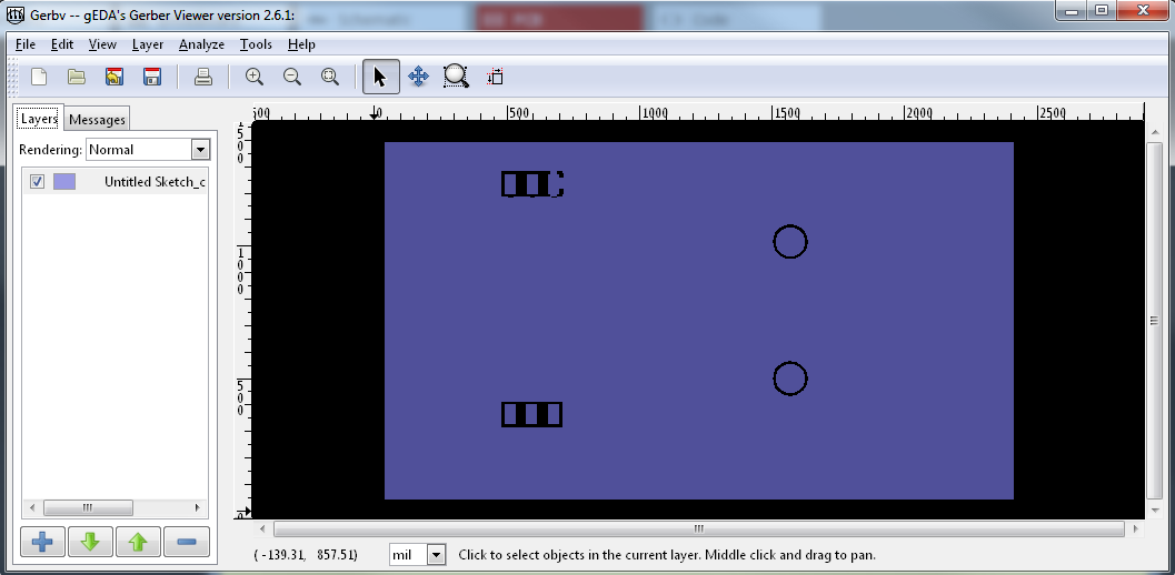
While we may yet agree to disagree, I’m all for trying to fix any frustration that keeps you from replying here. That said, I saw the post that you referred to above and I (in a fairly quick read) don’t understand the problem. I also don’t understand the issue why a copper1 only part doesn’t work, because it seems to for me. Take this pcb screen shot:
which contains the poster’s original part (on the right, which I maintain is wrong), a modified version with only copper1 (on the left, which I don’t see anything wrong with, although there may be) and your example part which while more correct still allows invalid connections (pin2 on the bottom layer) which I would maintain is wrong if workable if you are careful, but is bad for beginners in that it allows them to do something incorrect without complaining. If the single layer version isn’t working, then we have a bug that we should work on fixing. Referring to the pcb image above (which matches what gerbv sees from the gerber output, the original part is incorrect because it 1) has pads on the bottom layer and the top which will interfere with other smd parts on the opposite layer, and 2) allows connections on both layers which simply won’t work. Your part has pads on only one layer but will allow you to move the trace on pin 2 to the bottom layer when the part is on the top (hmmm, something wrong here, when I reloaded the sketch, it is complaining about missing files so the fzz may be incorrect in some way.) however it is declaring routing complete which is incorrect because it isn’t. Now on to why the single layer version is wrong (which I’m not seeing). I added an extra pad (with no connection) as the original is symmetrical except in silkscreen (I just realized I should have added a second pad in case the problem is in vertical instead of horizontal positioning). I then did one on top of the board and one on the bottom, and as far as I can see they are positioned correctly and should work fine. It won’t allow me to move traces between layers (because that is wrong). So what am I missing? If there is a bug, I need to understand how to recreate it. With the lack of documentation (and the fact that I wasn’t involved in Fritzing when development was still going on) I’m not sure about this, but I think that copper0/copper1 is a new feature in 9.3.b, I don’t think it was there in earlier versions so I don’t think it is an old no longer used concept (although it may have bugs). The folks that designed Fritzing appear to me to have been looking far ahead in relation to how new things should work and I’m not inclined to violate that without a real good reason.
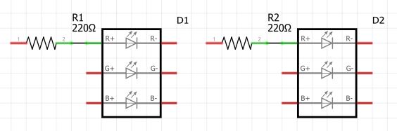
Unfortunately your connections to the MAX are red, hence not connected.
Saying that people don’t listen works both ways, because you(Van) has mentioned on numerous occasions that you don’t actually USE FZ much for making circuits. So a quick person would realise that you do not see the resultants of stuff like this on a daily basis, so are not going to intimately know what happens.
I just don’t see the point of the huge flame post when he could’ve said, “keep the 2 groups, just reverse the copper labels.”
You are the person here everyday making parts for people, so being flamed for one mistake, ie not remembering a 1 year old post, is rude. You can say what you want in a reply, but remember to respect people trying, because no one else is.
So we learnt something today, no need to have a hissy-fit.
You are correct, I had missed that. It is in fact a double error in that I was lazy and didn’t make the connections in schematic, which is why routing was showing as complete so that part of the original post is also incorrect. It appears I routed the wires on the top (with the chip on the top) then moved the chip to the bottom layer and then clicked on the wire (which isn’t connected to anything) and moved it to the top layer which Fritzing doesn’t see any reason not to do (although I think it probably should)…
I’m not all that concerned with the tone of the post but with the frustration that is causing him to post less and in understanding if there are bugs, how to reproduce them. It looks to me like there are perhaps some bugs present here and I’d like to understand what they are. I’m still interested in why the single copper layer part is thought to malfunction, because it doesn’t seem to be doing so to me, but as you said I rarely make boards and may be missing something.
I for one am sorry to see you go and hope you will reconsider. You provide much needed expertise on pcb related issues that I (and most anyone else still posting in here) don’t have and that is a big loss.
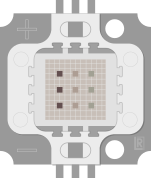
The thing I find annoying is the FZ error that you are missing a copper layer, and if sub’s method works, it is a good one. I tested the LED part because I thought it was correct, because I wanted to see how it was done. But when I saw the bottom layer with pads, I thought it wasn’t a good idea. Now that I see a proper part, it is a good idea, it’s just that we didn’t know about it at the time.
I’m not that into FZ anymore to experiment, but if you(Van) do some tests to test it, it might be a good thing to add to the script.
Tracking back the referenced post I found an earlier one that it looks like I forgot about that suggests there is a problem with non symmetrical pads. I’ll poke at that and see.
I’m not surprised , until a few minutes ago I was mostly confused about what the issue is as well. It doesn’t affect this part I don’t think, only ones with non symmetrical pads (and I need to test that to be sure). So it seems to be an odd corner case (I haven’t run in to an SMD footprint with non symmetrical pads yet, but I don’t do much with SMD either) with a proposed solution (if that doesn’t cause some other problem) that may be worth adopting.
When I grabbed the 1st LED I GND filled the PCB, and when I looked at the bottom it had floating pads. I grabbed sub’d MAX and it didn’t. I took a quick look at the svgs and the LED had the copper#'s in reverse order than sub’s, so I assumed it’s that. If it’s not I’ll have to leave it to you guys to figure out why.
Well, cancel that last comment of mine. I’m still confused. In the post about titos copper artwork the ‘universal works both sides part’ is a standard SMD part with only copper1 defined, no copper0 in copper1 in evidence in either the svg or fzp files. There is a property called true which I’ve never noticed before but that’s it. Since the original files appear to have been edited over I don’t image I’m ever going to figure this one out … Removing that property doesn’t appear to make any difference so I’m at a loss as to what the issue here is and how it was fixed other than it doesn’t appear to have anything to do with copper0 and copper1.
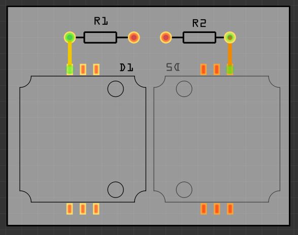
Damn, you’re right. I swapped the copper# in the LED and it shows the pads on the bottom, but sub’s doesn’t.
Holy moly, you can move the Copper Fills in a sketch.
I swapped the copper# in the LED svg and made another part, and this is what I get.
Top layer left, bottom right. Un-moded LED left, my reverse copper right.
No, as I said there isn’t enough information there (in terms of the file that was started from) to tell what happened from beginning to end. Unless someone comes up with another case I don’t think we are going to figure out what happened. It does not appear to be related to copper1 / copper0 from the end result but other than that I don’t know.