Mid-Mount SMD Part Creation

If you post the part .fzpz file I’ll have a look. The most likely answer is translates, they tend to react badly (sometimes) in gerber creation and are evil in general as they are likely a performance hit as well (they require a matrix multiplication to render). They are somewhat difficult to remove sometimes (ungrouping and regrouping will remove some of them though).

Peter

vanepp, the part that I got from you (Generic female header - 23 pins-1.fzpz) has the same problem.

That is odd because it appears to work for me:

although when I look at the gerber output in detail the pad internal spacing is probably not large enough (from the gerbv gerber viewer):

Perhaps I was wrong about being able to not remove the transforms. I’ll remove them and see if things improve, although neither of these are as bad as you example.

edit:

Not the translates (although I removed them anyway) but something in the extra stroke xml. Stroke is set to none so that shouldn’t impact anything but setting stroke-width to 0 and linecap from round to butt corrects the gerber spacing (most likely the stroke-width, with gerber ignoring the stroke=none parameter).

Generic female header - 23 pins-2.fzpz (8.0 KB)

Is the image with the bars all merged by chance an svg of both layers of the board? The Inkscape pcb svg looks like that because both copper0 and copper1 are overlayed and you have to delete one or the other layer to see the real spacing of the pads.

Peter

Awesome, setting the stroke width to 0 and cap to butt in inkscape worked great!

New problem! When exporting the file as Gerber it neglects to include part of the contour. Any ideas?

Good progress!

Regarding “New Problem”… From my experiences with similar problems:

• These truly do affect the outcome:

  • the aspects of making lines
  • closeness to other lines and cutouts
  • radius’d corners
  • difference/subtraction order and path
  • layer order in the file

I recommend first verifying the missing cutout is in the correct layer and was attended to with respect to the above and my previous comments.

Second, make it a rectangle (no radius corners) and see what happens

If you post your PCB file I’ll look at it

Check the missing element for translates or other changes from the ones that work. As always post the sketch and we will have a look, it is hard to say without looking at the xml and/or experimenting with the part.

Peter

As mentioned above, “radius’d corners” will affect outcome. Took a few moments as I wanted to post this followup to underscore that point… (mostly for future readers of this post).

Attached result shows the same file with only difference in the ‘corner’ of the rectangle: one with Radius, the other Without Radius.

The Contour file shows one with Radius’d corners simply would not properly work in Fritzing (though the SVG is good). No matter how I Path’d, Differenced, Subtracted, Grouped, Filled… etc

Could you upload the files for these two please? I’d like to figure out how to make slots and to try and figure out why it fails because with development starting again we may be able to fix it.

Peter

files attached.

Note: Sometimes the radius corners will cause only the specific shape to be missing.
Sometimes all of the cutouts will be missing. Somewhat non-consistent and can depend on size of radius, stroke…etc

NotWork.fzz (29.0 KB)
Works.fzz (28.9 KB)
NotWork.svg.fzp (128.1 KB)
Works.svg.fzp (127.8 KB)

making it easier… I deleted the unnecessary items.

These have only a silk perimeter and the cutout…

simplified_woRadius.svg.fzp (1.1 KB)
simplified.svg.fzp (1.4 KB)

Thanks, I’ll have a look and see if I can figure anything out.

Peter

The simplified files would be easier to inspect as they eliminate the bazillion data points created by Pathing the text, face image… etc…

I think we have more than one problem here. It looks like Fritizng is assuming px as dimensions (which is a problem because that depends on what it thinks a px is 72dpi, 90dpi (I think what it is using) or the current 96dpi (which I don’t think it knows about). This gerber image from the working svg (in orange) is dimensioned in px. The purple one has only the units changed from px to in, which should only change the viewbox, but as we see it also changes the scale and causes truncation. I suspect this is why you need to use a path on the text, Fritzing is getting the scale incorrect when it renders standard text (which is why I was trying to get dimensions in inches). There is also a transform in the silkscreen Perimeter_Rectangle which may or may not be causing problems (it shouldn’t affect the board layer cutouts though they don’t have any transforms). I need to figure out how to create one of these things from scratch to see if starting out with a drawing in inches at the standard scale makes any difference (its possible the paths are not being scaled when the units change for some reason) but so far I haven’t figured out how to get the path difference to work.

Peter

I wish I knew better what was going on but this is what I did

  1. Open board outline in Inkscape
  2. Create rectangle that is just a fraction bigger then the original hole/cutout
  3. Difference rectangle (with radius’d corners) from bourdoutline
    a. Select both shapes
    b. Ensure the rectangle is on top
    c. Select Path>Difference
  4. Export as Plain SVG
  5. Voila, the gerber looks correct

Oh course the downside is now the hole is a fraction bigger, not big enough to make much of a difference I wager.

image

Could you post the .fzpz files from both the one that doesn’t work and the one that does please? I’d like to see what the difference in the xml is to maybe figure out what is going on.

Peter

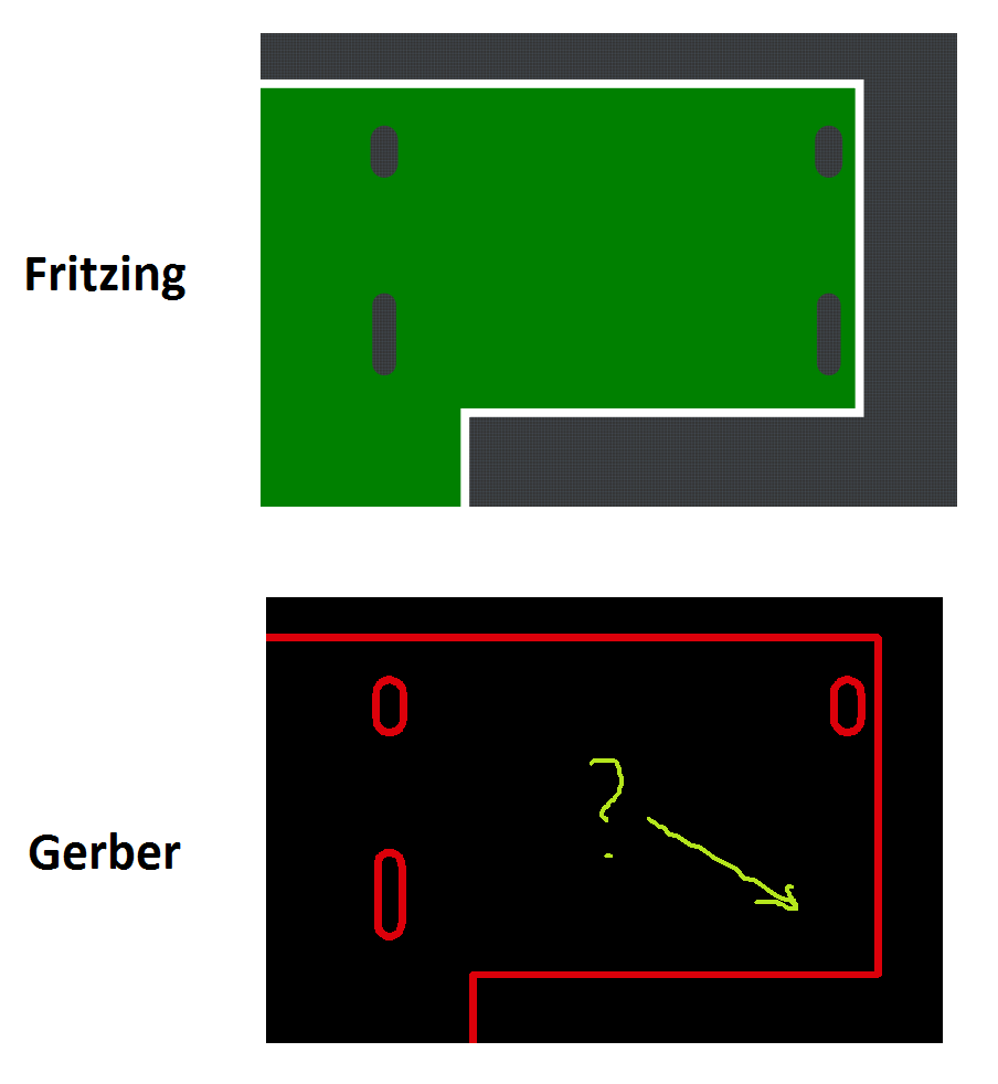
Because I make my PCB’s via CNC milling, which always points out the problems with cutouts, I spent many hours trying to figure out work-arounds.

Thus, that is why I stated my comments in above posts - e.g., size, proximity, etc, etc, etc… and that “you can get there with a bit of work”

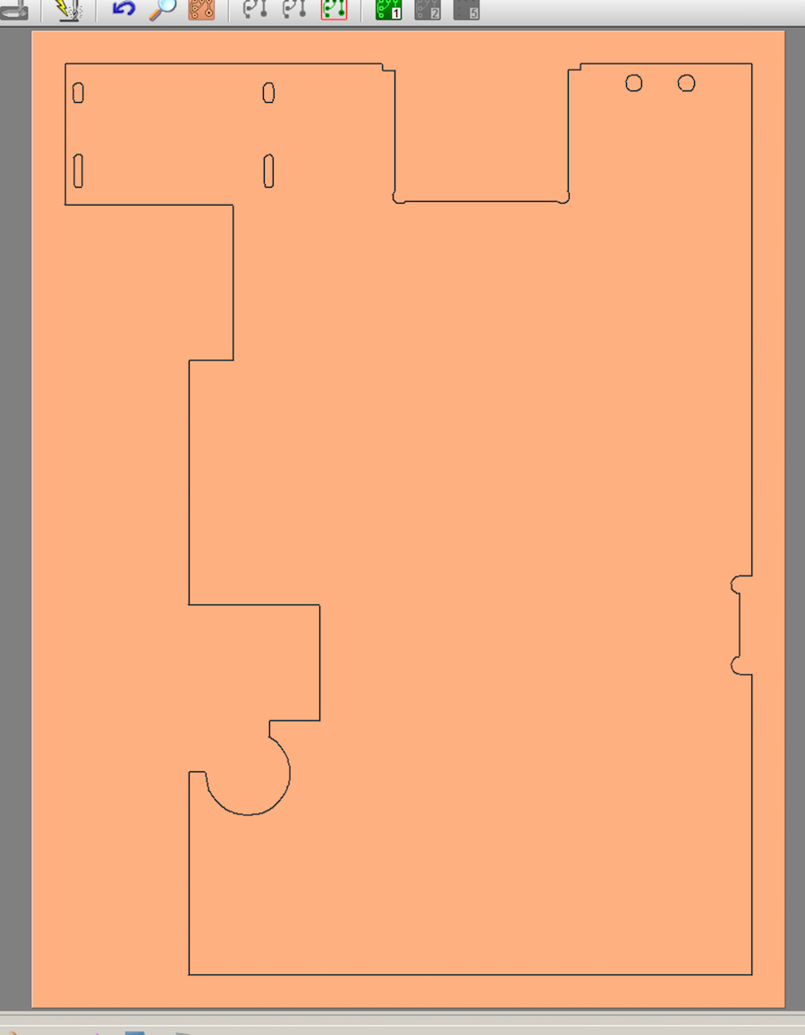
To help (Peter’s) investigation, the following two additional files are attached along with images of svg data:

These two attached files are minimal, containing:
Empty Silkscreen layer
Board layer with Rectangles (for board and cutout), and Differenced the two rectangles (thus resulting in a Path)

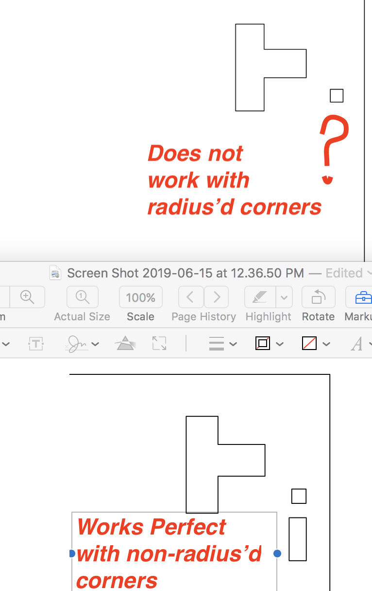
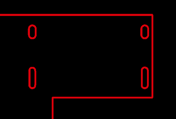
One file has 90º corners
One file has Radius’d corners

Both drawn in Pixel units (78.8px)

Thus, only difference in ‘Designed’ SVG’s are the data points regarding the corners. Units are undefined, thus assumed to be px.

I’m thinking, regardless of Units, whether specifically defined (px, mm, inch) or not, the only logical resulting difference should be the size, if units is the issue.

Fritzing loads both files with result of 22.2mm

After loading, I exported both of them from Fritzing as SVG images. The results show both with the same Correct Inch dim’s. Other differences appear to be non-consequential.

Rect_wRadius.svg.fzp (733 Bytes)
Rect_woRadius.svg.fzp (566 Bytes)

I was curious, as follows:

Wondered what Fritzing would do with homemade SVG containing only drawn elements, No Layers.

I hand-coded some svg elements, did not Paragraph them nor made any attempt to ‘pretty it up’ or do anything beyond drawing the elements.

I loaded it in Fritzing for a PCB image and it loaded just fine. All elements correct, including Radius’d corners. The exported Gerber uses the last drawn element for the contour (as I did not Path, Differenced, Subtracted anything). Thus, it did what I expected it to do (if it indeed would load).

FYI - You’ll wonder why the big black triangle? That was an element made as a Path. It only shows in the PCB view but not in exported Gerber. I deleted it in the attached file…

myTest_1_svg.svg.fzp (1.3 KB)

Sorry for the delay. Here are the two Fritzing Projects.
WorkingGerberExport.fzz (3.1 KB)
NotWorkingGerberExport.fzz (2.8 KB)

Looks like you’ve gained a good understanding of ‘how’ to do it.

The “NotWorkingGerberExport” shows two elements on top of one-another (image below).

You didn’t post the SVG so, no comment other than to check it out and see what&why…

[EDIT] Added image of the Laser Cut board from the WorkingGerber. Note: Flipped Horizontally for laser cutting… Used 0.1mm Kerf (width of cutting beam)