XY-SP5W 5128 - 5W Mono Audio Amplifier Module Class D Digital

Product Name: XY-SP5W 5128 is a 5W Mono Audio Amplifier Module, Class D Digital - 2.5-5.5V DC - Low Distortion.

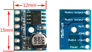
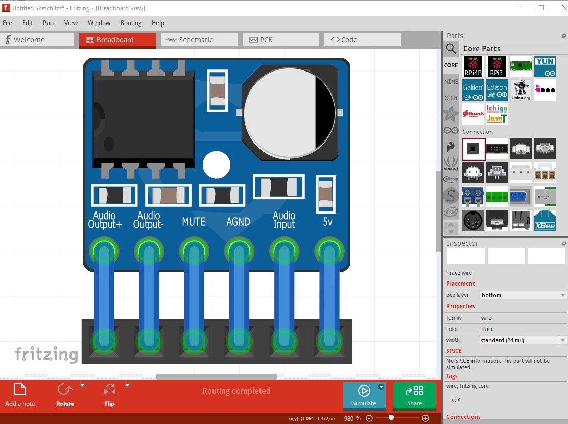
Description: The mono power amplifier module uses the LTK5128 class AB/D power amplifier IC, featuring low EMI and low quiescent current, no external low-pass filter, and efficiency up to 90% in D-type power amplifier mode. The LTK5128’s unique DRC (Dynamic Range Control) correction circuit technology reduces distortion caused by waveform clipping when high power output is reduced. Compared to similar products, the dynamic response is better. It includes short-circuit current protection, undervoltage protection, and overheat protection.

Download:

XY-SP5W 5128 - 5W Mono Audio Amplifier Module Class D Digital.fzpz (11,7,KB)

Manufacturer: Hunan Hualai Technology Co., Ltd.
Part / Module name: XY-SP5W 5128 Digital Amplifier Board (5W Class D)

Your part likely has scaling issues as the svgs are dimensioned in px,

Warning 19: File
‘svg.schematic.XY-SP5W 5128_1deb0f85b717b891bf3971a5d3e96a74_2_schematic.svg.bak’
At line 3

Height 79.92 is defined in px
in or mm is a better option (px can cause scaling problems!)

Warning 19: File
‘svg.schematic.XY-SP5W 5128_1deb0f85b717b891bf3971a5d3e96a74_2_schematic.svg.bak’
At line 3

Width 83.146 is defined in px
in or mm is a better option (px can cause scaling problems!)

Warning 19: File
‘svg.pcb.XY-SP5W 5128_1deb0f85b717b891bf3971a5d3e96a74_2_pcb.svg.bak’
At line 2

Height 34 is defined in px
in or mm is a better option (px can cause scaling problems!)

Warning 19: File
‘svg.pcb.XY-SP5W 5128_1deb0f85b717b891bf3971a5d3e96a74_2_pcb.svg.bak’
At line 2

Width 42.5 is defined in px
in or mm is a better option (px can, and in this case is, cause scaling problems!)

The schematic svg displayed in Inkscape is not on 0.1in boundaries which it should be and is dimensioned in px which should be in or mm.

which causes the pins to not be on 0.1in boundaries which they should be.

and thus causes misalignment in schematic in Fritzing.

FritzingCheckPart.py (which generated the warning messages) and how to fix this is available in this part making tutorial.

Peter

Hi Peter, I made the corrections you showed me. Can you check the file?

Download

XY-SP5W 5128 - 5W Mono Audio Amplifier Module Class D Digital.fzpz (11,5,KB)

Better but still a problem in schematic. The pins should be aligned to the 0.1in grid but are not.

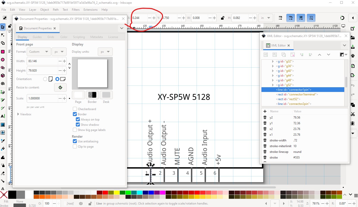
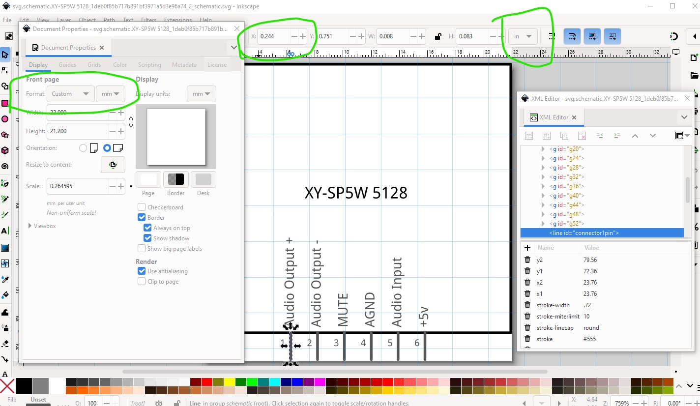
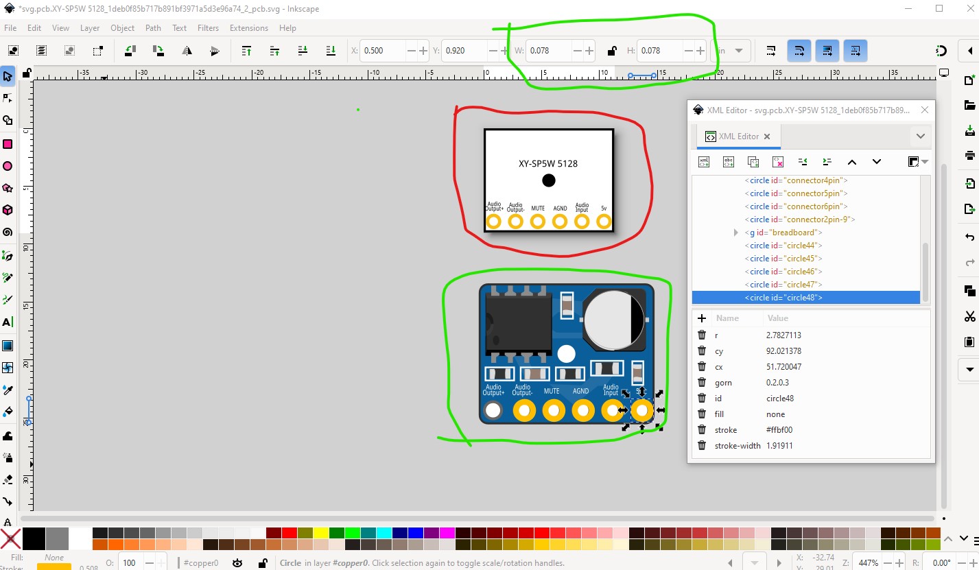
If you are using Inkscape as your svg editor Randy’s schematic extension is the easiest way to get a correct schematic svg. Manually you just need to move the pins to be exactly 0.1in apart

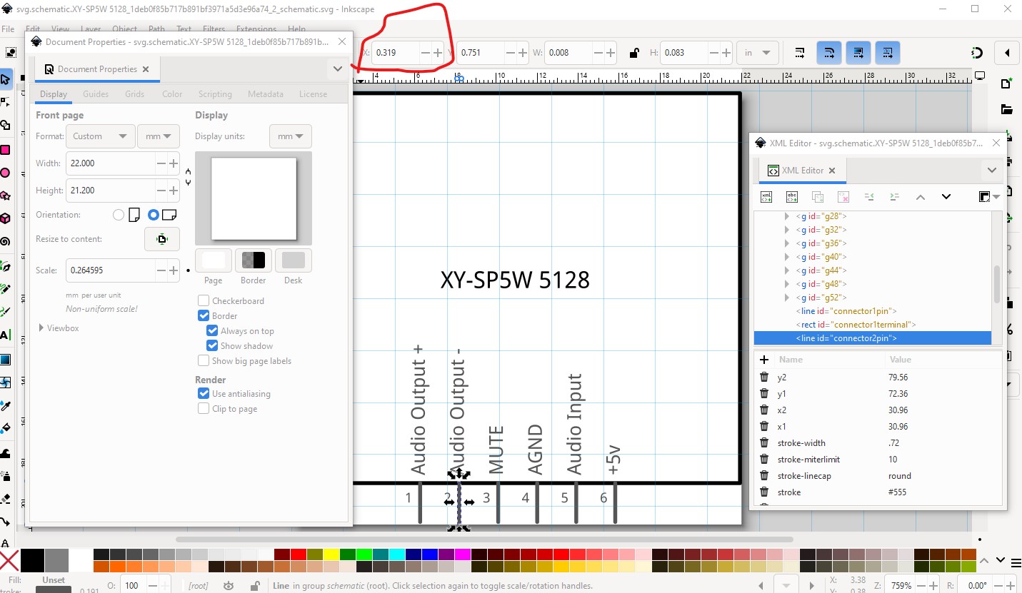
Since the first pins is at 0.244in, the second pins should be 0.344in not 0.319in as it is at present. Just selecting the entire pin and setting them exactly 0.1in apart should fix it fairly easily. FritzingCheckPart.py doesn’t flag this as an error as it doesn’t check the pin spacing.

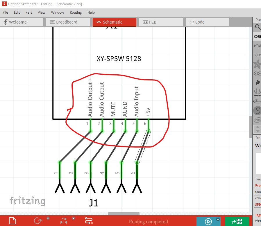
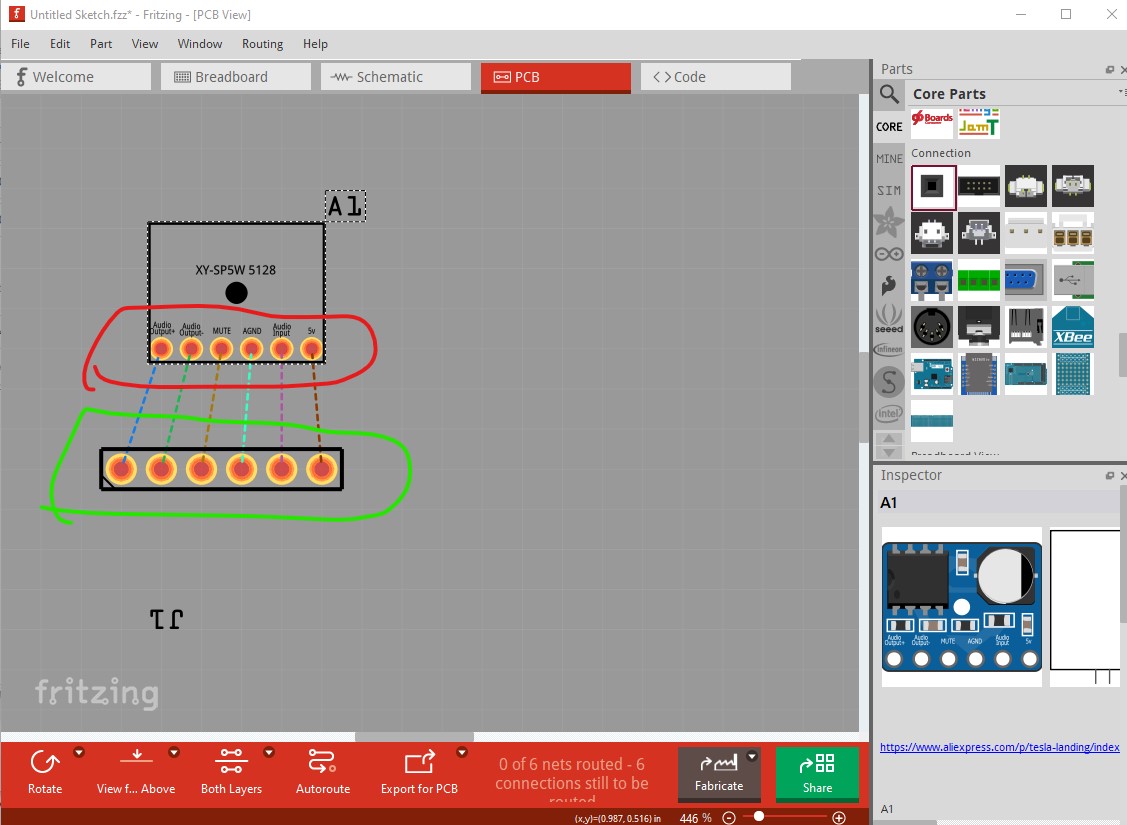
Same thing in pcb, the pins are most likely on 0.1in centers but as we see from the header (which is the correct 0.1in pitch) your pcb is not and thus won’t fit.

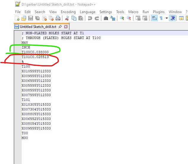
As well the holes are too small. Here I exported the sketch to gerbers and then edited the drill.txt file to get the hole sizes. The headers should be 0.038in but yours are 0.028 (probably because the pads are the wrong diameter because of the scaling) which likely won’t work.

Parts making is a complex process which tends to bite without warning! Hope this helps some.

Peter

Ok! Now i think it’s correct! Peter, can you check again?

XY-SP5W 5128 - 5W Mono Audio Amplifier Module Class D Digital.fzpz (11,5,KB)

Breadboard and schematic are good, pcb still has problems.

Pcb is the wrong scale and doesn’t match breadboard (which it should!)

Here (in Inkscape) I copied a correctly sized header pin (the gold circles) and the breadboard svg which matches the correct scale for the pads. As we see the current pcb svg is scaled too small. I often just copy the breadboard svg in to pcb, delete all the uneeded stuff and set the base of breadboard to fill:none stroke: #000000 and stroke-width: 10 as the outline and then place the correct pads

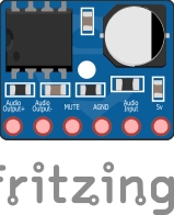
I will upload the actual svg displayed above so you can look at it (right click on the image below and do a save image as to download it.)

svg.pcb.XY-SP5W 5128_1deb0f85b717b891bf3971a5d3e96a74_3_pcb

On the left I duplicated the board from breadboard and changed the stroke and fill values to what pcb wants to form the proper outline for silkscreen. The gold circles in the breadboard image should produce the correct 0.038in holes in the gerber output.

Peter

Hi Peter! Can you check again?

XY-SP5W 5128 - 5W Mono Audio Amplifier Module Class D Digital_Updated.fzpz (12,1,KB)

Looks good! Exports to gerbers correctly with the hole size being 0.038in and the traces lining up with the header so it should now be fine.

Peter

1 Like