OK here is a part and how it was made. Most of the stuff is in this tutorial on making parts.
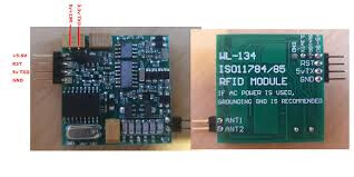
Started with your svg above. Grabbed a jpeg of the board from this site
https://www.ebay.ca/itm/153965483456
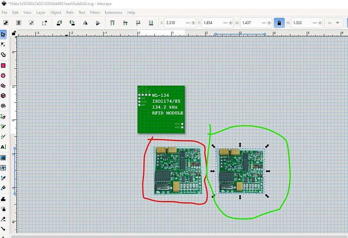
which is slightly rotated and warped. Imported the jpeg in to Inkscape and rotated it and then used the Raster perspective extension to convert it to a flat image like this (original in red converted in green)
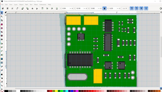
then scaled the result to match your svg image
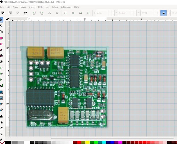
which gives me the placement of components on the board. Then pasted the various components in to the svg overlaying the components on the image.
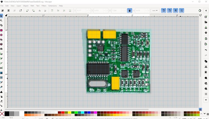
at the end of that breadboard looks like this (with the image at the back)
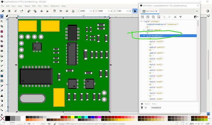
then I deleted the jpeg image, ungrouped the svg reset its viewbox and grouped the result and named it breadboard to set the layerId.
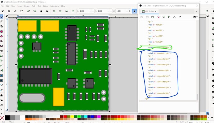
The connectors are grouped at the bottom of the svg (which allows me to automatically renumber them with a script which I did here.)
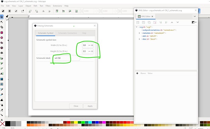
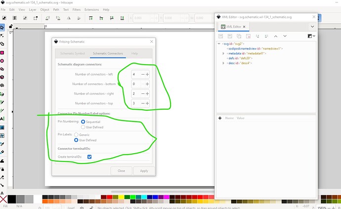
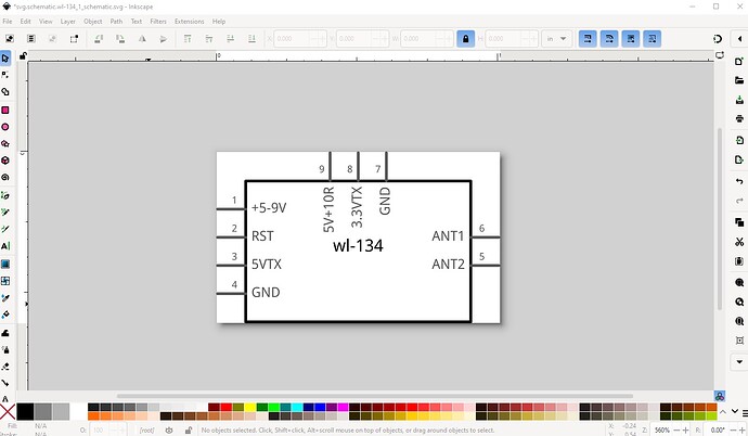
Breadboard is now complete so save it as plain svg and proceed to schematic. For schematic I used Randy’s Inkscape extension for creating Fritzing schematics. First set the sizes and part label
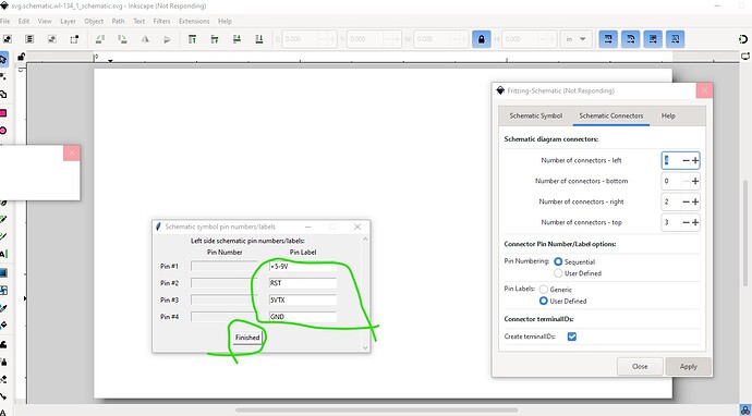
Then set the number of pins on each side
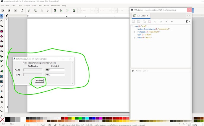
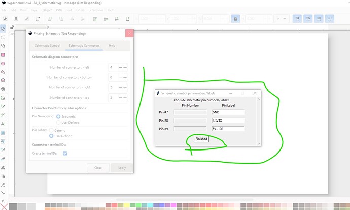
then add the pin names (one side at a time)
which results in a schematic svg like this
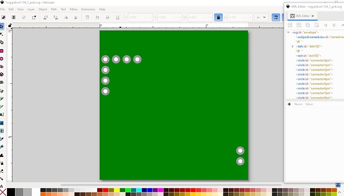
Now on to pcb. Copy the breadboard svg to the pcb svg and edit the pcb svg. Ungroup it and remove all the components except for the connectors and the outline rectangle like this
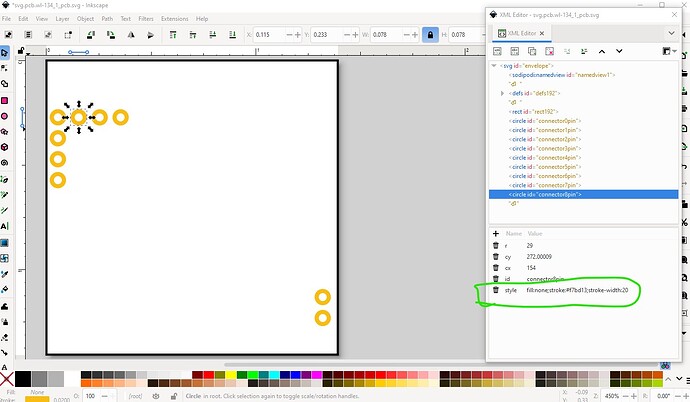
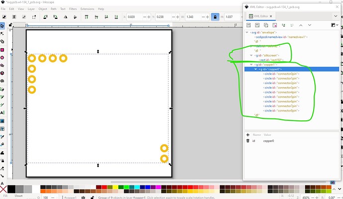
Then turn the outline rectangle in to a 10 thou wide outline for the silkscreen and the connectors in to appropriate form for pcb. Then group the rectangle in to silkscreen and the connectors in to the copper1 and copper0 groups and pcb is done.
Now generate a .fzp file for the part and set the pin descriptions then run the result through FritzingCheckPart.py to clean it up and check it and then produce this .fzpz file by zipping the fzp and 3 svg files. That results in this part which should do what you want.
wl-134.fzpz (14.6 KB)
Peter
