You can use gerbv for gerber previews, much more lightweight.
Right, it was not about the viewbox. The holes were just defined outside any layer.
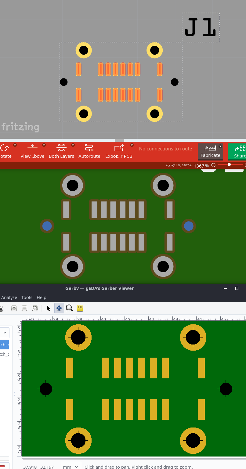
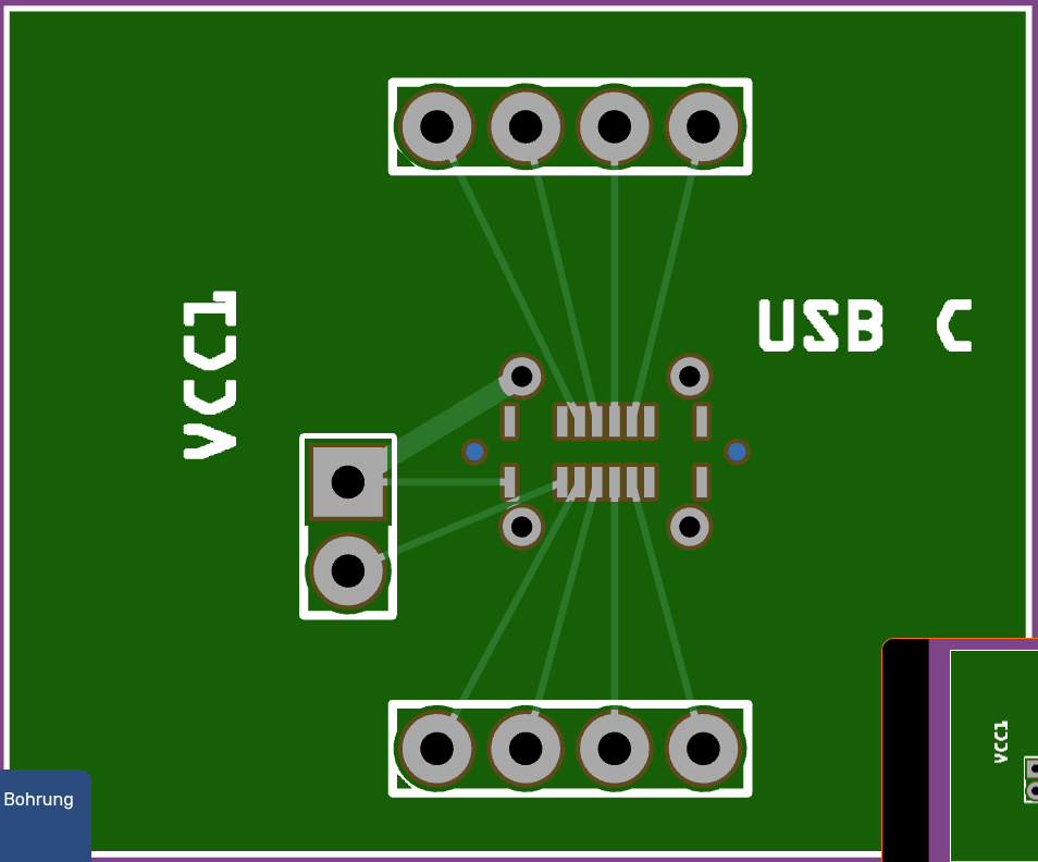
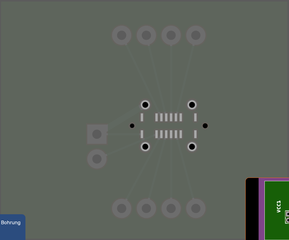
I moved the holes to the copper layer (id=“nonconn0”) and also added black silkscreen for the visual in Fritzing. From top to bottom: Fritzing, Aisler, GerbV
I have another issue with the id=silkscreen. I might need to open a new topic for that.
When I have the id=silkscreen at the bottom, it covers the pads and pins in the part editor, but I’ll look into that some more, or I’ll create a separate topic.
When using your previous file with very thin copper rings, the Fab showed a warning that these would be removed. Which would be correct, but is also irritating.
So, I made acutally made the copper circles (drills) fill="none" stroke="none" stroke-width="0" id="nonconn0"
This won’t cause any warning about removed copper. The since the circles in the copper are now invisible, the silkscreen is required for display.
The Fab again removes the silkscreen, because its on top of the hole, this time without a warning.
Ah yes, I hadn’t even noticed that the warning was gone.
One last question: if the four mounting holes (connector16pad-connector19pad) for the USB socket are supposed to be on both sides, do I need to insert the same graphic element into the copper1 layer?
They should essentially be implemented as THT so that the socket can also be soldered from the bottom.
When you add it there, it should work. You might have to remove the other pads from pcb svg copper0 though. Right now, the definiton is ambiguous: Then connector pads in fzp use copper1 only, in the svg the are in copper0 and copper1.
If you add copper0 in the pcbview definition, the ambiguity might be resolved differently.
Our the fzp_checker.py script in Fritzing part should warn about this already.
Hi Harald,
that looks really good. I have a good feeling about the dimensions and the fit. I placed the USB socket on a paper printout and it looks great.
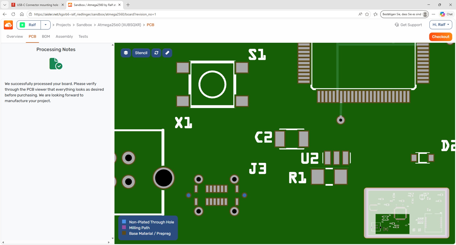
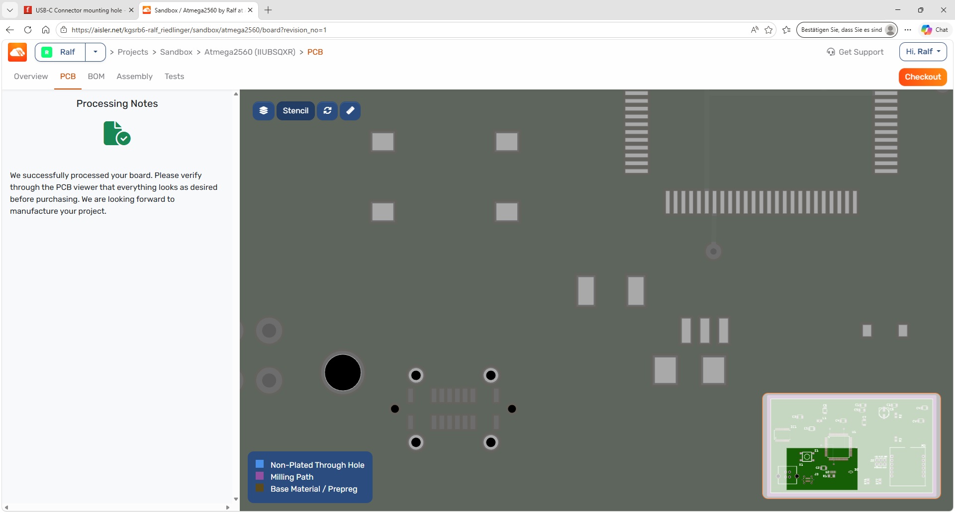
Could you check one more thing though: I’m considering ordering a stencil along with the test PCB. Unfortunately I have no experience with stencils — this would be my first time. In the preview on Aisler, the stencil cut-outs (SMD) are shown in light grey. The pads for THT remain dark grey. But for the new USB-C socket, it’s the other way around. Something might not be quite right with the layers there.
Could you please send me the Fritzing file for this? I can take a look and see if I can find the cause in the fzp file or the corresponding svg file, though I can’t say for sure.
Atmega2560.fzz (75.4 KB)
Sure, here’s the complete Fritzing file. Don’t be surprised — the circuit isn’t finished yet and the components have been thrown onto the board randomly.
I took a look at the files. For the processor, there’s no visible difference in the fzp file.
But in the PCB file there are differences — the pad has the following additional values:
stroke:none
stroke-width:0
stroke-linecap:round
Hi @KjellM,
are the above-mentioned pad properties necessary for SMD stencil cut-outs?
I’m currently expanding my circuit. I’m thinking about connecting the housing of the USB-C connector or the shield plate to GND or PE via a decoupling network (capacitor and resistor).
Hence my question: Can one or all 4 outer solder tabs be made “connectable”?
@KjellM
Can you help us with the stencil questions as well?
I’ve now connected the mounting pads to GND. To avoid an error message, I’ve also added the missing connections to the schematic and the breadboard. Could you check whether that works?
Unfortunately, not all GND connections are in one bus, but I’ll try to change that.
I would change this fzp code:
Hi Harald,
the shield plate now appears to be electrically connected to GND. I can’t see a connection as such, but when I click on it, GND and the shield plate light up at the same time.
I currently favour connecting the shield plate to PE via a capacitor (1206 C0G 2.2nF 1kV). It would therefore be better if the shield plate had its own net — e.g. shield1, shield2, shield3, and shield4.
That way, each user can decide for themselves what to connect the shield plate to.
Even when connecting to GND, there should be some decoupling. On Arduino boards (where there is no PE, so GND has to do the job), this is decoupled via a ferrite bead of type BLM21.
The paste mask (stencil cutout) is currently determined by existence of layers:
pcbView layers contain copper0 → THT for the whole part. No connector gets paste.
pcbView layers contain only copper1 → SMD for the whole part. Every connector gets paste, including a “mounting pin” you’d want drilled.
This is again not sufficient enough for the USB-C connector, like the oblong cutouts, this is a new feature.
I think the currently best workaround to combine SMD and THT is to split it in two part composites:
One with only the pads, that uses copper1. And another one with the mounting holes, that uses both copper0 and copper1.
I tried to find a compromise. I’ve set the PADs so that they appear grey in the stencil view. However, the mounting holes are no longer implemented as THT. So you can only solder the socket from the top. One option would be to place the four holes as a THT component exactly on the socket, so that you can solder the socket from both the top and bottom. Please check that first — only then would I check the socket with the script.