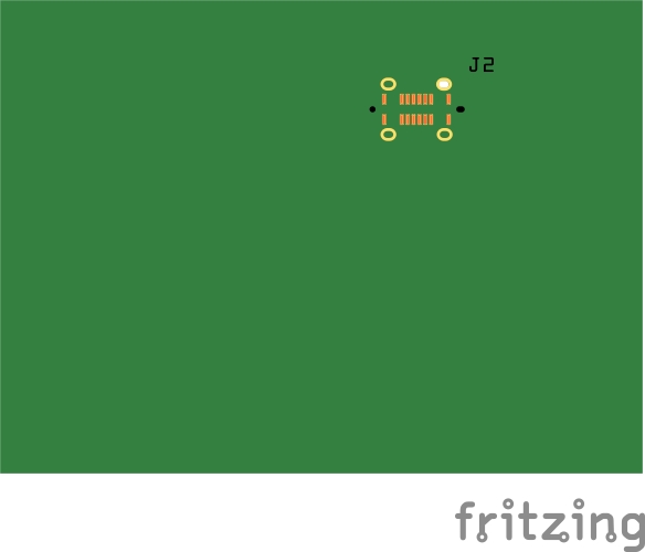
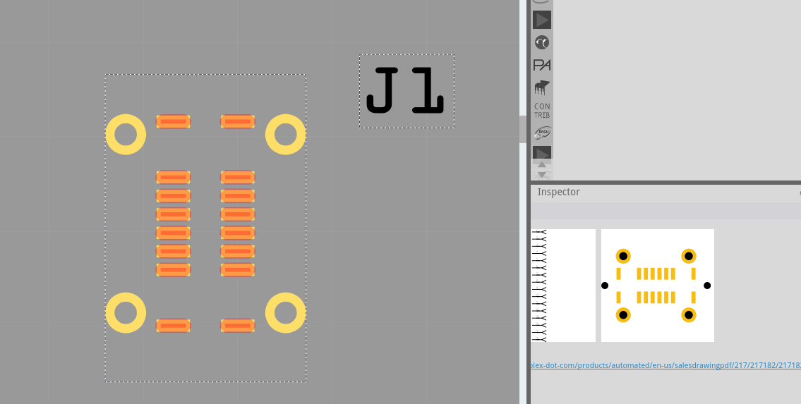
USB-C Connector mounting hole

Good day,

I was unable to find a USB-C connector in the Fritzing parts library, so I wanted to try creating one myself.

Unfortunately, I am not sure which conventions apply to pads in the PCB view. Are the following assumptions correct?

  • SMD pads have the ID connectorXpad, are filled with #f7bd13, and are included in copper0.

  • Pads used for mounting a connector are oval shapes filled with #f7bd13. They are also in the copper0 layer and have the ID connectorXpad. On top of them lies an oval shape filled with “black”. This oval shape has the ID connectorXdrill.

  • Holes that need to be drilled for screw mounting are only a black shape (oval or circular), but still within the copper0 layer.

I am attaching my draft for the footprint.

footprint_usb_1_1

Is the reference for the part file format still up to date?

Gruß Harald Rau!

1 Like

Current state
circular shapes in the copper layer will be drilled. So you could build an oval by “nibbling” – put several overlapping circles next to each other. Depending on the diameter, the FAB would
automatically use this method anyway, because openings below a certain diameter can’t be CNC-routed (the drill bit would be too thin for the sideways load).

Oval drills like in your SVG are currently not directly supported by the gerber export. The closest workaround (and what most FABs would do anyway) is to nibble the oval with overlapping circular drill hits.

Regarding your SVG conventions, your assumptions are mostly correct:

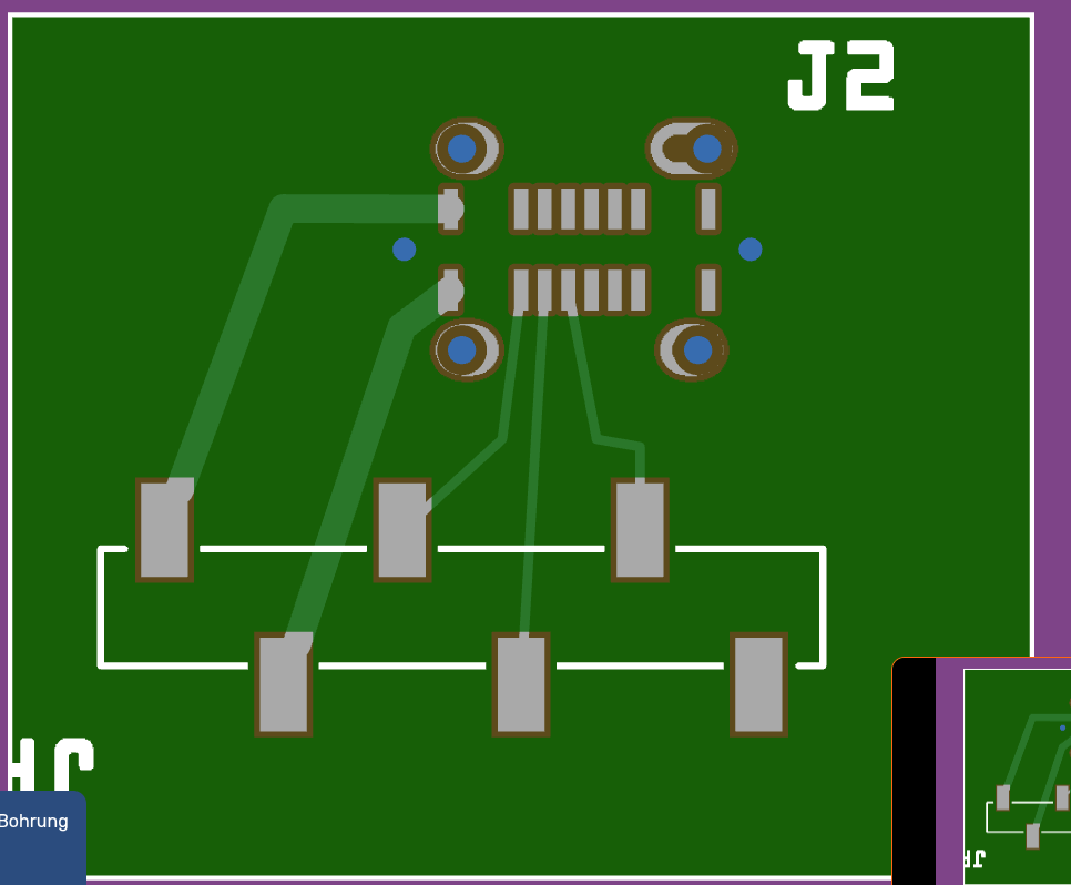
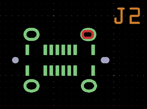
  • SMD pads: id=“connectorXpad”, fill #f7bd13, in copper0 – correct.
  • Through-hole pads: copper shape with id=“connectorXpad” plus a black shape on top with id=“connectorXdrill” – this is the right idea, but note that currently only circles are recognized as drill holes by the
    gerber exporter. Your elements with id=“connectorXdrill” won’t produce drill hits in the current version.
  • Mounting holes: a black circle in copper0 will produce a drill, yes.

Also: your silkscreen layer is spelled skillsreen – should be silkscreen.

Edit: For completness, board outlines support negative shapes. The board should be defined clockwise. Anything counter-clockwise is then a hole and will be drilled our cut out.

Future plans
The idea is to add explicit drill and cut attributes to the SVG part format (for example
fritzing:drill and fritzing:cut attributes , similar to the ‘drill’ attribute currently described at the end of the spec. This would allow something like:

  <svg xmlns="http://www.w3.org/2000/svg"                                                                                                                                                                            
       xmlns:fritzing="http://fritzing.org/xmlns/0.1" ...>                                                                                                                                                           
    <g id="copper1"><g id="copper0">
      <!-- Plated oval slot -- routed to final shape -->                                                                                                                                                             
      <rect fritzing:drill="plated"                                                                                                                                                                                  
            x="46.772" y="179.13" width="33.465" height="23.622"                                                                                                                                                     
            rx="12" ry="12" />                                                                                                                                                                                       
                  
      <!-- Non-plated mounting hole -->                                                                                                                                                                              
      <circle fritzing:drill="non-plated" cx="10" cy="106" r="10" />
                                                                                                                                                                                                                     
      <!-- Board cutout -- tool follows the outline -->                                                                                                                                                              
      <rect fritzing:cut="true"                                                                                                                                                                                      
            x="20" y="20" width="50" height="30" rx="5" ry="5"                                                                                                                                                       
            stroke-width="1.88" fill="none" stroke="black" />                                                                                                                                                        
    </g></g>
  </svg>                                                                                                                                                                                                             

The key distinction: fritzing:drill removes material inside the shape (for holes and slots), while fritzing:cut removes material along the shape outline (for board cutouts, using stroke-width as the kerf). Both
support circles, rects, paths, and arbitrary shapes. The attribute can be set on a element and is inherited by all children.

Non-circular drill shapes would be exported as Excellon rout commands (M15/M16 rout mode)

This is still in the spec/planning stage – not yet implemented.

There is also the issue that ids need to be unique, which is makes using ids for fritzing layers (copper0, copper1, … ) a bit convoluted. So, I don’t think we’ll use id=“drill” like I think I suggested earlier.

Thank you,

that helps me a lot.

I also found a part from Peter where he used the nibbeling. He also used the mounting holes with the id=nonconnX. That also created holes in the Gerber view. If I saw it correctly, the holes (nibbeling) do not touch each other in the example. That would then require later manual reworking.

Does the overlapping of the holes cause no problems during milling? The overlap should certainly be smaller than the radius of the hole, right?

I will incorporate the hints and create the USB-C connector.

Thank you once again!

Best regards, Harald!

Aisler mentions USB-C connnectors as an example for nibbling:

However, in that case, the factory decides about the drill distance, and the gerber file (Fritzing) should just specify the slot.

It looks quite smooth in the picture, so maybe their process works with a overlap bigger than the radius.

Hello Kjell,

I tried a few things. The PCB viewer from Aisler kept throwing an error and ignored the slots. I then contacted their support and received this response:

Hello Harald,

I'm probably a little late, but I still want to get back to you.

In principle, we can manufacture nibbled slots, but they need to be drawn as slots in the design data.
Fritzing does not support this.
Have you ever considered switching to something like LibrePCB?
My feeling is that your requirements go a little beyond what Fritzing is capable of.

Best Regards / Viele Grüße / Meilleures salutations

Patrick Franken from the AISLER Support Team

I had created the connector with overlapping drill holes and non-overlapping drill holes. Aisler removed the extra holes.

PCB View Aisler:

Message in the PCB View:

We have removed one or more drill holes because they partially overlap and
therefore do not meet our minimum spacing requirements. You can highlight the removed
holes by selecting the entries in the list below. Please review the rendering carefully
and adjust your layout if necessary. Please also refer to our design rules and the
relevant article for your board design for more information. If you get stuck, please
contact our

PCB View Fritzing:

…or did I place the holes incorrectly?

Best, Harald!

Hi Harald, could a solution be to merge the adjacent holes into one object beforehand in your CAD program (lnkscape?)? I think it was called “outline”

I’ll take a look at that, hopefully Fritzing will accept it then.

The current Fritzing parts can not be created with proper slots, but it should be possible with a custom PCB. That can use more flexible cut outs.

Good morning,

can you help Ralf? If so, what files do you need for that?

Best,
Harald!

A custom pcb can be created instead of the basic rectangular pcb provided by default. The existing information can be found in the “Learning” section of the main side.
At the top of the forum page, “Main Site” then “Learning” scroll to “PCB View” then “Custom PCB shapes”

Direct link https://fritzing.org/pcb-custom-shape

That supports internal cut outs with any shape you can create with svg (eg Inkscape). Limited by what the fab can do. So as long as you know where the part is to be placed, you can create the associated slot directly in the pcb, instead of in the part.

To use the created svg file, in PCB view select the pdb, and in inspector properties block, click “load image file”.

For other predefined shapes, click the drop down in the “shape” properties.

1 Like

Hi Merlin,

Does that only concern the outer shape of the PCB?

Or should I add the slots to the bare PCB already and then just position the slot pads exactly on top of them?

I’ll put together an example today and upload it here.

Maybe you can take a look and give me your thoughts?

Best, Harald!

Hello Merlin, thank you for your feedback and your idea. A few years ago, I created a PCB in Fritzing that had a custom outline. I drew the outline in Inkscape at the time and – quite intuitively – also included the mounting holes directly in that drawing. I then had the board manufactured by Aisler, but the result was bad: the round holes came out irregular and no longer truly round. See the attached photos.

Afterwards, I contacted Aisler, and they explained everything to me in detail. I don’t remember all the specifics anymore, but the essential point was that holes must not be placed in the outline drawing. Instead, they need to be defined directly on the PCB in Fritzing.


Hi Merlin,

I’ve gone ahead and implemented it, but the socket needs to fit precisely. Ailser can only mill slots with a width of 1.8 mm. However, we have 0.6 mm x 0.85 mm.

I’ve added the slot to the top right of the board as a test. Is that what you had in mind?

Beispiel_Langloch.fzz (25.4 KB)

Best regards, Harald!

As I said, “Limited by what the fab can do”. The concept looks correct in your sketch. I did an export to gerber to have a look at the output, but currently my viewer program is not working, so I could not verify.

Hi,
first of all, thank you very much for the help.
However, I think we need to find a different solution.

In my Gerber view, you can see that the placement is not quite right.

We would need to add guide lines, both on the board and in the PCB view.

Regards, Harald!

I think we’re on the wrong track. I uploaded it to Aisler for testing, and unfortunately it can’t be manufactured. Maybe we should go with round holes after all.
I took some measurements on the socket. The outer 4 solder pads have actual dimensions of 0.52mm x 0.32mm. The specs in the datasheet (0.85mm x 0.6mm) are quite generously sized compared to that. I’d say it’s possible to make it work with a round drill hole too — maybe 0.6mm?
For the two inner through-holes, I also don’t see any need for a slot, especially since both pins on the component are round. We could follow the datasheet here and make both holes d=0.52mm.
I’m not under any time pressure with this project. I’m happy to order a test PCB from Aisler — possibly with different dimensions and test points on the board to measure the solder joints. Soldering is definitely going to be a challenge in itself.

Good, I’m completely with you on that. I’ll finish the socket with round holes as soon as possible. Then you could order a test board. I’ll try to get it done before Thursday.

Best, Harald!

Hi Ralf,
I didn’t manage to get it done before Thursday after all. But I do have a version that I still need to check. The two small holes are 0.52 mm and the four large ones are 6 mm each.

I want to check it in KiCad first. I also got a warning because I’ve already switched one computer to Fritzing 1.7.0. I can’t say how your computer will react.

USB_type_C_rund.fzpz (24.8 KB)

I may still need to make some changes to the drill holes.

Best, Harald!

The two outer holes are missing. I think this is because they are outside the viewbox.

There is no issue loading the part in 1.0.6, but mixing both versions on the same computer might cause issues: The way parts are stored has changed, and the old versions won’t understand parts imported by the new version.

I think I made the mistake of drawing the two holes outside the silkscreen.

Also, I assigned id=nonconnect to the two black holes. Is that correct? I could of course also draw them as a PIN, but then they would have copper around the hole.

In Fritzing 1.0.6 it looks like this:

At Aisler it looks like this:

If I manage to download KiCad on the ICE train, I’ll check the Gerber view with the drill holes once more.

USB_type_C_rund.fzpz (26.1 KB)

Best regards, Harald!