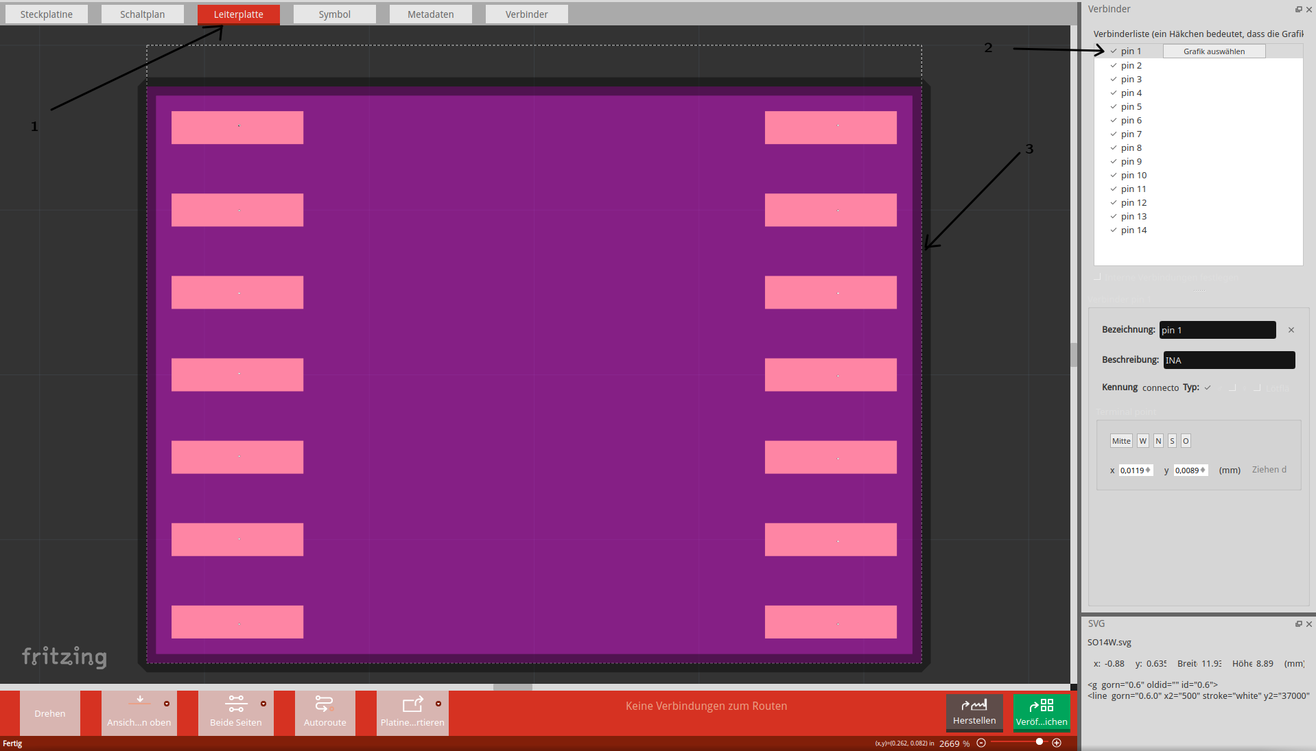
I tried to create me own part for fritzing, but I struggle with wirings connection surfaces.
I have problems to create the pads for the soldering.
How can I introduce the soldering surfaces in the wiring sheme?
Aim is to connect the wires on the pin and not in the middle of the part.
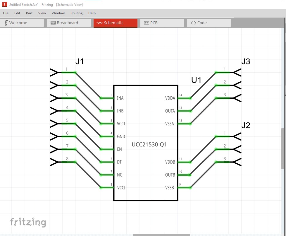
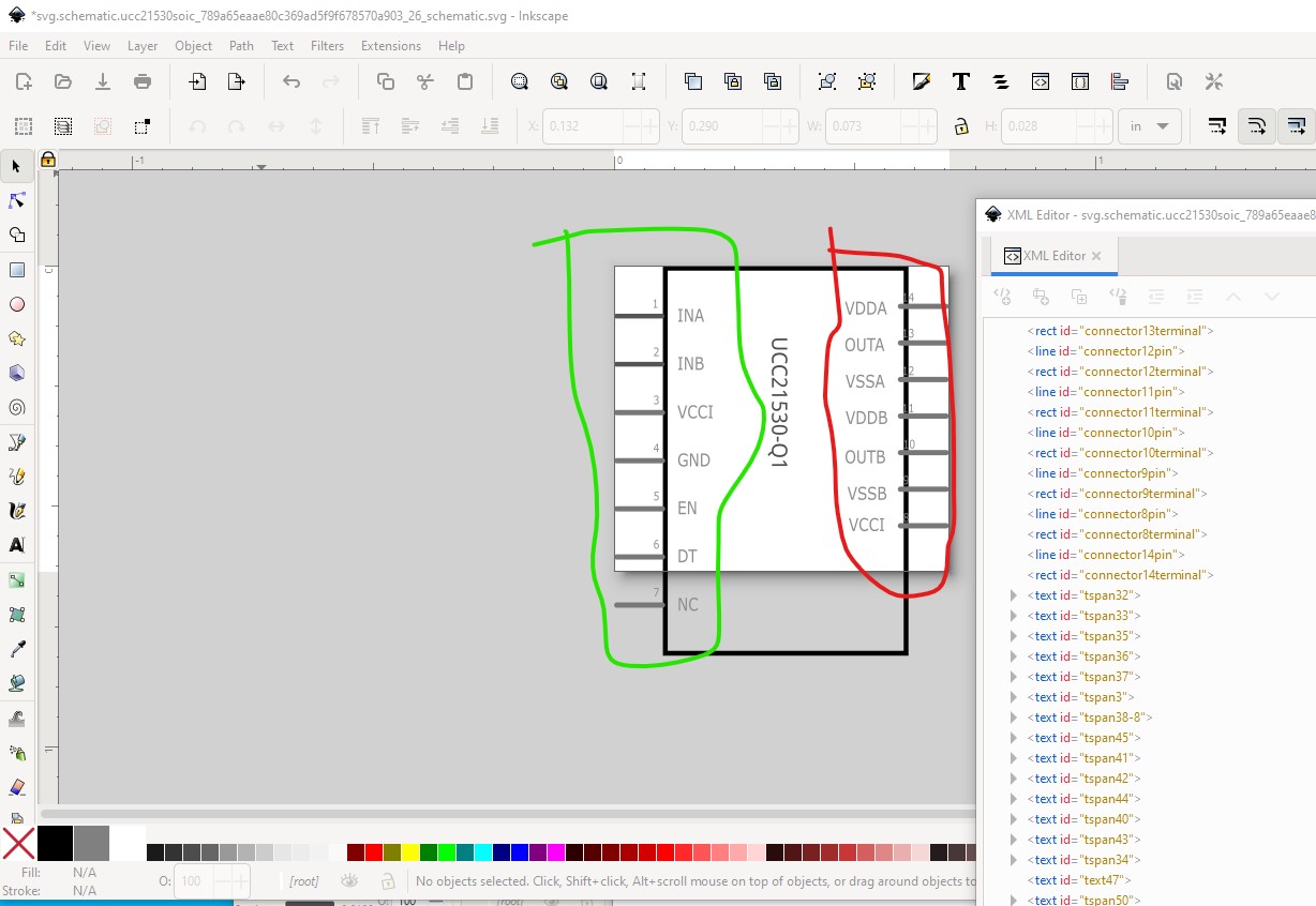
I see in the editor the following view.
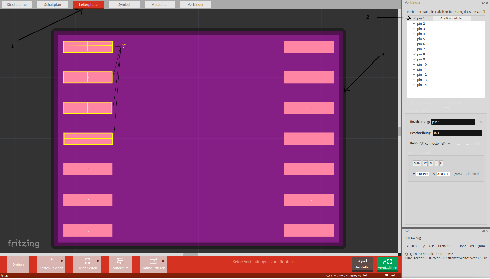
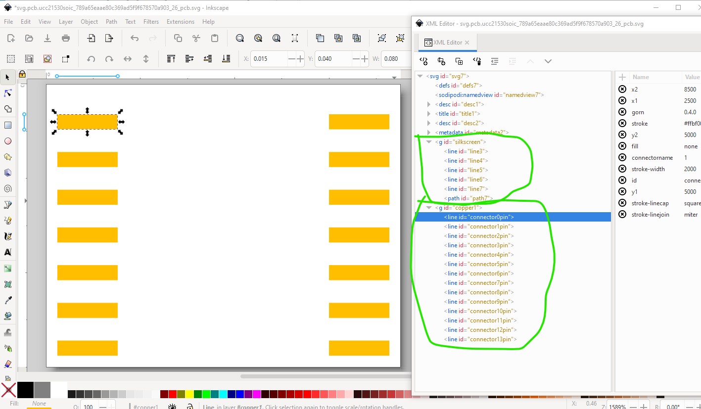
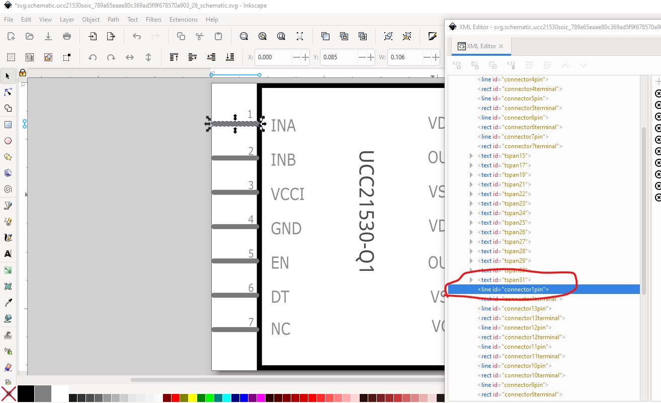
For PIN 1- 14 I can only select the mangenta surface, but I guess I need additional frames on the pad location. On the second picture I painted the expected frames yellow…
How can I create this pads?
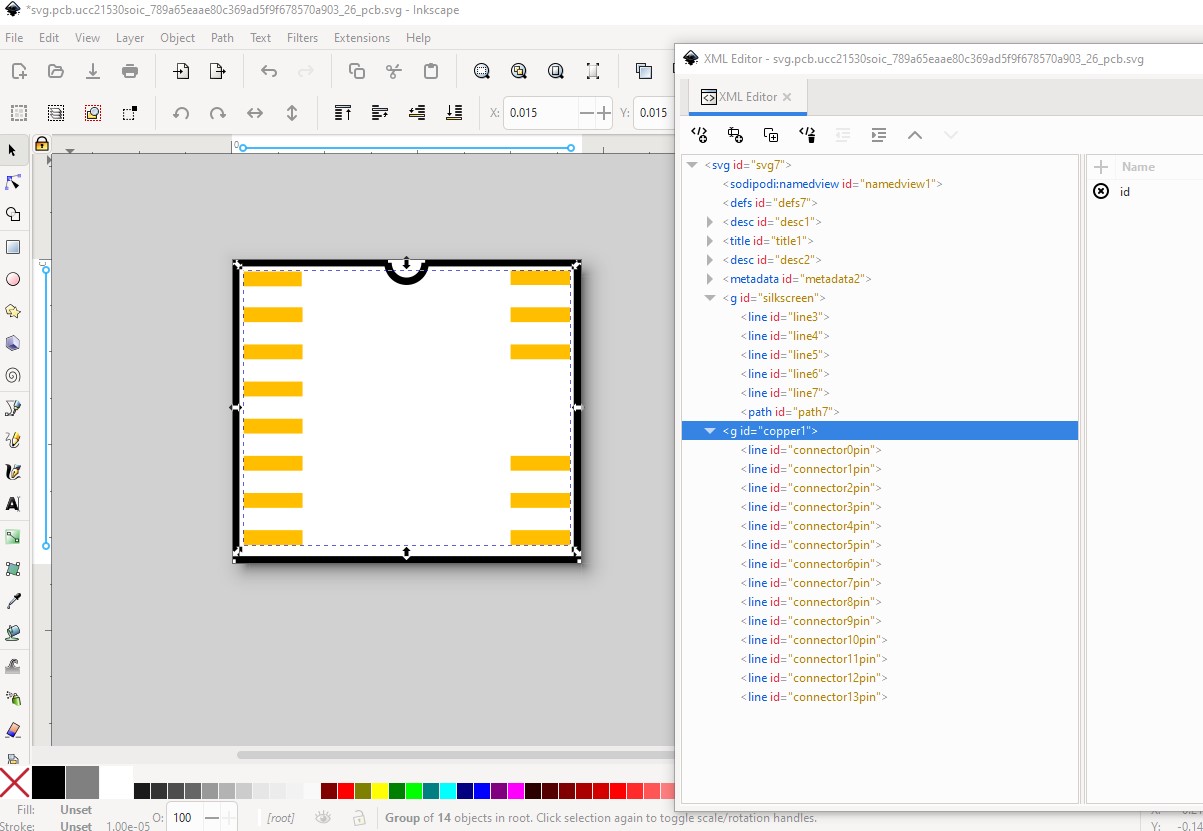
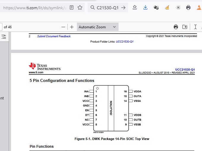
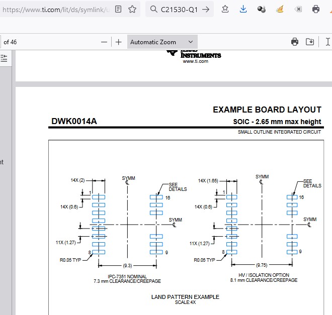
Your part has a variety of problems . The most serious one is that the pcb footprint in the data sheet is not SOIC14 as stated but a modified version. From the data sheet the footprint should be
I haven’t yet finished checking the pad spacing of the current footprint (but it appears somewhat incorrect according to the datasheet.) The other problems in the part are likely mistakes introduced by the Parts editor and a misunderstanding of how parts must be configured. The red rectangle in pcb is because some of the pins defined in the .fzp file are not in the pcb svg which causes the red rectangle and a connection to the center of the part. Reading this tutorial may help explain what needs to happen to make a successful part (I typically edit the files directly and don’t use parts editor.)
I had mostly fixed up the part before I checked the data sheet and saw the footprint was incorrect, I’ll fix that up and post a fixed part and more explanation of what is wrong with the initial part.
edit:
OK here is the completed part and what I did to it (and found wrong) in the original.
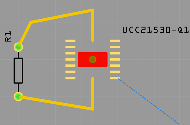
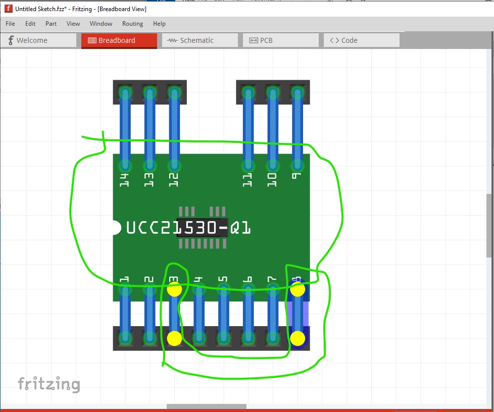
Pins 3 and 8 (VCCI) are internally connected according to the data sheet so they are bused here to indicate that. Clicking on one pin will also light up the other and anything connected to it yellow to indicate they are connected. As noted the chip is mounted on an adapter board that will work on a breadboard again as is standard as an SMD IC needs the adapter board to fit on the breadboard.
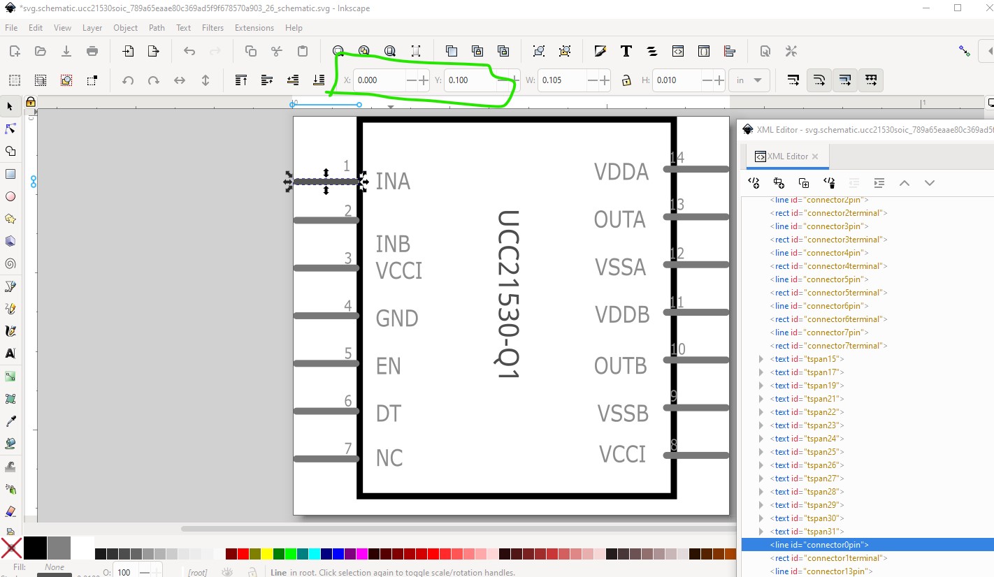
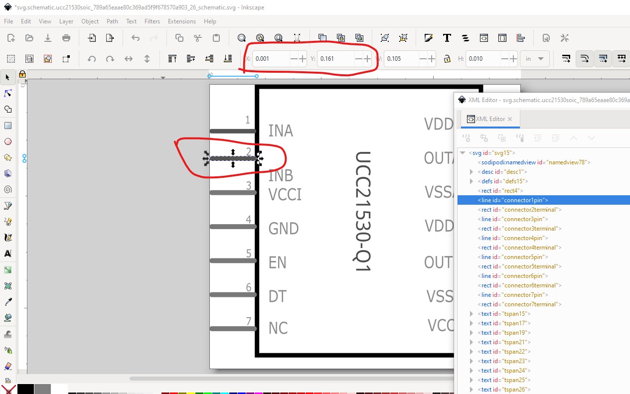
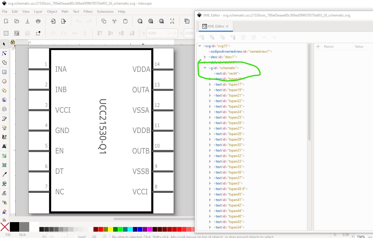
Adjusted to match the data sheet layout and colors and spacing so the pins align to the 0.1in grid as they are supposed to (this is the original schematic)
in the original (as we see here) they are not on 0.1in boundaries. Here the left has been corrected and the right is the original and the rectangle has been increased to the correct size.
once that is done the entire svg needs to be grouped and that group named “schematic” or whatever this line in the .fzp file says which will normally be schematic as it is here (circled in green in the image!)
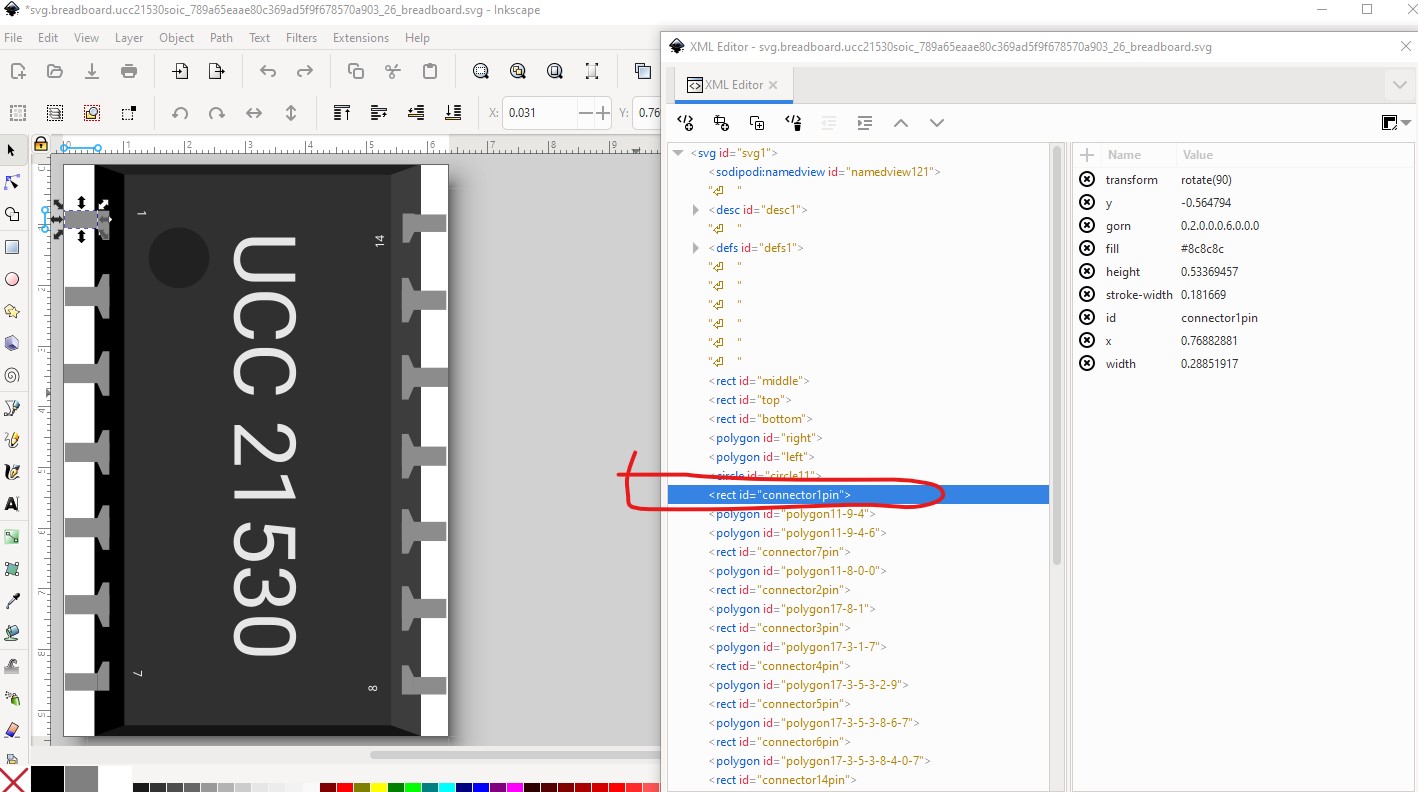
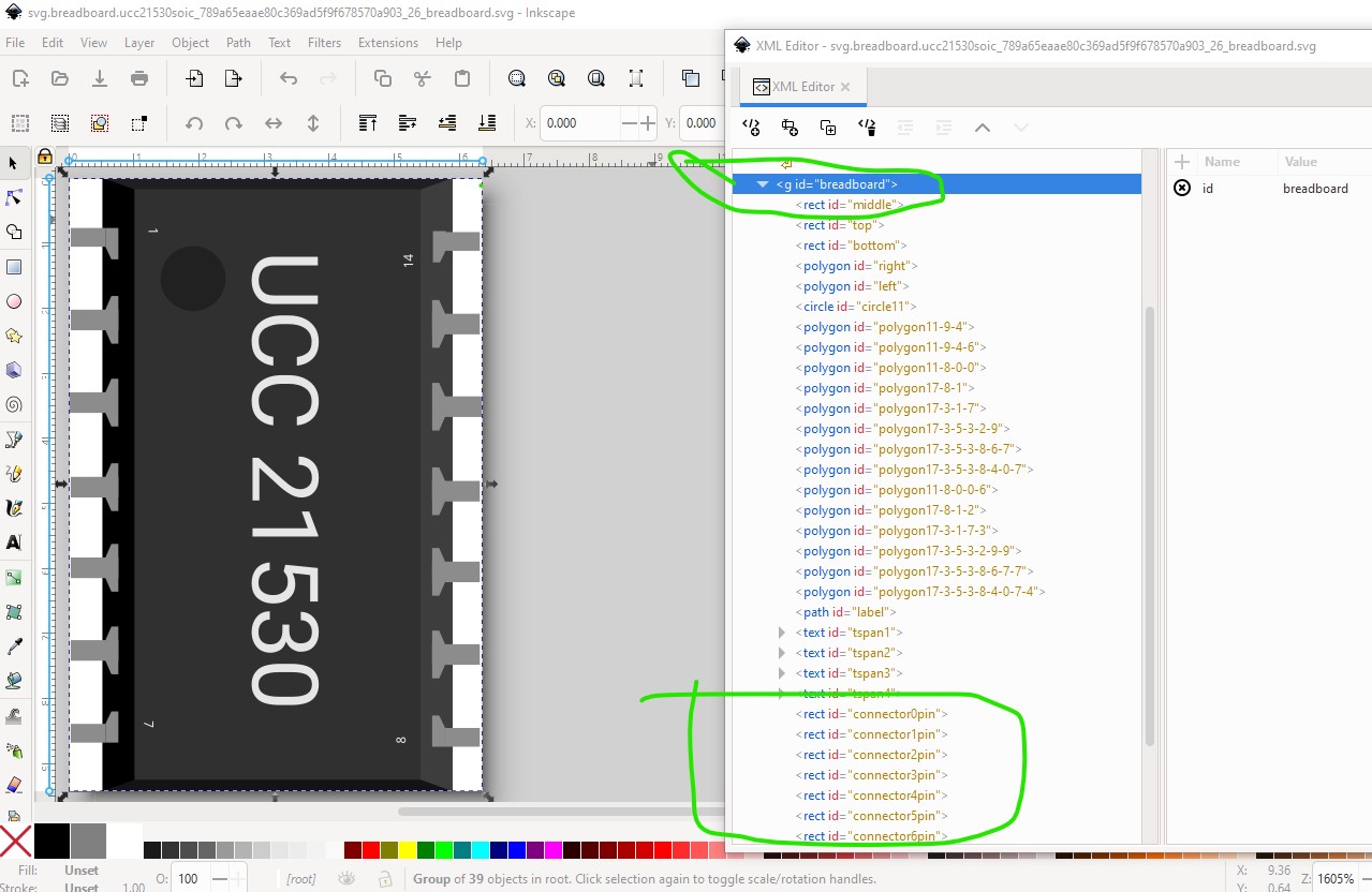
the layerid parameter needs to match the group name in the schematic svg. If it is missing the part will not export as an image (that is the only effect I am aware of, but it is annoying when missing!) The same is true of breadboard and pcb. This is the original breadboard as noted it needs an adapter board and the pins need to start at pin0 (not pin1 as here!)
Hope this helps, if you have questions feel free to ask!
edit2:
Forgot one issue: FritzingCheckPart.py flagged an error in schematic where the font family is
“font-family=”‘Droid Droid Sans’"
that is invalid and Fritzing will substitute it with either ‘Droid Sans’ or OCRA. So I edited the svg and replaced all occurrences of “font-family=”‘Droid Droid Sans’" with “font-family=”‘Droid Sans’" which clears the warning.