Hi Fritzing group! I’ve been using the software for a while now and it’s great and very easy, buut now I want to add a couple of super basic parts, or even just one part!
I basically want a ‘via’ which has an oblong outline - ie an oblong pad.
I’ve spent ages looking around about parts creation and it really is totally over my head - I can succesfully import silkscreen graphics I draw in Inkscape, and even draw custom copper trace layers and import them fine, but I simply can’t figure out a way of doing this thing, which in my mind should be very very easy. I should add I don’t code, I just draw things, I can follow instructions but do get lost in the examples I’ve followed as they all seem to be for rather complicated parts and I really don’t ‘computer’ much! (though I guess one should follow all the steps even for a simple part like a via!) In fact I did think the easiest thing might be to simply be able to draw a custom soldermask shape with a copper layer underneath with cutouts in the mask that are oblong and a drill hole in the middle!
I did try to EDIT a via using the instructions, but I don’t appear to be able to edit vias?
It is a simple task to do that for a specified pad diameter and hole size. The harder task, which would require a code change, is to make that variable (i.e. change the hole size or pad diameter.) as Fritzing creates vias and some other things (such as headers) on the fly rather than as parts. This part creates an oblong pad (copied from a header I made that will route traces between the pins) with the hole sized for a 0.1in header (0.038in hole size.) To change the hole size you need to edit the pcb svg with Inkscape (or other svg editor, but hole size will likely be set differently) and use this calculation to set the hole size (only for Inkscape!)
Hi Peter, ah thank you for that! I have managed to load that as a part now, but I’ll have to dig in to how to export it into Inkscape and edit it, and then re-importing - which is something I never understood I must say! I think with traces and images it is rather easy once one has the hang of what Fritzing likes in the way of SVG files, but I really don’t understand (yet) how to get from SVG → part (FZPZ file).
But that is exactly one of the pads I was after, the other main one was a pad for soldering wires to which I thought would be nice at 0.075" wide by 0.1125" high with a 1mm hole. I’ll see if I can work through some more youtube videos today and make some notes, thank you for the pointer and starter!
A fzpz file is a zipped set of a .fzp file and 4 (1 in the case of the pad) svg file. To edit it, just unzip the fzpz and edit the svg then rezip both the fzp and svg to a fzpz file again. This set of tutorials may help as well
I changed the SVG, and checked XML in Inkscape to see it still said copper1 and copper0, and generaly tried a few things (plain SVG, etc) but when I zip it with the other file (I’m on a mac so use ‘compress file’ and change extension to .fzpz) and try and load it into Fritzing it doesn’t work, have I done something silly?
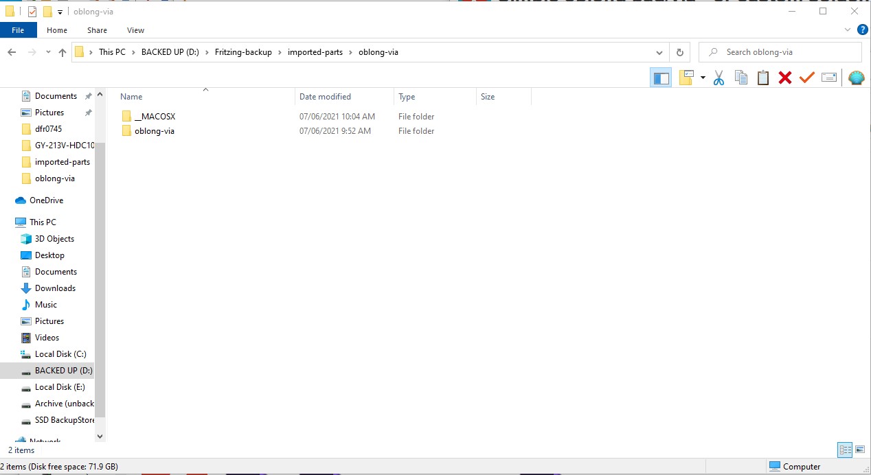
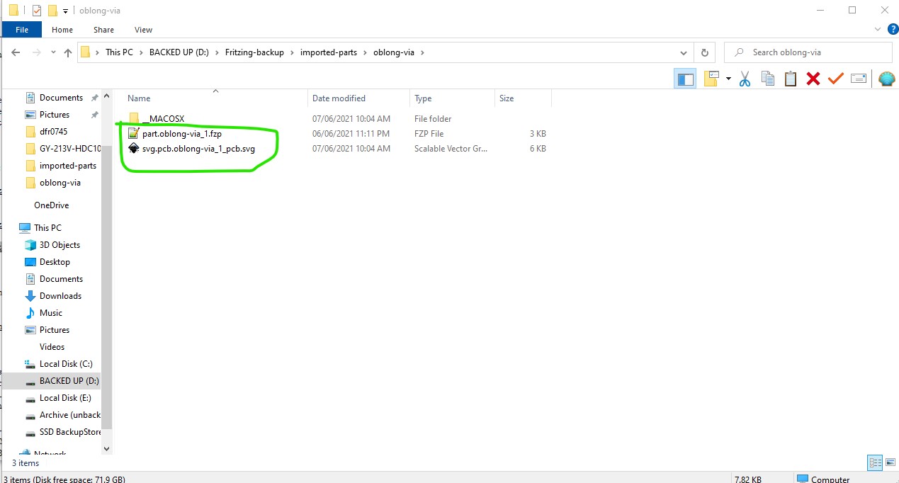
I moved the files in the oblong-via directory up one level so they are where Fritzing is expecting to find them (it will ignore the _MACOS file which I assume MacOS needs.) The loader won’t look in a directory, it expects the .fzp and svg files to be in the top directory of the .fzpz file. I usually use 7zip (which I think will run on a Mac) to zip the files up if you can’t find a way to get the files in to the top directory.
Ah, thank you - I did mention I was not very ‘computer’ haha, so following your advice I have successfully zipped and given the correct extension, so I no longer get an error message when trying to load the part into fritzing… BUT even though I have renamed both files of the part (the SVG and FZP) oblong-via_2, it’s telling me that oblong-via_1 is already loaded? I can’t see any reference in the Inkscape SVG XML to this name - or anywhere now I have renamed them, is it ‘hidden’ somewhere in the .fzp file?..
On another topic, whilst I was here I have now discovered how to import custom PCB shape with cutouts and NOT have a totally glitchy gerber plot, so it’s not all bad news!
The trip point is in the .fzp file. You need to change the moduleId in the first line to something different if you have the original part loaded (or want to load it later.) As well the fzp and svg file names need to be unique as well (or they will overwrite the current ones and break the original part.) So your part needs to change the moduleId here in the part.oblong-via_1.fzp file from
and the file name needs to change to part.oblong-via-bigger_1.fzp (or any file name that you choose) and then the svg file needs a name change to something like svg.pcb.oblong-via-bigger_1_pcb.svg with a corresponding change to this part of the fzp file as well
all the instances of “oblong-via_1_pcb.svg” need to change to the new file name such as “oblong-via-bigger_1_pcb.svg” so they are unique. It is probably easiest to do this using a text editor on the part.oblong-via_1.fzp file.
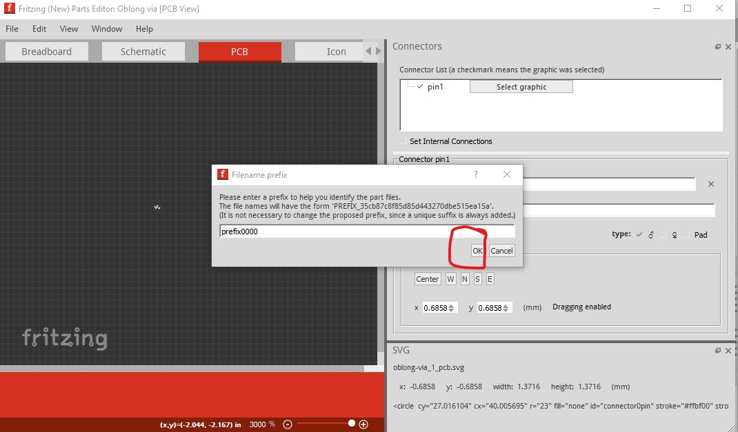
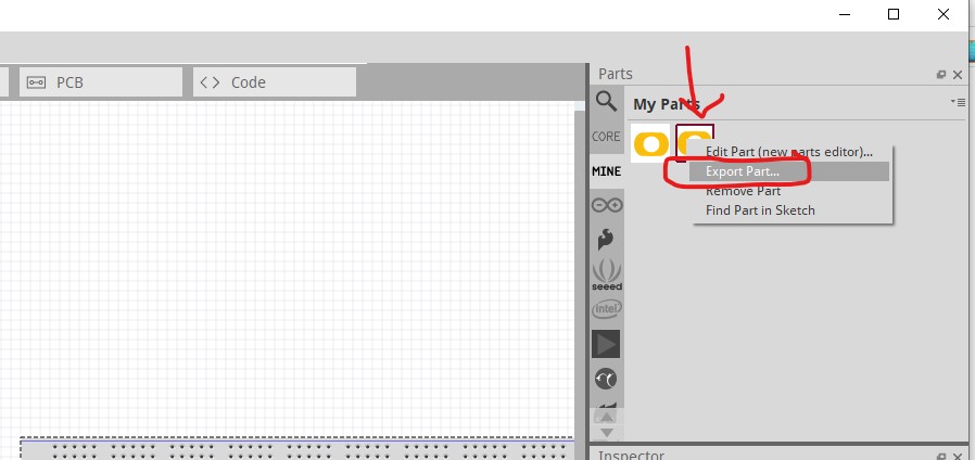
edit: I was going to say that the parts editor (via making a new part) is the easiest way to change the moduleId and file names, but this particular part trips a bug in Fritzing which crashes the parts editor so don’t try and edit it with the parts editor. I’ll have a look at figuring out what it is unhappy about (likely missing views) and report the bug(s).
I just replaced the original part oblong-via.fzpz at the top of this post with a part that can be edited by the parts editor (it wants layerIds even if they aren’t used.) So the easy way to modify this is to
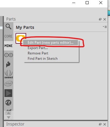
load the fixed part in to Fritzing then edit it with the parts editor
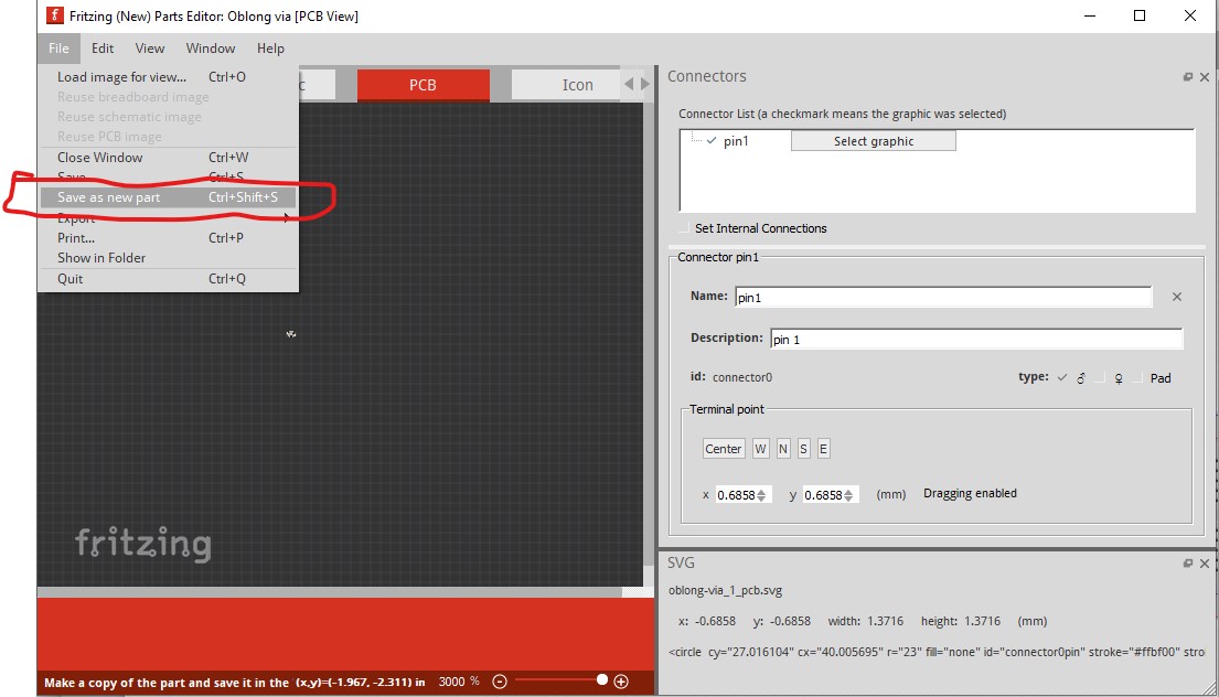
then without making any changes click File->save as new part
Hmm, I think this has rather got beyond me now, I’ve edited the SVG and saved and zipped but now it says ‘error reading file - part not found’ when I try and load it - at first I was getting an error about the prefis, but managed to sort that out. It’s probably something silly!
You are most likely missing the .fzp file in the zip. That is the usual reason for part not found. There should be a part.part-name.fzp file and a svg.pcb.partname.pcb.svg file in the zip.