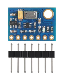
Does anyone happen to know about or possess the MS5611 pressure sensor file in .fpzp format?
Type
I did not read this
Breakout board, sub assembly, plug in module (A)
Antenna (AE)
Battery (BT)
Capacitor (C)
Diode (D)
Display (DS)
Fuse (F)
Hardware , mounting screws, etc. (H)
Jack, fixed part of a connector pair, header (J)
Relay (K)
Inductor, Coil, Ferrite bead (L)
Loudspeaker, Buzzer (LS)
Motor (M)
Microphone (MK)
Plug, moveable part of a connector pair (P)
Transistor (Q)
Resistor (R)
Thermistor (RT)
Varistor (RV)
Switch (S)
Transformer (T)
Integrated Circuit (IC)
Crystal, Oscillator (Y)
Zender diode (Z)
Other (please specifiy)
Good morning,
I can try to adapt this component.
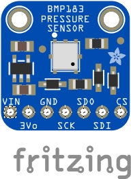
However, I would need the exact dimensions, especially for the hole and the position of the pins.
Is there a datasheet, or can you measure it?
Best regards, Harald!
Module Length: 19 mm.
Module Width: 13 mm.
Pin Spacing (Pitch): 2.54 mm.
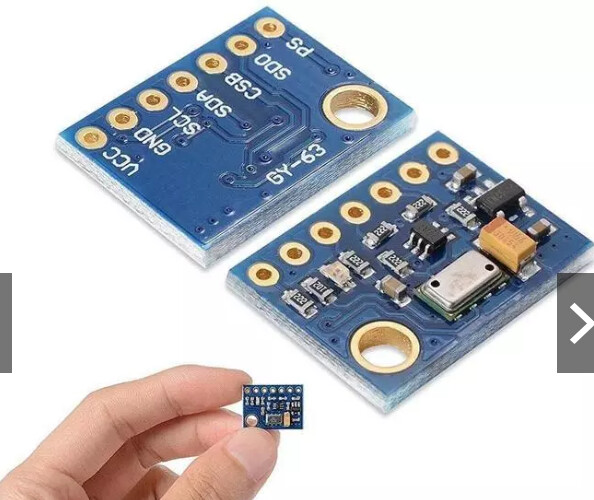
Pin Configuration: The module features 7 pins in the following order: VCC, GND, SCL, SDA, CSB, SDO, and PS.
The linear distance from the center of the first pin to the seventh pin is 15.24 mm (calculated as 6 spaces between pins multiplied by 2.54 mm). The module’s main mounting hole is generally designed for an M3 screw, with a hole diameter of approximately 3 mm.
Great, do you also have the position measurements for the mounting hole from the center to the edge?
Since I wasn’t quite sure how to measure it, I asked online and received this answer:
"Hole Radius (to the inner edge of the hole): The mounting holes on this module are generally designed to accommodate M3 bolts, which have a diameter of approximately 3.0 mm to 3.2 mm. Therefore, the distance from the center of the hole to its edge (the radius) is about 1.5 mm to 1.6 mm.
Hole-to-PCB-Edge Offset (to the outer edge of the board): To maintain structural integrity and prevent the circuit board from cracking easily when bolted down, manufacturers typically position the center of the mounting hole 2.5 mm to 3.0 mm away from the outermost edge of the PCB. This arrangement leaves approximately 1 mm to 1.5 mm of solid material (FR4) between the edge of the bolt hole and the outer edge of the board."
Has this answer been helpful?
Yeah, I’ll try to make something work with it — the hole isn’t critical anyway. I’ll get back to you shortly with an initial suggestion…
Thank you very much; I had searched various websites but couldn’t find a suitable sensor.
So, here’s the breadboard view for now. If you’re happy with it, I’ll do the rest. It’s not that hard — I think I’ll get it done tonight.

Looks a bit small, but that’s the specified size.
Cheers, Harald!
Yes, this is perfect; you can proceed with it.
Hi,
I hope this version works. I haven’t checked it with the script just now, but it should work.
MS5611-01BA03.fzpz (10.9 KB)
Regards, Harald!

Wow, this is perfect. I’ve tried it out and it works great; as a beginner, I’m really grateful, because I had looked everywhere for this without success.
Thank you so much, Harald.
Great, good luck!
Best, Harald!
Hey Harald,
do you happen to know how to set up my heat dissipation area for a TO-220 package?
I just downloaded the new version 8 — looks great.
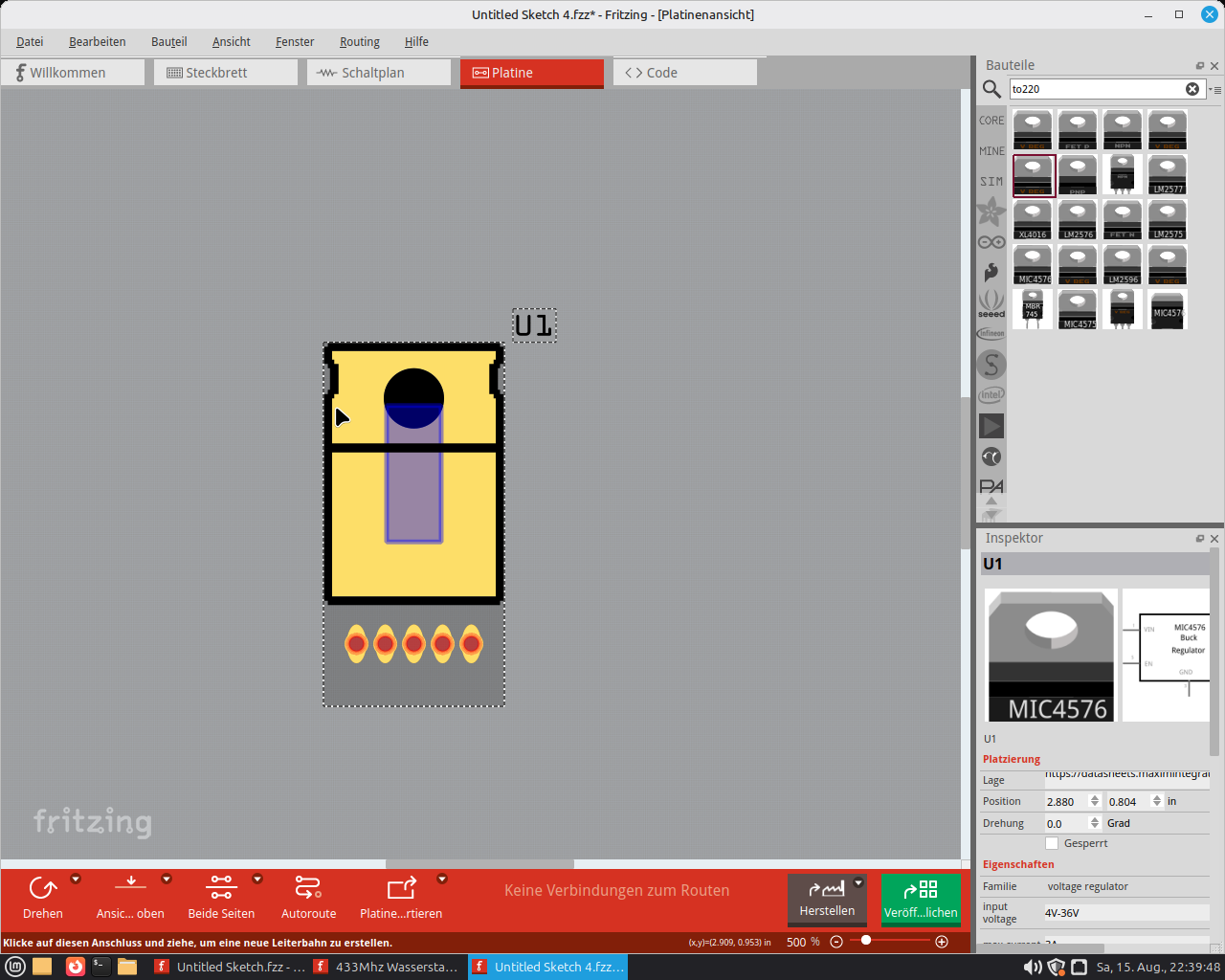
I know how to place the TO-220 standing upright, no problem there, but I don’t want to mount it upright with a heatsink and thermal pad — I want to lay it flat and connect it to a copper area. All I have is a Cu fill covering the whole board, I can exclude part of it and I can place a pad — do I have to use that? It would be great if it worked like an SMD transistor: three strips on the bottom and a pad on top for soldering.
any tips?
Thanks in advance
Hans Werner
Hi Werner,
Take a look at the ESP32-C3 and the ESP32-S1. Are you thinking of something like this area?
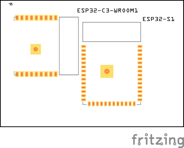
Cheers, Harald!
Hey Harald,
Already sorted it out… I used vias and by adjusting the size
I created my pads…
Sounds good — all the best going forward!!!
Good evening Harald, looks like I celebrated too soon!!!
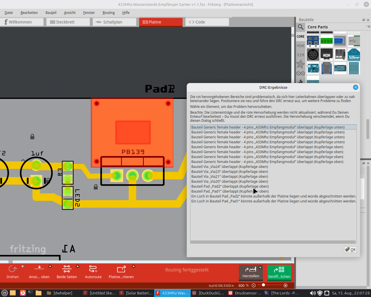
I wanted to mount a TO220 not standing upright but lying flat with a pad for heat dissipation — I used 2x pads, 1x on top and 1x on the bottom = stacked on top of each other, and 4x vias so that I have the pad area on top also on the bottom = better cooling. Unfortunately the new Fritzing is complaining that there would be a problem because something would overlap — part on top, part on the bottom… or is there maybe in the new version 8… perhaps TO220 components that can already be placed pre-bent on the board?
That would save me from what I just tried…