Yes, I can see it. I think I can rework it. I’d then design the schematic the same way as a three-terminal voltage regulator. Could I take the PCB layout from the MIC45676 and reduce it to 3 THT holes?
Great, is a version of an N-mos possible or are they all one and the same?
then they put the 8th on and you always tend to forget those little things otherwise, better that way.
Hello,
yes, that’s certainly possible. Let me attach the example so we’re on the same page.
The symbol should stay as it is.
Beispiel_FET.fzz (1.3 KB)
Best, Harald
…though it might not happen until Tuesday…
Hey Harald…I can’t see the file like that…but there are also accessories…
is this the part? if so great!!
can the cooling surface be extended by about 1-2mm all around or is the surface enough, I can see that the TO220 is lying on the board but how am I supposed to solder it down?
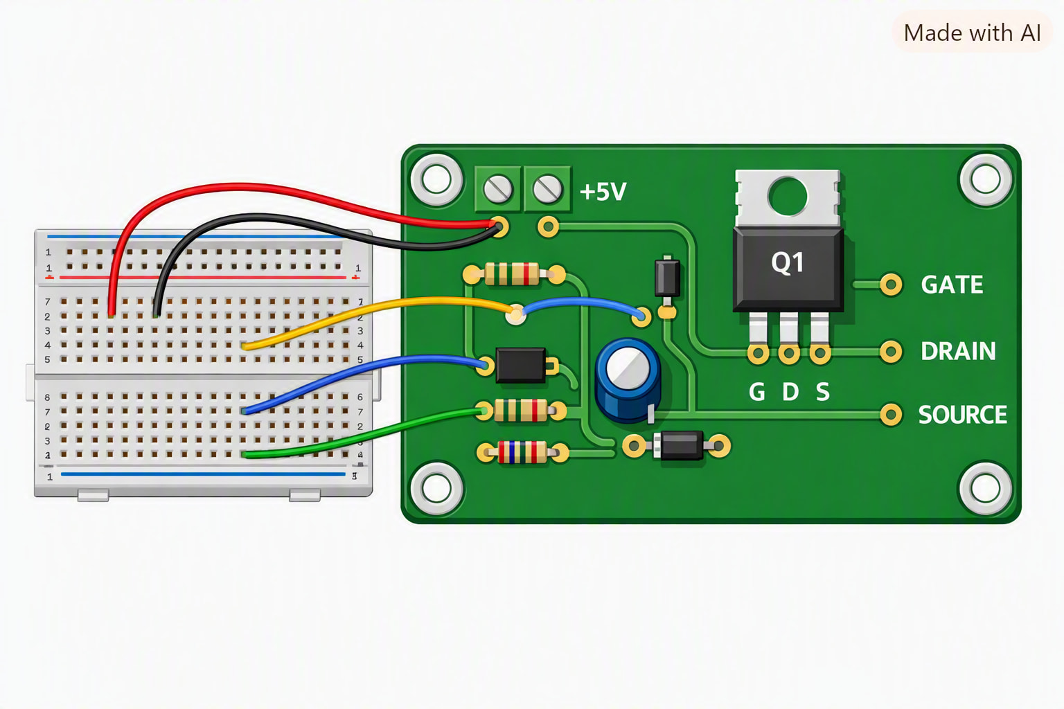
Yes, I’ll try. Tomorrow we’re on the road, but on Tuesday I’ll give it a go.
maybe also an appropriate hole for the purpose of giving a choice between either screwing to a heatsink or soldering… (maybe on both sides too?)
I’m now setting the pad for soldering to 11mm x 15mm. I hope that’s enough.
I’m also adding three THT pads for soldering.
Best regards, Harald!
So, I’ve created a version now. The Gerber view looks promising. The hole is drilled and the solder pad is filled with copper.
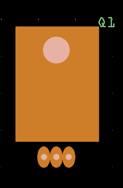
I would run the check script one more time though — especially the older templates often have the wrong color.
Have a look at the part first.
N-Channel_MOSFET_Lötpad.fzpz (8.4 KB)
Best, Harald!
Good evening Harald, in principle yes …
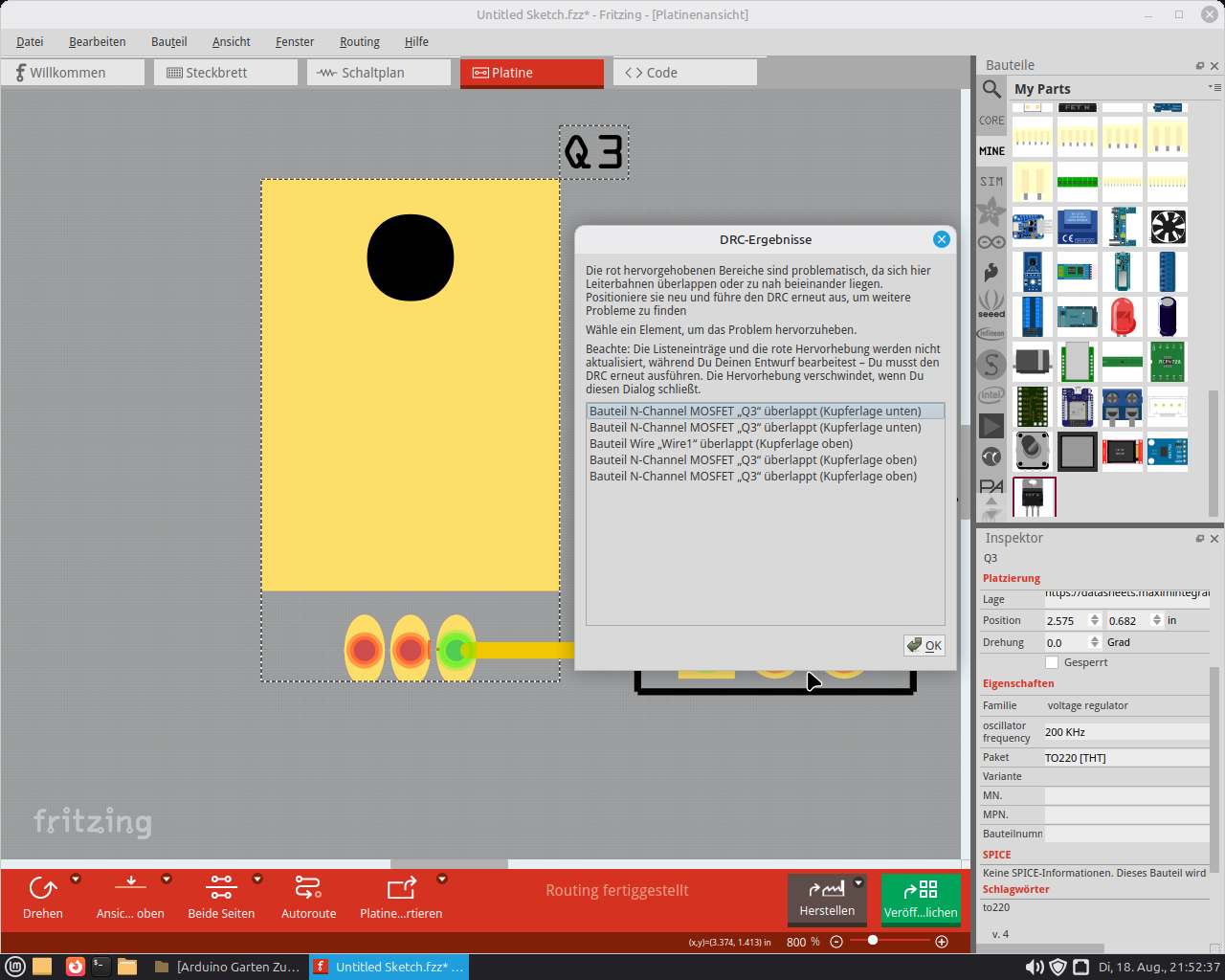
if it weren’t for the solder pads / holes being too wide… I had connected something rough once and the check complained about it…
Good, those weird ellipses were bothering me anyway. I’ll just remove them so that only the normal THT holes remain. Is that alright?
Hey Harald, my motto is… if it doesn’t fit, just make it fit…!!!
As long as the function isn’t affected I don’t care, the main thing is that everything can be connected properly and the test program stops complaining…
Ok, I’ll check the spacing again, I think tonight…
Good thing you checked it. The spacing was WRONG!
I’ve now also run the part through checker.py again. Everything should be correct now.
python3 fzp_checker.py --fix part.N_Channel_MOSFET_Lötfläche_87e34abe5ea66c7fa88ca92d451af322_18.fzp
Checking 1 FZP files
Scanning file: part.N_Channel_MOSFET_Lötfläche_87e34abe5ea66c7fa88ca92d451af322_18.fzp
Checking SVG file: svg.icon.N_Channel_MOSFET_Lötfläche_9269b924143b74efad61439f8b468957_2_icon.svg
Checking SVG file: svg.breadboard.N_Channel_MOSFET_Lötfläche_9269b924143b74efad61439f8b468957_2_breadboard.svg
Checking SVG file: svg.schematic.N_Channel_MOSFET_Lötfläche_9269b924143b74efad61439f8b468957_2_schematic.svg
Checking SVG file: svg.pcb.N_Channel_MOSFET_Lötfläche_9269b924143b74efad61439f8b468957_2_pcb.svg

Summary:
  Files checked: 1
  Checks run: 62
  Errors found: 0
  Errors fixed: 0

File Details:
  part.N_Channel_MOSFET_Lötfläche_87e34abe5ea66c7fa88ca92d451af322_18.fzp: ✓ CLEAN
    └── svg.breadboard.N_Channel_MOSFET_Lötfläche_9269b924143b74efad61439f8b468957_2_breadboard.svg: ✓ CLEAN
    └── svg.icon.N_Channel_MOSFET_Lötfläche_9269b924143b74efad61439f8b468957_2_icon.svg: ✓ CLEAN
    └── svg.pcb.N_Channel_MOSFET_Lötfläche_9269b924143b74efad61439f8b468957_2_pcb.svg: ✓ CLEAN
    └── svg.schematic.N_Channel_MOSFET_Lötfläche_9269b924143b74efad61439f8b468957_2_schematic.svg: ✓ CLEAN
Here’s the part — you’ll need to delete it on your end first. I always have trouble with that, because old leftover files tend to hang around in the Linux profile.
N_Chennel_MOSFET_SolderPad.fzpz (8.8 KB)
Cheers, Harald!
I didn’t save your part in my Parts at all…
And please don’t stress yourself out… there’s no rush, no need to panic!!!
GREAT!!! HAROLD
 Works perfectly!!! MERCY THANK YOU!!!
Sounds good — good luck!
Best, Harald!
Thank you!!! for your work!