For an OLED of the same display size with a built in charge pump and a different connector, the QG-2864KSWEG01, https://datasheet.lcsc.com/szlcsc/1811151642_Shenzhen-Allvision-Tech-QG-2864KSWEG01_C85007.pdf here’s my first go: 30 pin OLEDv1.fzpz (9.9 KB)
I certainly need help with the 30 pin OLEDv1.fzpz
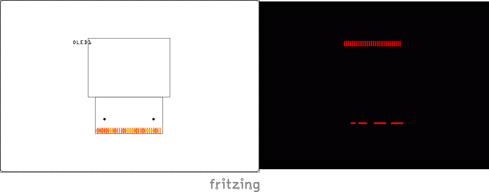
The problem that occurs with it can be demonstrated when the part is placed and traces are connected to its pads. When subsequently exporting the Gerber files, the traces appear in the correct location but the pads end up near the top left of the silkscreen:
Sincere thanks in advance for input!
A screen shot is not really (normally) enough to go on for resolving a problem like this. The actual sketch file (.fzz) would be a lot better. In addition, the single part in the view provides no real context. It needs extra content to see that the gerber view is not a simple offset with the complete content. Here is a sketch file I created, so that I could reproduced the problem, plus screen shots from Fritzing PCB and the gerber output. I also moved one of the pins in (a copy of) the oled part, to use as a ‘key’ in the views, to check if things are being flipped or rotated.
oled-test.fzz (12.4 KB)
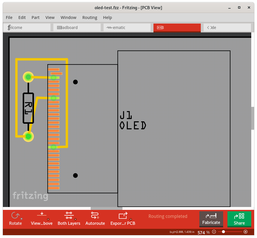
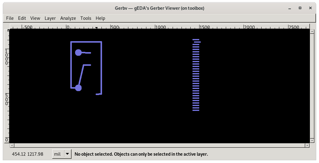
Now the shift can be seen, relative to the resistor and traces.
The problem is the svg file used for the pcb view of the part.
<svg
   xmlns:dc="http://purl.org/dc/elements/1.1/"
   xmlns:cc="http://creativecommons.org/ns#"
   xmlns:rdf="http://www.w3.org/1999/02/22-rdf-syntax-ns#"
   xmlns:svg="http://www.w3.org/2000/svg"
   xmlns="http://www.w3.org/2000/svg"
   xmlns:sodipodi="http://sodipodi.sourceforge.net/DTD/sodipodi-0.dtd"
   xmlns:inkscape="http://www.inkscape.org/namespaces/inkscape"
   viewBox="-94.5195 -1153.96892757021 1055.181 1234.70903868132"
   version="1.2"
   x="0in"
   width="1.055181in"
   height="1.23470903868132in"
   y="0in"
   id="svg90"
   sodipodi:docname="svg.pcb.OLED30v1_pcb.svg"
   inkscape:version="0.92.4 (5da689c313, 2019-01-14)">
Above is the main header for the image. It looks like pretty standard content for an Inscape file. HOWEVER, the viewBox entry is not valid for Fritzing. The -95 and -1154 values are offset to the start of the view area. Those must both be zero for Fritzing to create a proper greber export (or svg image export). The offset is seen on screen in Fritzing, but gets lost during the export.
Others here are better with Inkscape, but one way to fix this, is to use xml editor to change the first 2 numbers in the viewBox attribute to 0, then select all, resize page to selection, and save.
@vanepp The current version of FritzingCheckPart does not notice the invalid viewBox attribute value. It “looks” like all that is needed is to set the values to zero. The resize steps I used for safety did not seem to change anything additional.
I’ll have a look, I thought I had checked for non zero viewbox start, but may not have …
Peter
Having some footprint issues with some generic header parts on the PCB. For instance for a Medium (1.0mm/0.0394in) through-hole header that I then copied and used in 40 places the Gerbers didn’t provide the right hole size. For a file I have, the example above provides a drill file with a 0.038000 tool. Placing a new part and after fliping through the drop down to select Medium it does provide 0.039370, I am left wondering where this viral variation came from. Flipping through the drop down for the suspect part caused the silkscreen label to move and yes join the 0.039370 tool list. This was noticed since I was informed that the Gerbers didn’t have a hole bigger than 0.035433 when just looking at it, the PCB “clearly” has holes greater than 1mm.
For reference:
0.035433in = 0.899998mm
0.038000in = 0.965200mm
0.039370in = 0.999998mm