We are looking to use Fritzing to get our PCBs made and fully soldered with actual parts, not breakout boards, using a service such as the PCB Assembly available via Fusion PCBA.
They support many parts but for optimization prefer parts from the ShenZhen/Seeed OPL.
I looked at Aisler’s service status where Assembly is mentioned but their website seems to imply that they can only sell you a PCB, the parts, and a stencil.
To get the right footprint for the
Seeed OPL
Manufacturer’s Part Number: ABS25-32.768KHZ-T
Manufacturer: ABRACON
306010085.pdf
I started by using Inkscape 0.92.4 to ungroup the existing sparkfun part’s pads, move them, and regroup them. They disappeared due to the group name? when imported so I looked at the svg files with a text editor and it had become much more complicated. So instead, I simply hacked the pad locations and dimensions in sparkfun-freqctrl_crystal-smd-7x5_pcb.svg
using the text editor to get the right footprint as per the attached. ABS25bOSCILLATOR.fzpz (5.4 KB) It should really be an alternate package drop down - what is the correct approach for this?
Next, we tried to use the MK5P microB USB socket footprint but it doesn’t appear on the OPLs. Through hole features are stronger but Fritzing doesn’t do slots and overlapping holes might not be liked by the fabricators. Perhaps 1.1mm diameter holes will work to suit the
Seeed OPL
Manufacturer’s Part Number: 10118193-0001LF
Manufacturer: FCI
I am working on a footprint hack to try this.
The BME280 part currently is a breakout board (fine for breadboard view) and not an actual LGA. There are other LGAs in the SparkFun parts but I didn’t see one with a 2.5mmx2.5mm footprint.
ShenZhen OPL
Manufacturer’s Part Number: BME280
Manufacturer: Bosch
BST-BME280_DS001-11-844833.pdf
Thank you for your follow-up. I do understand that parts have a linked (with hopefully accurate labels) breadboard image (looks like the part with connectors in the right places), schematic image (right number of connectors), and pcb image (dimensionally accurate). The drop down “functionality” is not clear to me yet.
The drop downs that show in the Inspector window for a part? For “normal” parts (not core library “factory” parts), This provides a way to switch between parts in the same “family” that have different values for the properties defined in the current part.
You mentioned connector linkages between views. That is done in the part definition (fzp) file, separate from the svg image files. In there, each connector for the part is defined, with an “svgId” for each view that points to the connector element in each svg file. The names can be different in each view, as long as the fzp file points to the right name for each view. It can be confusing if the “numbers” do not match, so don’t do that. The names are often slightly different. connector0pad in pcb view, connector0pin and connector0terminal in schematic view, connector0pin and sometimes connector0leg in breadboard view.
The fzp file also contains “property” information. I mentioned family earlier. There are a few special properties (like part number), but in general, each property in the fzp will become an entry in the Inspector, and the entry will become a drop down if there is any other part (either user part in a bin, or core library part) with the same family name and property. So if 2 separate parts have the same family, and each have a (different) size property, a drop down will be created, and changing the drop down value to the other size changes the part in the sketch.
So you want to create properties where the value for the current part could be different from the value for a similar (family) part. The combination of property names and values needs to be unique from all other parts in the same family. Package is an example of that. 2 otherwise identical parts in different packages can be swapped between, if they are in the same family, and each has a package property.
I certainly find the behaviour of having three drop down Properties say variant, target, and package, all change when one is changed for a chosen part challenging.
I’ve also recently tried to understand the following.
Fritzing->CORE->Basic->Mystery Part
rotate/flip in schematic view resave/open
lettering on part appears in new place, sometimes part appears in new place without connections but wiring reconnects when part dragged.
Alternative approach:
Fritzing->CORE->Connection->Generic Header
Place and select a form other than shrouded.
The multiple changing drop down values when a single one was actually changed, is because not all combinations of property values exist in the available parts. What is offered on the drop down is (I believe) all of the values that can be found for that particular property name, in the current part family. This is done for each property name in the current part. When a single property is changed using that list, Fritzing then looks at all of the available parts in the current family that have the selected property value, picks the one that most closely matches the rest of the property value for the starting part. “most closely” can be “not very close” depending on the particular parts. The logic for “most closely” is also not at all clear/published. If it is anything like the autorouting logic, it could use some improvement. Once the new part has been selected, all of the property names and values are updated to match the new part.
The substitution only works the way you want (expect) when there is another part that has all of the same property names and values as the current part, except for the property value that is being changed. In all other cases, other property values are going to change as well, and quite possibly property names.
The movement of the labeling on rotate and flip is a bug that has been reported. It is on the list to fix, along with many others, and very limited resources to work on them.
When a part is flipped or rotated, it often does not end up with the connectors aligned to the current grid. The part needs to be dragged slightly to get it (and the wires) to snap back to the grid. I have not seen parts jumping after save and open though.
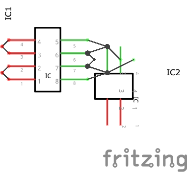
Not that there’s a 3 pin option but I was able to duplicate the save and open issue with the generic IC:
Good to hear that someone has reported a related bug properly. I suspect the xml storing the location and that the part is flipped and rotated is stored but that the “drag” to reconnect/redraw has been hacked to be stored in some way that doesn’t always work.
I also noticed that the hole size Extra option provides a design rule breaking footprint unless you reduce the advanced settings Ring Thickness.
And of course, as mentioned choose one package down accidentally (LQFP) and though you can choose a number of different options in the new variant drop down that change the package and connectors drop downs, you have to go back to the package drop down to get back to DIP. Based on the explanation I could imagine a path where clicking a part’s dropdowns will get you into a loop where one change cannot get you back to say DIP without at least two informed sequential selections.
From your description, without even looking at the part.
The through hole connectors need to be on BOTH copper1 and copper0 layers. If I understand what you are doing, the way to get there is to have the copper0 layer (group) inside of the copper1 group. The SMD pads go on copper1, outside of the copper0 group. The through hole connectors go in the copper0 group, which also puts them on copper1. From where your description puts things, the fix should be as simple as moving the copper0 group (and all of its content) into (inside) the copper1 group.
I noticed mistakes with my copper0 tags which I fixed but then when I imported the image into the part again there was no change. The copper0 is indeed in the copper1. I am trying to upload just the svg and I am getting “Sorry, but we couldn’t determine the size of the image. Maybe your image is corrupted?” I will open and re-save with inkscape.
Resaving it didn’t work, then tried to upload from fritzing.0.9.4.64.pc\fritzing-parts\svg\core\pcb
and the following sampling got the same message:
5mm_LED.svg
SMD_0603.svg
sparkfun-led_led5mm_pcb.svg
sparkfun-discretesemi_0603-res_pcb.svg
The “can not determine size” happens a lot on the forum with svg images of parts. Especially small parts. The actual part (and svg unit) dimensions tend to be down around (and less than) 1 in, which the forum software does not think is big enough to be a “real” image.
I have gotten around that a couple of different ways. Change the height and width values on the svg header element to something bigger. Like 10 times bigger has always worked. As long as someone does not try to use the image as is to create a part. Another way is to add something to the image (bottom right) to make the dimensions bigger. I think you can also put the svg in a zip file, renamed to .fzpz, and upload that. Whatever method you use, be sure to include the details so we know how to get back to the actual svg file.
EDIT:
I ran the originally posted part through FritzingCheckPart. It said that was an smd part, because only copper1 view is present. That is in the fzp (part definition) file. Examining the fzp file finds only copper1 references, no copper0. For a part with both smd and tht connectors, the pcbView needs to include both copper0 and copper1 layerIDs, then the individual connectors need to have one or both depending on the individual connector. With no reference to copper0 in the fzp file, the copper0 group in the svg is going to be ignored. When the copper0 is inside copper1, the content is going to be seen as ONLY on the copper1 layer.
FCP also shows that you have silkscreen content that is color #f0f0f0. That should be either white or black. The current style uses black. That is actually a mask for where the silkscreen exists, not the color it is supposed to be.
There are also a couple of warnings about schematic view terminals with zero width, that can cause problems if svg is (later) modified with Inkscape. Connector numbers (id in the fzp) should start at zero, and be in ascending sequence. The pcb silkscreen layer should be before the copper layers, to make selection in Fritzing easier.
It sounds like you are trying to do both through hole and smd in the parts editor which won’t work. You have to manually edit the underlying files. A description how is available here:
@vanepp Your instructions use duplicate connector pin ids on separate copper0 and copper1 layers. Did you try putting one layer in the other, but only including the THT subset in inner layer? Conceptually that should work. Real world, maybe not.
That of course will not work when mixed with edge ‘fingers’ that have smd pads on top and bottom for different connectors. For that, the copper0 and copper1 groups need to be separate. Or duplicate the inner group to make it also distinct. Which would again break Inkscape, but if Fritzing allows it, changing a “copper0a” id to “copper0” would be a one line (one character) change after finished with Inkscape.
<g id="copper1">
  «smd connectors that are only on the top»
  <g id="copper0">
    «through hole connectors»
  </g>
</g>
<g id="copper0">
  «smd connectors that are only on the bottom»
</g>
I based the footprint hack (moving pads and trying to add through holes) on sparkfun-connectors_usb-ab-micro-smd_pcb.svg (SparkFun-Connectors->USB_AB) and it seems I may actually have to change something more than just the svg to get through hole attributes (two plated through holes that will only be mechanical) and loading the image in the PCB tab of the Parts Editor. When I do that, View->Copper Bottom Layer only, the nested group0 doesn’t appear on the bottom. I went to the Connectors tab of the Parts Editor and selected Through-hole. It seems to do what I needed and may be workable, it also creates a joined terminal on the bottom layer of the through holes to D+. I moved the silkscreen group above the copper1 group to make it easier to select copper, I hadn’t been selecting anything (I kept the same ids). Reassigning D+ the bottom layer disappears again. When trying to Ctrl click to re-assign the through-hole to D+ it doesn’t end up back to where we were. Clicking SMD then Through-hole again also adds the pads to the bottom layer which I don’t want. My changes in the Parts Editor seemed to have propagated to the file I saved earlier that had a workable set up. I have been trying to click on the tick-boxes in the Connectors Tab of the Parts Editor to get the behaviour that I want and thinking about making the through-holes unused connectors but I think it is time to look at the corresponding xml. I still wonder about my svg. Since uploading an actual working svg may not work on this forum, I will try the xml as code (inMarkDown tags: ‘’‘xml code ‘’’ where the 's are actually back ticks):
I think so. I had not realized that the through holes were mechanical, not actual connectors. But I expect that the fzp file needs changing, to tell it that both top and bottom are to be used.
I do not know if parts editor will let you do that without also changing the connector pads to through hole. You might need to adjust the fzp after saving it from parts editor. The fzpz file is just a zip, so can be unpacked, edit the .fzp, zip again.
The silkscreen graphics should use black, not F0F0F0.
I did note that when a design has the part, upon opening the design, the copper bottom is randomly assigned to one of the five USB pins. It doesn’t matter to me since I am not making any electrical connections to it but perhaps it should be tied to ground. I suspect it is because every connector in the fzp is specified as: