Request: Dragino LoRa Shield for Arduino

Hi! I am new to the fritzing community, but I need this shield part for an installation guide I am making for my thesis…

I found the below image with the part on the right, but no parts files. Does anyone have this shield part or know how to build it?

Also: Would it be possible to have a part that could just snap on top of an Arduino?
I hope you can help!

Thanks,
Simone

Update: I’ve found a simple version of the part, but it is too big for some reason, and gives the warning that there are ‘77 unassigned connectors over 2 views’ when exiting the parts editor. Does anyone know how to fix this and the size?
Dragino LoRa Shield V1.4.fzpz (46.5 KB)

Update 2:

I have attempted to resize the breadboard and pcb files like described in this post, so they should be the right size now.

I am not really a hardware person, but it seems to me that the schematic file does not belong to this part? I don’t know if this will be an issue as I am only looking to make a wiring diagram for an assembly guide.

Aaaand: it worked! Somewhat. The sizing is still a bit off. It should still work for the purpose, though. Here is the result (on top of an arduino uno):
image

Not really worth uploading, but here it is anyway: Dragino LoRa Shield V1.4.fzpz (54.6 KB)

Welcome aboard!

Almost, but the connectors were a bit uneven, and needed some adjusting to be exactly on .1in boundaries. A number of the pins also are not configured, I’ll dig up the docs on this and add them to the files.

You are correct, schematic looks to be for the part this was cloned from, not this board. I’ll fix that up too (haven’t yet though.)

Good call! While I could started from the original this one easier to fix :slight_smile:

Yes (with some limitations due to bugs). Your original part won’t do it because it has female pins as does the Arduino and probably the pins were not aligned closely enough. In this breadboard image (with my part) we see that Fritzing looks to have aligned the shield with the DiO0 header, that means the connections to the Uno (circled in blue at the top left) are slightly offset, just enough that they won’t connect. You will also see the Arduino connectors are dark and the shield connectors have (currently) a red ring around them (indicating no connection). The Arduino pins are female (like a breadboard) and the shield connectors are male. To get a connection you need female to male (or a wire which will connect to either.) The two sets of pins outlined in blue are not defined as connectors in Fritzing, to make it most useful they should be (I’ll do that later.)

Here is pcb view of the above sketch. The uno is on the top and the shield on the bottom. No connections because there are non in breadboard. The undefined pins are circled in red here.

Now to fix the alignment issue in breadboard so the shield will connect correctly. To do so you need to turn either turn off snap to grid (which is what I did) or set the grid size small enough that you can align the pins. For this I clicked View->Align to grid to disable the align to grid function then dragged the shield til the shield connectors aligned with the Arduino connectors:

If you look at the SCL connector (outlined in blue) you will see the red outline is now green indicating a connection. At the bottom of the screen you will see the result of a bug. That should say routing complete rather than 0 of 27nets routed. Switching to pcb we see the connections between the shield and the Uno have been made (the rats nest lines reflect connections in breadboard and schematic if it was working):

Here is the updated part that you can play with and I will work on fixing schematic and adding the missing connectors.

Dragino LoRa Shield V1.4-1.fzpz (34.2 KB)

Peter

1 Like

OK a bit late, but here is a full part for this. I decided this would be a good example for an Arduino shield template document, and so upgraded this part to meet the standards for inclusion in core (pcb was slightly out of scale, possibly due to different Inkscape versions.) Schematic is formatted suitable for a yet to be done shield friendly Arduino part (the current part in core lacks ICSP1 and ICSP2 connections and this shield is using ICSP1 …), that is next to be done. Assuming you have one of these boards it would be very helpful if you could print out the pcb view at 1:1 scale and see if it matches the board (it should for the Arduino pins, but I’m less sure about the various jumpers. but hopefully they are in the correct place too!)

edit: I found the breadboard ICSP connector was offset 0.012in in X in the original part, just enough to cause it to not connect to the Arduino in breadboard. I have corrected that and updated the part, so if you have downloaded it, please download it again!

Dragino LoRa Shield V1.4.fzpz (17.0 KB)

Peter

1 Like

Here is a new Arduino R3 variant, which has a shield friendly schematic and no pcb view.

Arduino_uno_Rev3-shield-schematic-no-pcb.fzpz (28.1 KB)

The intent (if not currently due to bugs, the practice) is this: in breadboard the Lora shield above (with the grid size set to 0.01in so the parts will align properly) and dragged over the Arduino connections as it would be in real life, connect the Arduino to the shield:

Note all the Arduino connectors (circled in blue) are green, indicating connections on all pins. That should produce this in schematic (in practice this was produced by connecting all the pins with wires!):

The Arduino on the left connects to the shield on the right (and the Arduino doesn’t appear in pcb, only the shield). Unfortunately we appear to have bugs so the actual schematic from the above breadboard connection looks like this:

The missing wires (circled in red) show up as rats nest lines elsewhere (circled in blue) except for the two grounds which are missing entirely. Attempting to make a connection across the two pins (such as the ground) fails (which it should not.) I will report this as a bug on github and when it gets fixed, this can become the new shield template. For anyone that wants to poke at this here are the two test sketches that created the above images:

Correct-connection-by-wires-Sketch.fzz (64.8 KB)

Incorrect-connections-by-overlay-shield-on-arduino-Sketch.fzz (52.8 KB)

Peter

1 Like

Wow, thank you so much for all your work, Peter!!

Really great :smiley: Will be perfect for my diagrams!

Simone

I’ve been intending to fix up the core Arduino parts for a while and create one that was shield friendly, this was a good excuse :slight_smile: , if I can now get the bugs fixed life should improve!

Peter

@vanepp

Peter you are simply awesome! You do such great work, love how you help others. As I stroll threw, tidying up. I can’t help but notice. A natural leader by example. Excellent work! Thank you very much for all your hard work, we can never say it enough. We can’t do it without good hearted individuals such as yourself. Soooo, thank you again!!

Stay safe! Watch out for the invisible enemy… :upside_down_face: :wink:

1 Like

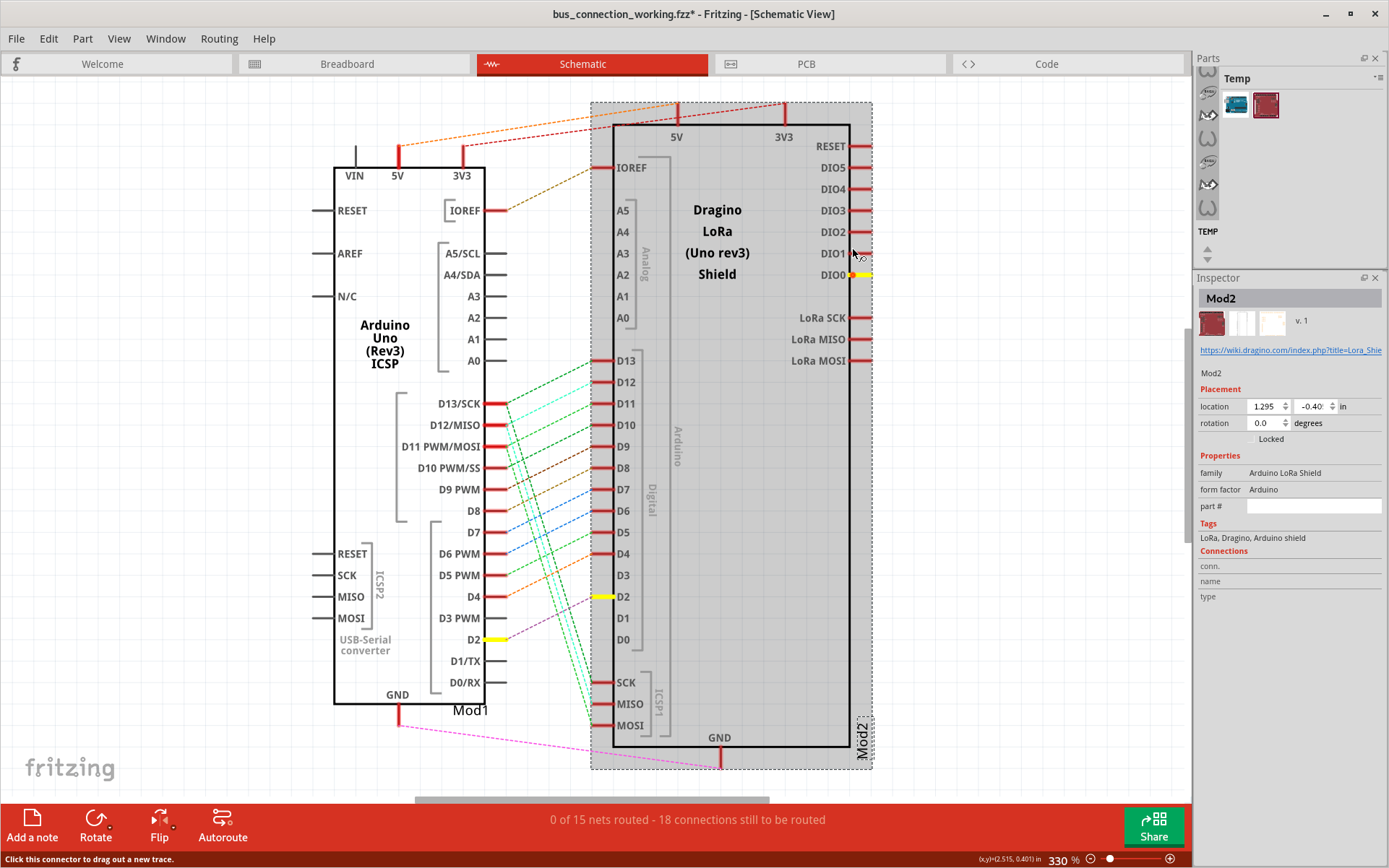
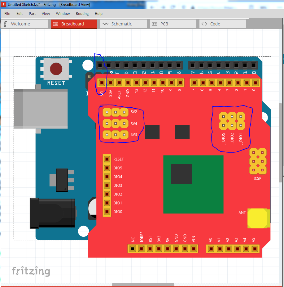
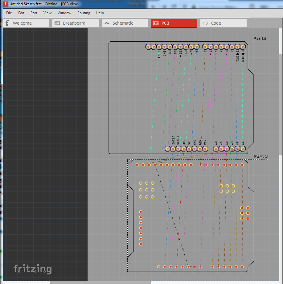
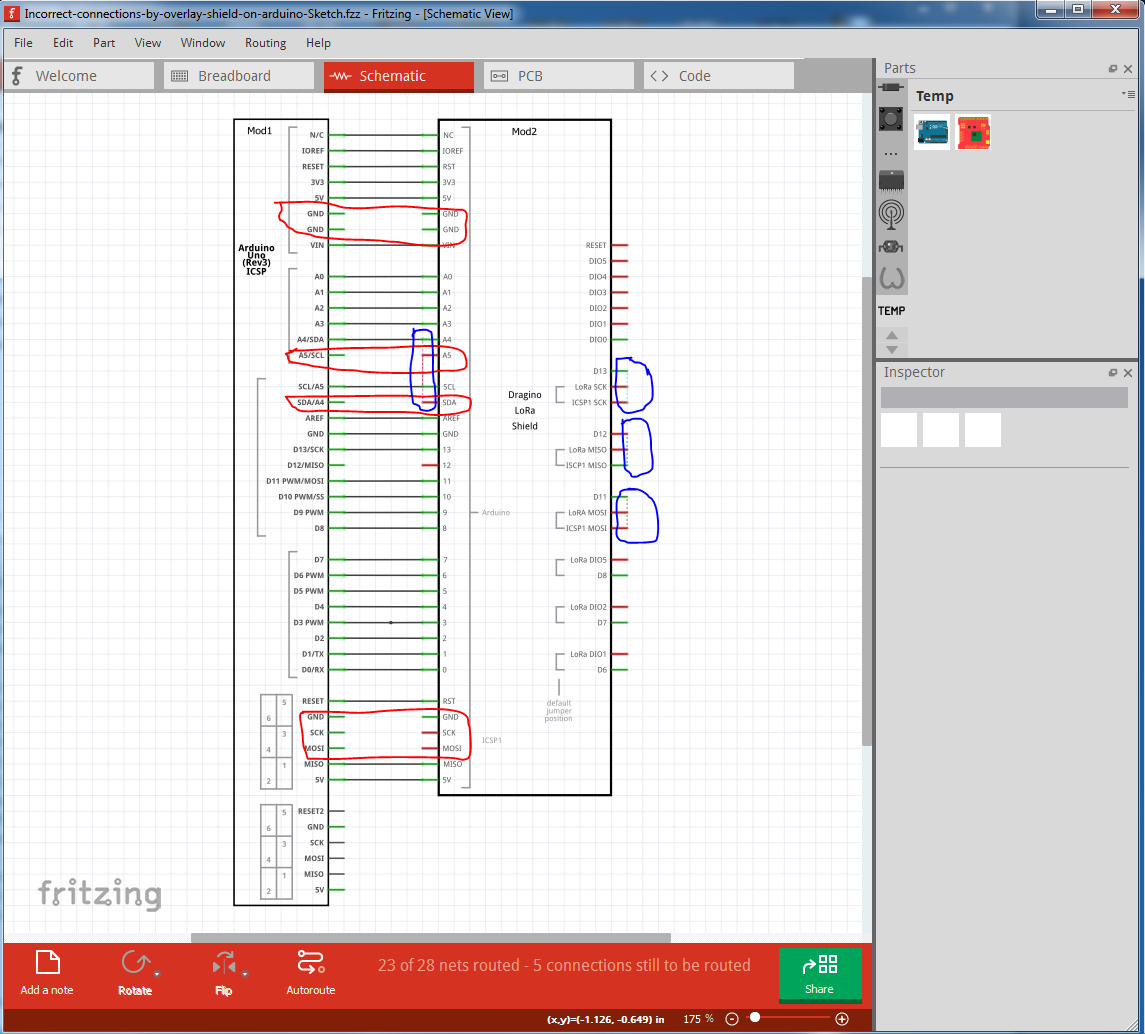
@vanepp After going over issue parts with grouped pins don’t connect correctly in schematic, doing some research and exploration, I think most of the issue seen here is “works as designed”. Bused connections (pins) are effectively a single wire, and the schematic ratsnest will (and should) only connect one wire from one group to another. That covers the missing GND wires. For the other, visually miss-placed ratsnest wires, the schematic is a logical view, and does not know anything about the physical positioning. It just looks for the shortest way to connect 2 (groups of) pins together. So, with the parts positioned as shown, it is shorter to draw a ratsnest from shield pin “D13” to shield pin “ICSP2 SCK” than from Arduino “SCK” to shield “SCK”. Those are electrically (logically) equivalent wires, because shield pin “SCK” is internally connected (bused) to shield “ICSP2 SCK”. However, that “shortest path” changes based on the position of the parts. Deleting all of the wires on the schematic view, and moving the parts closer together (less than 0.2 in between the ends of the matching pins) moves all of the ratsnest wires to straight Arduino pin to shield pin. Once the short ratsnest wires are replaced by real wires on the schematic, the parts can be moved apart again, and everything (except the multiple GND pins) will be as expected.

shield-schemtic
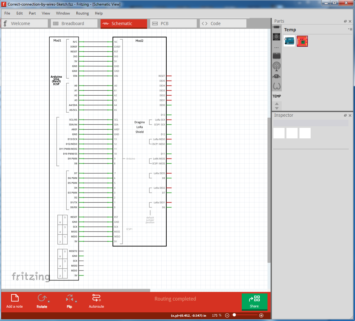
correct-connections-by-overlay-shield-on-arduino-Sketch.fzz (49.0 KB)

There is still one bug outstanding, and a bit further documented in the referenced issue. That means the parts needed to be moved so that the automatically placed ratsnest wire goes where you want it, then create the real wire for it, then move the parts again to where they are really wanted. Instead of simply ignoring the ratsnest wire, and connecting where you want on the same bus.

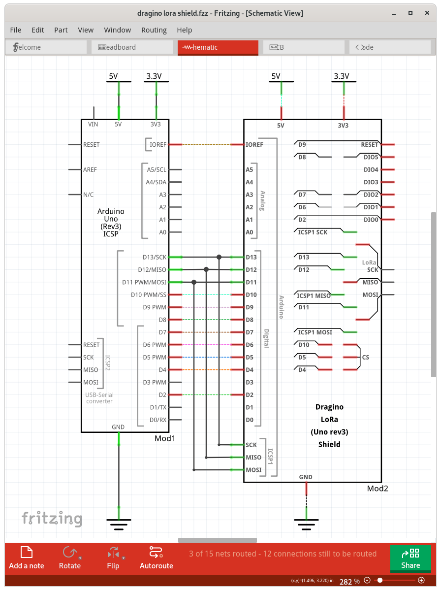
Personally, I would change both parts to have a single GND pin at the bottom of the schematic, and wire each of them to a ground symbol, instead of to each other. Same for VIN, 3V3, 5V. Put a single one of each of those at the top of the schematic block, then connect to matching VCC symbols instead of to each other.

I would also leave out any pins on the shield that are not really used. If they are only used to pass signals through to the next stacked shield, they are not needed on the schematic. They have no logical function.

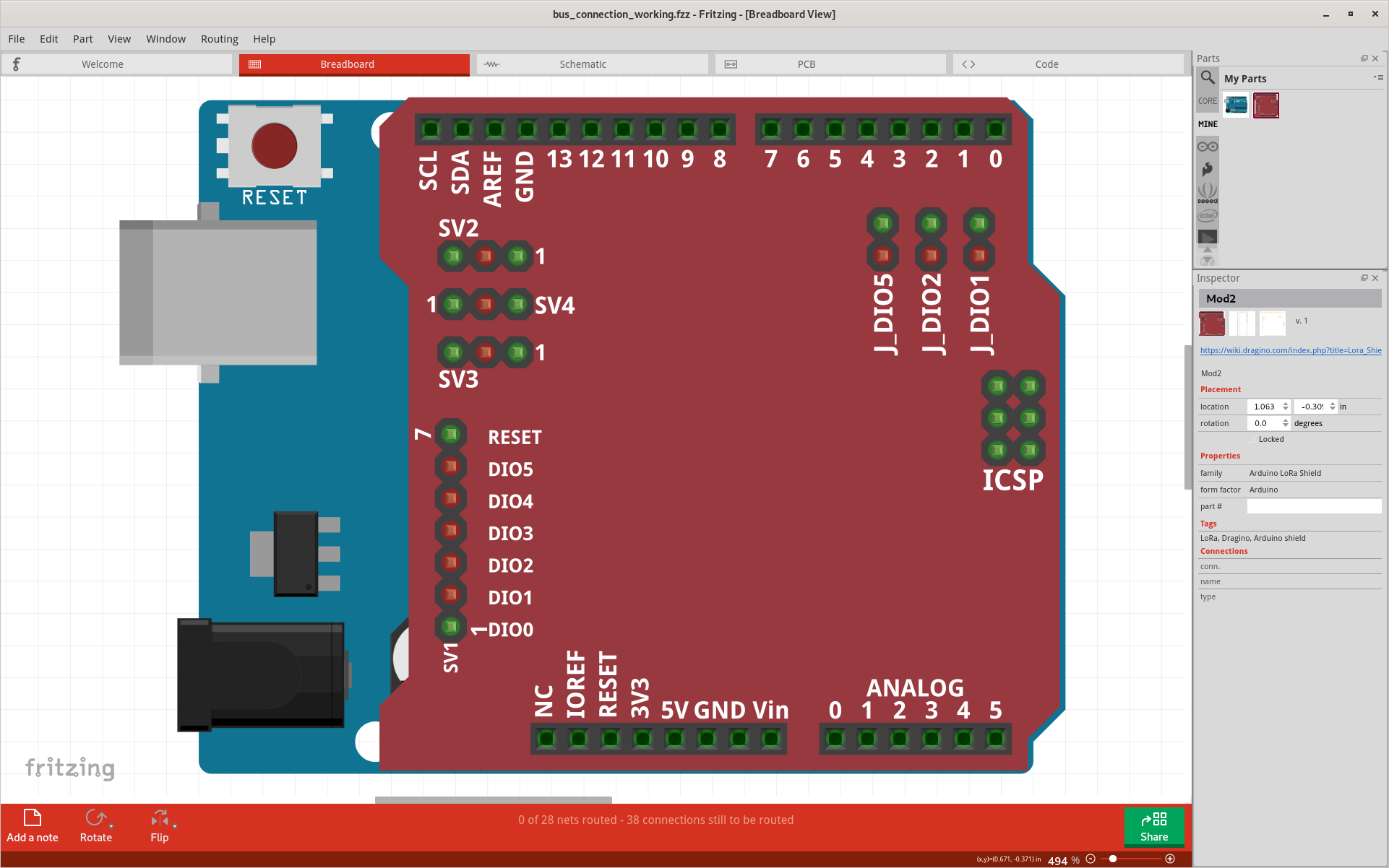
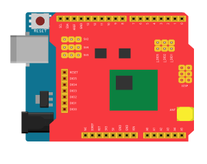
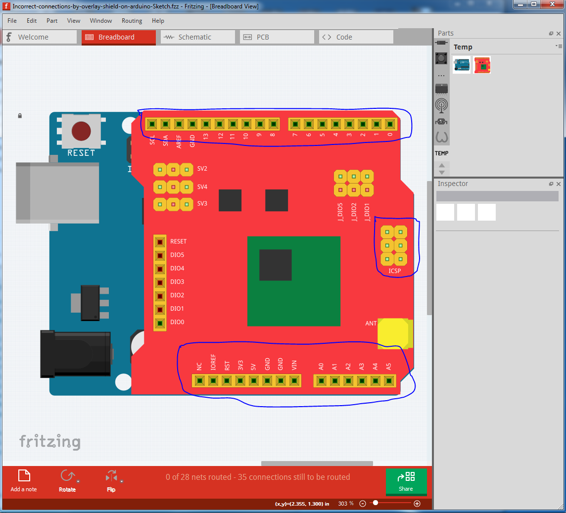
A (functional) block of pins on the Arduino for ICSP makes sense, but there is really no need for 2 of them (on the schematic). Internally the pins are connected together, so one set (without the common GND) would be enough. Also, is the 5V pin for the ICSP internally connected to the (outer row) Arduino 5V? If so, those should be bused, and are not needed in the ICSP block. Probably the ICSP block (group) of pins should only be SCK, MOSI, MISO. Those are the “functional” pins.

I can see the truth in that, but at the same time, you can (should may be another matter though :slight_smile: ) do this in the real world and in my view should be able to in Fritzing too (although being able to do so from a code point of view may be too expensive to consider.)

I agree with that, and normally (with non bused connections to a bused connection such as ground) the same thing happens, the rats nest is in the wrong place but you can “correct” it by manually routing the wire where you want it. With both connections in a bus, you don’t appear to be able to do that (and as noted it may be too expensive code wise to allow it.)

That may end up being what has to happen, due to how the code works (and the work required to change it), but I would rather see if we can fix it reasonable easily. What I’m interested in here is seeing if we can make this simpler for folks new to schematic and/or electronics in general. This same issue came up in the Calliope board that I was fixing up for a group or educators, I proposed a schematic similar to this one where schematic matched breadboard which to me seems easier to understand if you aren’t already familiar with schematics, but in the end they decided schematic was supposed to be more abstract and decided the original way was better (to me it seemed less intuitive, but it was their project.) My aim is usually for maximum laziness, understanding with minimal thinking, and that is what I’m trying to achieve here.

For the shield side, that is fine in some sense (although I’d probably like to know of connections that just pass through as well,) but for the arduino side all the possible connections need to be there so any possible shield configuration can be represented, because we only want one “shield friendly schematic configuration” part not many of them is my thinking.

As far as I can see that isn’t true. The second ICSP connection appears to connect not to the Arduino’s 328 CPU as the first one does, but rather to the USB processor cpu, so for completeness (in case a shield needs to access that ICSP for some reason) the pins need to be at least on the Arduino shield friendly schematic version of the part (although not used in this instance.) As noted I’m trying to make a single “shield friendly” Arduino schematic that will apply to any shield configuration to prevent a part variant explosion (which wasn’t articulated in this post before.)

Peter

You currently can do it, in the breadboard and pcb views. However, schematic view is very much not (does not need to be) real world. It shows logical connections, not physical wires or traces. 2 wires connecting the same 2 points do not make any sense. For a logical connection view.

Currently you cant directly do that. Which is the (real) bug here. You can do it indirectly as shown in the example I included.

Pass through to where? The UNO schematic would still have the (unused by shield) pin, so if something (another shield, or direct connect) was using it, it would (and should) connect there, not to (through) an otherwise unused pin on the shield. Logical view again, not real world.

Sure. But each shield only needs the pins that it uses. The shield schematic graphic can either leave gaps for unused pins, to get the wires straight, or collapse the holes and route the wires a bit.

So ICSP2 pins are NOT tied to ICSP1. Which, yes, means they need to be included separately on the schematic. In fact, that would be an opportunity to do a split part, so that the (logically unrelated) usb serial conversion pins could be moved around on the schematic. Though I did a bug report (Fritzing 0.9.2b I think) about problems using bus and spliting in the same part. (I tried to do a DPDT relay where the schematic switch blocks could be moved to where they were logically used)

That was understood. Shield friendly does not mean that duplicate (bused) Arduino pins have to be included multiple times in the schematic view. The shield(s) only need a single copy of the same pin(s). Tweaking the (shield) pin labeling can show how the shield sees that specific pin (D13 versus SCK). I did say that a separate ICSP (1) block made sense, so for cosmetic reasons, the shield graphic could position that pin where it will align cleanly with either D13 or SCK in the ICSP block. If it using the pin for SPI, align with the ICSP block. If it is using it for general data, align with D13. But probably do not need both of those on the shield. Or either, if the shield is not using that at all.

I’m working on variant UNO and LoRa shield parts to demonstrate what I mean, but I am not as fast at part creation as you are. Not that my version will be “right”. Only showing that there are other ways of looking at and solving the same problem.

@vanepp I finally have a pair of reasonably functional (still incomplete) parts for demonstration. Also for discussion on bugs and limitations. I think that should go into a thread on fritzing-app issues. It is a lot more code related than parts creation. Before starting documentation and categorizing of related bugs though, could you have a close look at the parts? See if I did something wrong/different/non-standard that could be impacting the functionality. And perceived bugs.

I am including a sample sketch setup similar to the earlier sample here, along with separate parts files. The shield is placed over the Uno in breadboard view, connecting the matching pins.

I found an issue with that. It seemed like each time I recreated one one the parts, Fritzing chose a random connection to base the align to grid on. Only rarely could I get the parts to connect when align to grid was turned on. One non-standard thing I have, is blocks of definitions in the fsp file commented out. Things that are not needed yet, but intended either for use later, or for documentation. FritzingCheckPart warns about them (multiple times), but they should be valid for xml.

In schematic view, I added minimal extra power connections and wires. Just enough to get the ratsnest wires to go reasonable directions. pcb view should be standard. Assuming the parts themselves checkout valid, things to discuss are where it should be possible to add a real wire, and where Fritzing shows existing connections. What it highlights when mouse held down on a connection. Which is different in each view. I am seeing some unexpected cases, but want other part builder eyes on the parts before pointing and saying bug.

shield test.fzz (39.7 KB)
arduino_uno_for_shields.fzpz (27.2 KB) dragino_lora_shield.fzpz (9.6 KB)

The parts both look fine to me, the pin numbers are not in sequence (probably from the Uno which uses the eagle2Fritzing numbering which also isn’t in sequence.) I have seen that (usually in parts with schematic subparts) cause errors when hovering over pins but that is about all. I can convert them to in sequence, but the process will ungroup every thing and lose your formatting and comments. Or it can be done manually (but that is painful!) I’d say you are pretty much good to go.

Yep, comments are being mistaken as unrecognized spice data and thus the warnings. I added a filter for comments that just silently discards them.

Peter

@vanepp I created an issue for a code bug from this. If interested, see the details.

The sketch file, and embedded parts, over there are slightly different than here. I found a bug in the shield definition. The ICSP header bus definitions were missing. Getting this fixed may fix all, or only part of the bugs talked about earlier in this thread. As opposed to the working, but not quite as expected/desired. I need to expand my example shield part some more to test out using the headers to switch the LoRa ICSP connections, and getting the manually placed wire were desired instead of where the ratsnest defaults to. The work around of moving the part to get the right ratsnest line first may be all that is needed, but I am suspicious there may be another problem in there. Possibly covered by Fritzing not completely handling the bused connections across views, but maybe not.

I also want to explore options for showing and using the jumper header pins in different views. Considering using internal connector pins in schematic view (inside the body of the part graphics, instead of at the outside edge). Those do not normally go anywhere except to another (physical) pin on the same part, so internal open/closed shorting jumper should work. If I can get a clean way to lay it out.

The existing example should be enough to show what I was talking about earlier in the thread, about an alternate way to layout the schematic view of the parts, using the top and bottom location for power and ground, and only including pins for the shield where the shield electronics actually connects to them. Labels of unused pins (pin location) are optional, but since need to leave a gap anyway, to lineup with the ‘standard’ uno (or other board), I figured they might as well be included. Besides, I built a shield template part in the process of this, and all of the normal uno footprint pins are included in that. Easier to delete unneeded pieces than to add them back in each time.

I

Reading carefully what slack is telling me, I think you have all slack notifications turned off, so, unless you login there occasionally, you have not seen the messages I sent to you there.

That wasn’t intentional! I’ll log on and see if I can correct that :slight_smile: . That may explain why I haven’t seen any activity lately.

edit:

My connection is in such bad shape (around 1% packet loss 100ms - 2 sec ping response to first gateway) that the slack login won’t complete. I expect it times out due to the slow connection. So slack may need to wait for a new network connection …

Peter

I’ll have a look (Internet connection willing) and comment there. Thanks!

Peter

Here is a version of the example sketch with updated parts. I found a way to get the effect I wanted with bused connectors.

Still need to implement the configuration jumper headers the way I want for schematic, but making progress.

bus_connection_working.fzz (38.8 KB)


Here is what should be a fully functional version of the shield friendly uno and Dragiono LoRa parts. Bugs allowing. I did not fill in the shield breadboard graphics beyond what was useful for identifying the functional parts. The focus was on getting the schematic view layout into what (to me) was a more logical structure. Inputs to the shield (the Arduino pins) on the left, power and ground top and bottom, shield specific IO on the right. No duplication of bused connections, no connections on the shield for pins that are never used (directly) by the shield. After some iterations, I found a reasonably clean way of showing the shield configuration / settings jumpers internal to the main schematic symbol block. Both sketch and part files included, so you do not need to extract from the sketch. To get the schematic to work this way, with the LoRa ICSP as a output, I needed to duplicate (and bus) the connections for use with the internal configuration connections.

dragino lora shield.fzz (42.0 KB)
arduino_uno_for_shields.fzpz (27.5 KB)
dragino_lora_shield.fzpz (10.4 KB)

Here is an image of the schematic view with (just) enough real wires to get the rest of the ratsnest wires to go to reasonable locations.

Discussion open for this style of doing the layout.