I’ve been trying to sort this out for 3 days, now, but to no avail.
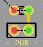
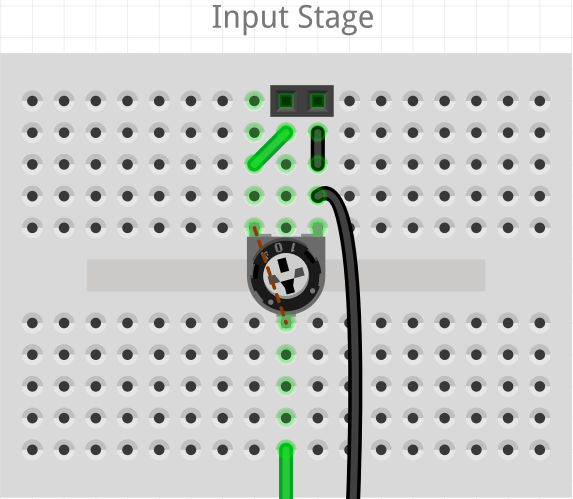
I’m getting a ratnest line from 1 leg of a trimmer/potentiometer to the wiper (going through the potentiometer). This is on breadboard, schematic and pcb views.
Getting ratsnest lines between the pins of a 2-pin female header and through the middle of a capacitor on both schematic and pcb views.
I was able to get rid of most of them on the right hand side by picking up parts in BB view, moving them away and back.
Try to avoid parts on parts or wires on parts, ie see the green wire on the cap top right, it’s probably not connected, put the wire in front of the cap.
I was left with the VR and PWR+1 header rats, which I couldn’t delete, so I duplicated them, deleted the originals, and moved the duplicates into place.
Thanks, Old_Grey. I managed to get most removed as well.
It appears, when in BB view, if one shortens the legs of a component (the cap top right), they have to zoom in real close and make sure the ends of the legs actually make connection to the breadboard holes.
As per your advice, I completely removed the components and replaced them with ‘new’ ones. All worked then, except for that pesky trimmer/potentiometer. It still has the ratnest line going through it, even after being replaced. When I delete the line in schematic view, Fritzing shows routing complete. But then in BB view, the trimmer has been moved completely off the breadboard and has wires attached to it. I deleted the wires, moved it back on the breadboard, and that pesky line showed up again. Also the wiring for it in schematic view was lost. I redid that wiring, and the line showed up again there !
Ok. Thanks. I’ll be happy to give it a try and report back to you !!
However, I’m seeing ratnest lines that make no sense on other sketches as well (like in between the pins on 2-pin headers).
As mentioned earlier, at times schematic view will show “routing complete”, but breadboard and pcb views show ratnest lines and report that connections need to be made. It appears to me the 3 views are not correctly updating with each other.
Your problem with the pot appears to be a disagreement between where you think the pins in breadboard are and the pin numbers in schematic. If you select the two green wires on the pot in breadboard and right click and delete wire you will find that the rats nest is in fact the opposite direction to how you have the connections made. While it will let you make the connections you have it also then made a short (and the phantom rats nest lines) between the two pins of the pot which isn’t what you want. It also now appears to remember the rats nest wires (which is likely a bug) so that the rats nest is still incorrect. Presumably that is why the duplicate / replace fixes the problem. If from your initial sketch, you delete the two green wires on the pot and then make the connections in breadboard following the rats nest connections (which will be a different physical layout than your current setup) the phantom rats nest lines will go away. I assume (but haven’t checked) the other problems have a similar cure. Connections made in on view reflect in to the other two views so a mistake in one view can cause odd problems like this.
Folks… I’ve tried this again with a less complex circuit.
It is quite clear to me that the 3 views and ratnest lines across the 3 views in Fritzing simply cannot be believed.
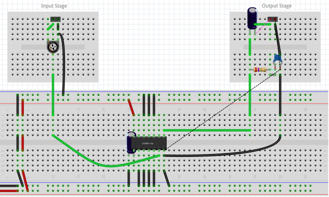
This one is an LM386 Audio Amp.
I started this one with the Schematic View. Got “Routing completed”.
Then went to PCB View… Routed Traces… Got “Routing completed”.
Double-checked Schematic View… Still had “Routing completed”.
Then wired up Breadboard View… Got “Routing completed”.
GREAT ! DONE !!! NO !!!
Both Schematic and PCB views now show 6 Connections still to be routed ! Nothing was changed in those views ! Those views now show ratnest lines where there were none, and show them in places where they shouldn’t be. The 3 views simply don’t agree with each other. This basically renders the software non-functional.
Here is the sketch. Each view has the original schematic I’m working from.
Can someone please explain what’s going on ? Ruby.fzz (966.0 KB)
While I probably haven’t found all the problems yet, one immediate one is that you have swapped c1 and c2 on the insert schematics. In the Fritz schematic c2 is 47nf and is the coupling capacitor to the volume control, in the inset schematic that is c1 and c2 is the power filter cap. In breadboard c2 is the 47nf ceramic connected to the volume control and the source of the fet as it should be and c1 is the power supply cap. On pcb c2 is across the power supply causing the extra rats nest lines and various shorts (as that is also how the copper is routed) and c2 is connected as the source coupling capacitor. So the rats nest lines are likely in the correct place (although there does appear to be a Fritzing bug as well because if you eliminate all the connections the rats nest lines remain …). I’ll poke at this some more tomorrow.
Sorry… Misstated that. I placed the bypass cap on the power supply 1st.[quote=“vanepp, post:12, topic:2652”]
causing the extra rats nest lines and various shorts
[/quote]
There are no shorts. If there were, one could click on either + or - on the breadboard power rails and both would light up.
Leaves me wondering exactly which view is Fz using to determine its ratnest line placement. As I stated, I started with schematic view. I then expected ratnest in PCB. But those 2 views agreed with each other when I laid down the traces. BB view is what’s throwing the others off.
And also, why are ratnest lines showing across the IC pins in schematic view when there are clearly no connections there on any of the 3 views ?
I think it’s the way you are working. It seems that you do one view that isn’t 100%, and then you try to fix it in another view when you should be fixing it in the first view. If you have the SCH just duplicate it exactly in the SCH view and make sure it’s right, ie no red ends, grab junctions and move them and make sure all the wires go with it, etc - your C1 isn’t connected to VCC -. If you have the SCH view you don’t need the BB view so don’t even bother laying it out.
I bet if you opened a new window and copied every thing in the SCH view and got it right, I bet it will be right in the other views. There is something in FZ that it’s best not to do something in one view and fix it in another view.
I guy did this board with maybe 100 components and it was fine.
Old_Grey… I really appreciate your time looking at this.
That is not a correct assumption.
Yes, C1 is connected to VCC -. I set up the BB, SCH and PCB views and saved it as a starting point for all sketches (so I wouldn’t have to keep redoing them). You may be referring to the PCB view. It’s only the label for the 2-pin input header in that view that needed flipped (the pin numbers for that header are consistent across all views).
As I stated, both SCH and PCB agreed with each other until I laid out the BB view. I kinda agree with you on not messing with BB view, as it is the one that threw the other two off, but then there would be no reference to test the circuit before any soldering took place. To me, that’s a bug in the software.
Also, try this…
In SCH view, delete a rat nest line (if Fz will let you). Then look at BB view. Fz throws the component completely off the breadboard and connects it with wires… Even if you have the component ‘locked’ in that view. Why ?? That is a problem.
In SCH view, whenever you have a 3 way junction you should have a big dot, like on the GND side of C1. If you look at the positive side it has a small dot, so it’s not connected. It looks like VCC was connected to something, and then one side of the wire after the bendpoint was deleted. There is a hint when you join to a bendpoint, because snap turns off for that joint so you have ti reposition it, and that’s when you notice all 3 are connected.
Let me have a play and I’ll see if I can find something.
I had to delete all the wires from all the views, relink the SCH back up again, and do all the traces in PCB view trusting the ratsnests. But when I came to link the BB view mysterious ratsnests appeared in SCH view. What I think happened was what I said, that you must have done one view and corrected it in another, and because of that previous link the parts went permanently linked and wouldn’t clear. I had to duplicate a header and a pot, delete the glitching parts, and put the new ones in. I then trusted the ratsnest in BB view and it cleaned up.
If you did it again doing the SCH view first, because you already had the SCH to copy, and trusted the ratsnests, it probably would have been fine.
Besides the tip of doing only one view first and fixing all errors in that view, you can click on a connection and everything that is connected to it will light up, so you might be able to make shorter connections.
I suggest you do one of the methods I mentioned, because it’s good practice, but if you don’t want to here is the fixed file. Ruby2.fzz (958.0 KB)
You are correct I misread it last night. In the mean time Old_Grey has fixed it. However one additional minor nit: your 386 component is flawed (it is missing the breadboard group in the svg). The only effect of that that I’m aware of is that it probably won’t export as an svg. There is a 386 in core parts that appears to be correct and you may want to switch to that.
Thank you, Old_Grey. That was very noble of you !
However, I’m having difficulty wrapping my head around this:
Could you explain how that is possible, seeing that one can only work in one view at a time ?
And this:
As stated, that is exactly what I did… SCH first, then PCB. Both of those views agreed with each other after the PCB traces were laid. However, I will keep in mind for future reference that if it starts happening again on other sketches, just delete the parts and redo them, as based on what you’ve stated, that’s how you did it.