Is the raspberry pi 4 model b included in the fritzing software?
I don’t think anyone has made one yet. I think the 3B (which does exist in Fritzing) should be close enough for most uses. I have a 4, so at some point I will make a part for it, but haven’t yet.
Peter
I’ve got mine here
Its not free but works great.
Fritzing is free, and new parts are being sold…!!!
Anyway, I am making mine, about to finish, just some rearranging in breadboard…
My bad, I’m almost finished a conversion (did you discover that the 3 pcb is incorrect?) I should have said I was working on it.
Peter
I didn’t notice any pin problem in pi-3 pcb… 
But, the GPIO pins’ positions are wrong I think…
Sorry, that’s that I meant, the pins are positioned a little high. I’m surprised no one has noticed before now!
Peter
Yes, I noticed after reviewing the datasheet…
Here is my Pi-4 part:
raspberry_pi_4.fzpz (44.3 KB)
Check if there any mistake…
Looks pretty good, breadboard is about the same (I was hoping yours was better so I could swipe it  .) Schematic still has the Pi 3 label on it. In mine I upgraded all the svgs to the proper scale, and renumbered the pins so they match the Pi docs (i.e.
pin1 pin2
pin3 pin4
…
on the GPIO header, added the PoE pins and the unpopulated jumper pads (although I don’t know what they do.) The delay is because as I was testing I remembered I intended to make the pcb pads oblong so you can route between the pins, so I went back and did that (as well as moved them to the correct place.) With16mil traces I can route between the pins and DRC still passes:
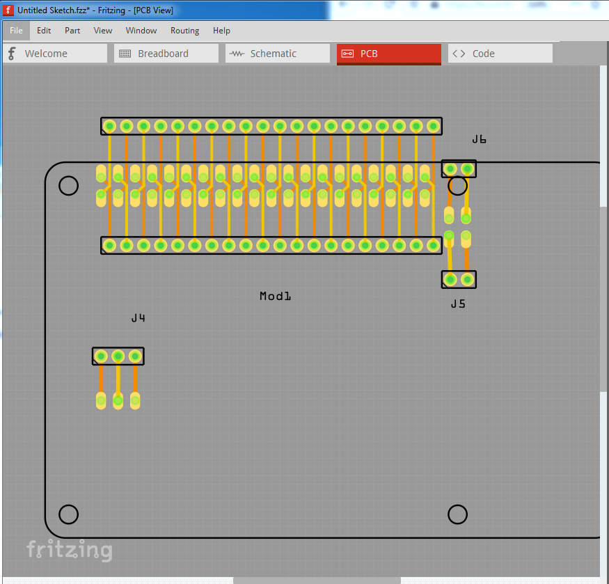
Although no one in their right mind would route this way other than as a test . I intend on changing parts factory to be able to emit this same pattern for headers and ICs, so look it over and see if you can see improvements. The test sketch this image is from:
rpi-4b-test-Sketch.fzz (68.8 KB)
and my version of the part (which will be in the temp parts bin of the sketch as well):
Raspberry-Pi-4B.fzpz (43.5 KB)
Peter
I just rearranged it… Yours is far better for pi 4…
I’m swapping with yours, just need to change the mini-HDMI ports, cause pi-4 has micro-HDMI, then it’ll be perfect (also usb-3 color)… ![]()
Yes, I missed that… ![]()
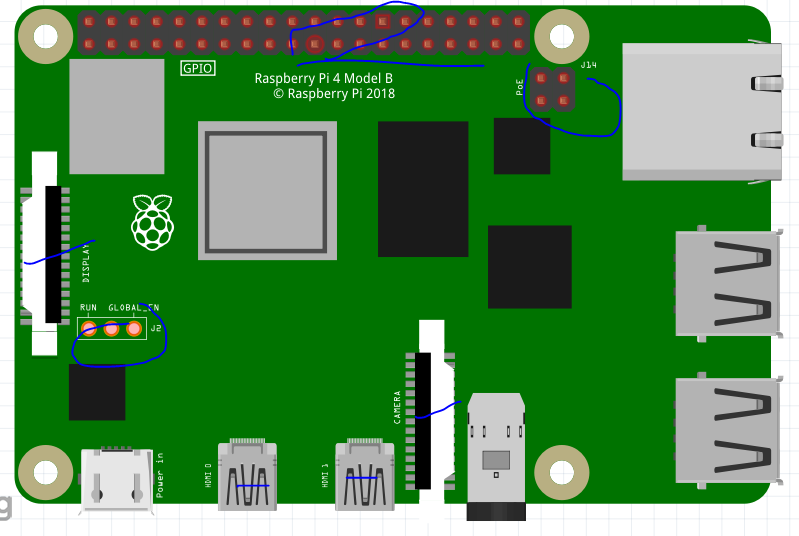
I think that’s for reset and AV output, as per as pi-zero… Old fritzing parts doesn’t have it, so I also leave it…
Sounds good, once we get a good one we can submit it to core parts.
Peter
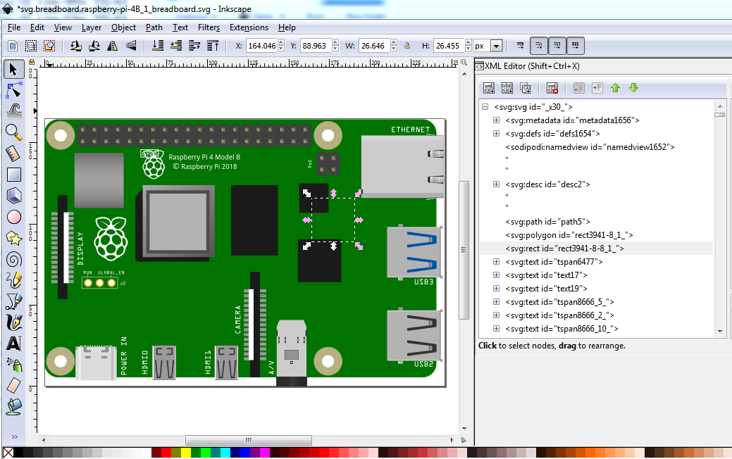
I’ve to fix all the pins on your breadboard…
You edited it on inkscape, so it took me a couple of hours… 
I also change some old design to match the new one… (all marked)
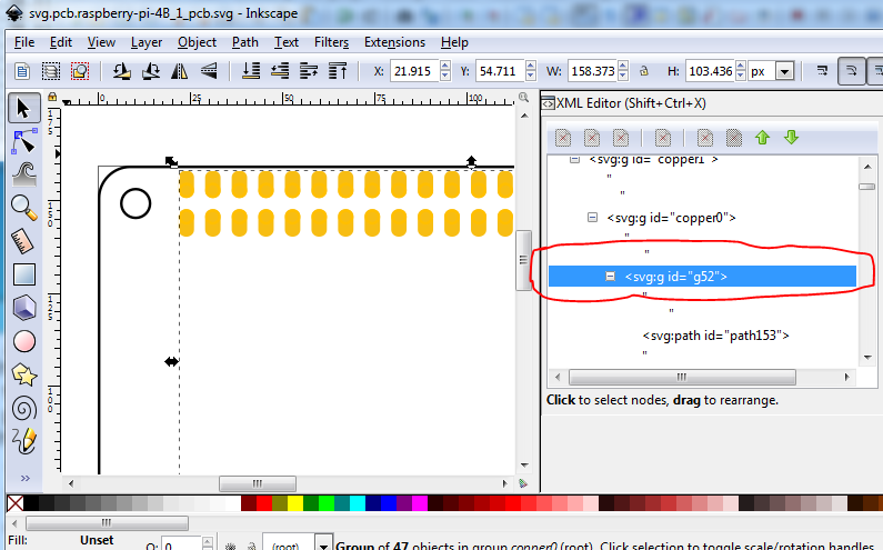
And, In pcb, I don’t understand why there is no hole on pins…? Is it ok?
Or you forgot to combine those paths…!!

Here is the edited file:
Raspberry-Pi-4B.fzpz (37.9 KB)
That may be my fault. Lxml is one of the few programs that obeys the space:preserve command and leaves the blanks in the xml. It annoys me when I’m editing so I delete the space:preserve (then lxml deletes the redundant spaces). I think Illustrator wants the space:preserve to work, so probably adding it back in at the top of the svg would have saved those hours of work. Sorry about that …
So far as I know you can’t make oblong pins as a single path. You can make a circle as a path, and gerber will drill a hole. Every thing I have tried with oblong paths with holes in them doesn’t drill the holes in gerber processing. In this case there are the paths (46 of them) then 46 circles (which are the connectors) which over lay the paths. As a bonus, changing the radius of the circle will change the hole size (at least in Inkscape) easily without having to recalculate the path to change the size of the circle. As I said this is the only oblong pad that I know of that works in Fritzing (at least and drills holes in gerber output.) I’ll look over your changes now.
edit:
Lots of problems!
Breadboard:
layerId should be breadboard (not breadboardbreadboard which is specific to breadboards and may trigger unexpected code)
It is desirable that all the connectors be at the very bottom of the svg in group schematic like this
(from the original extracted from vi)
    <circle
      cx="329.37469"
      cy="171.59525"
      id="connector0pin"
      r="29"
      fill="none"
      stroke-width="10"
    />
    <circle
      cx="329.37469"
      cy="71.609756"
      id="connector1pin"
      r="29"
      fill="none"
      stroke-width="10"
    />

 ...
    <circle
      r="30"
      cy="1430.1786"
      cx="428.83005"
      id="connector45pin"
      fill="#ffffff"
      stroke="#d4aa00"
      stroke-width="10.41666985"
    />
    <circle
      id="connector46pin"
      cx="528.82977"
      cy="1430.1786"
      r="30"
      fill="#ffffff"
      stroke="#d4aa00"
      stroke-width="10.41666985"
    />
  </g>
</svg>
The reason being that I have python scripts (as yet unpublished) that will number the connectors (when it finds the first item with an id of “connector”) in sequential order which reduces the work of defining connectors or renumbering them to add connectors in the middle. I would like to see all Fritzing svgs end up this way to allow tools to easily manipulate the svgs. For the same reason, I removed all instances like this

which is a stray unused connector which will confuse the scripts. This appears to be an invisible rectangle which could be removed.
This one I will remove becasue it shouldn’t be there (don’t know where it came from, it appeared when I ungrouped the svg.)

I have renamed all the connecotrxxpin_yy to polygon-123 and moved all the connectors to the bottom, then regrouped (but left the space:preserve)
<?xml version="1.0" encoding="UTF-8" standalone="no"?>
<svg
   xmlns:dc="http://purl.org/dc/elements/1.1/"
   xmlns:cc="http://creativecommons.org/ns#"
   xmlns:rdf="http://www.w3.org/1999/02/22-rdf-syntax-ns#"
   xmlns:svg="http://www.w3.org/2000/svg"
   xmlns="http://www.w3.org/2000/svg"
   xml:space="preserve"
   enable-background="new 0 0 245.968 164.34"
   viewBox="0 0 246.0628 164.24401"
where the xml:space=“preserve” is probably what Illustrator was unhappy about being deleted in the original svg. See of Illustrator likes this svg I guess.
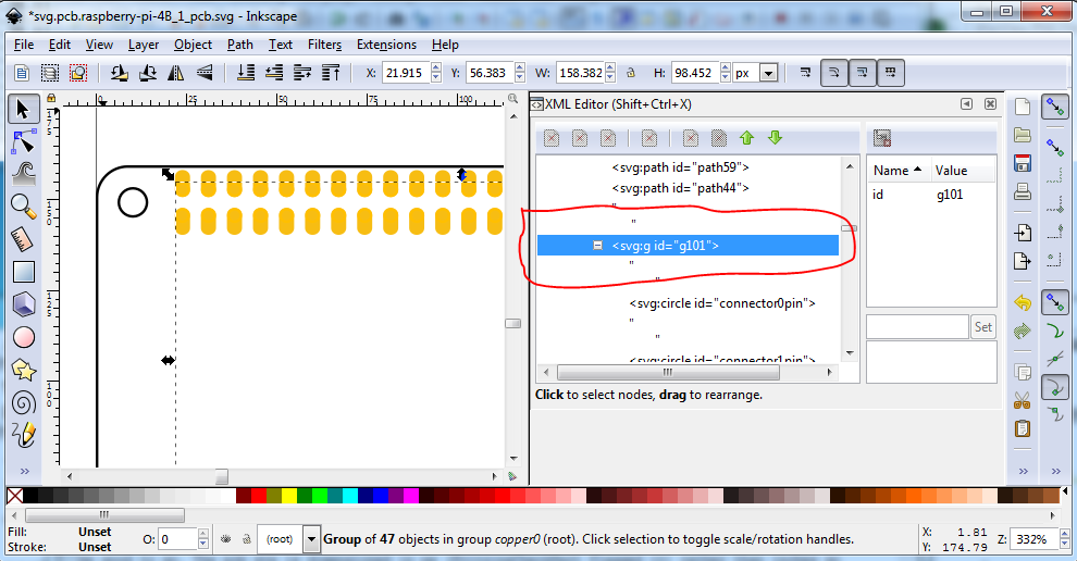
The fzp file still has the layerId as breadboard, so the breadboard svg layerId would have been wrong (FritzingCheckPart.py would have complained about it.) So see if this works in Illustrator and we should be good to go. The pcb svg is dimensioned in px (FritzingCheckPart flagged it) rather than inches so correct that. I see what you mean about no holes in pcb, something went wrong. That isn’t the pcb svg that is in the original file. It is missing all the connectors and is dimensioned in px. I’ll replace it withe the original correct pcb svg rather than try and fix it. Something (parts editor os a good candidate!) inserted some groups in to the copper0 group. This is part of the reason I don’t use parts editor it loves multilevel groups which screw things up!):
Ah! Something has replaced the fills in the connectors with fill:none again, this will likely work in gerber just fine (as it doesn’t care) but it won’t display correctly. The original svg has this
fill:#ffffff;stroke:#ffbf00;stroke-width:0.72000003
fill:none;stroke:#ffbf00;stroke-width:0.72000003
plus the scale is incorrect as well as being dimensioned in px (so perhaps this is an Illustrator issue). the original svg has an Inkscape doc properties that looks like this:
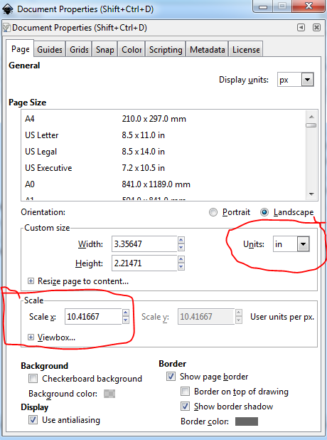
the svg in your fzpz has a document properties that looks like this (plus the extra groups and changed fill value):
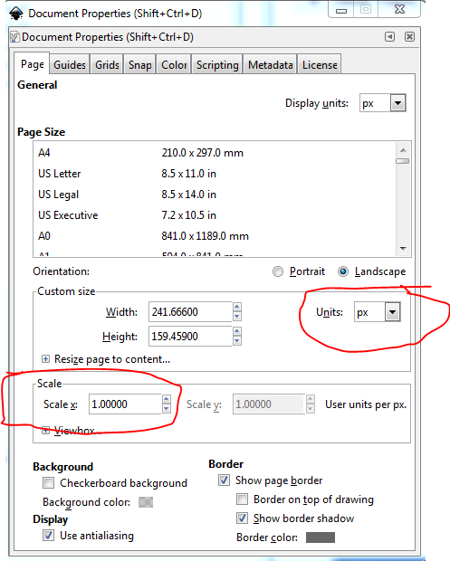
with dimensions in px (which can cause scaling problems) and the wrong scale. I’ll copy back in the original pcb svg. Just discovered the same thing happened to breadboard, it too is in px and at the wrong scale. It looks like Illustrator is changing the dimensions and scale when it edits Inkscape documents. We need to figure out how to stop it from doing that and get it to write the correct dimensions and scale because we eventually (when I finish an upgrade) want to put FritzingCheckPart.py in to the parts acceptance tool chain and it will insist on the correct scale and dimension settings. Plus I just found more problems. the scale in breadboard is indeed wrong, the pins are no longer on .1 boundaries:
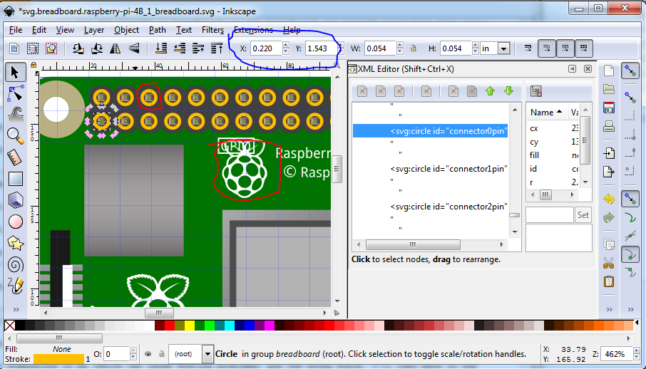
the copper circles were set invisible (fill:none and stroke:none) in the original and now have values again and the rpi logo circled in red should have been deleted. As well the xy coords of connector0 displayed here are no longer scaled on 0.1in boundaries when I display connecotor1 (presumably because of the dimension being in px with an unknown DPI setting.)
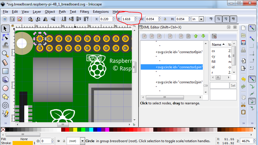
The y coords here should be 1.643in not 1.618in. It is getting late here, I’ll poke at this some more tomorrow and see what I can do. I can probably rescale this svg and remake the changes in the original in Inkscape, but I expect we need to figure out how to get Illustrator to not change the scale and set the dimensions to px to successfully interoperate with Inkscape.
Peter
1 Like
Oh, I don’t know how this happened…!!! Maybe, It was in the core svg, I didn’t rename any connector pin…!!
I don’t know how to fix it, Inkscape use px, but in AI, it use pt/px/in…
Suppose, any core svg, I open in AI, All the stroke are huge…
AI shows that, the stroke is 20pt/ 10pt/ 5pt… (actully mili inch)
I’ve to type them as .02in/ .01in/ .005in… And then It get proper stroke…
I think AI doesn’t support mili inch… Both editor save the svg as their own scale…
So, If a svg created on inkscape, I still can edit it in AI, But, created with AI, can’t edit in inkscape, the whole scale changed to px…!!!
I think we just haven’t found the correct settings for Illustrator yet. This used to work, as many of the parts in core were made with Illustrator, but I don’t know of anyone still posting in the forums that uses Illustrator. If someone reading does know Illustrator please post! Doing a google search for “illustrator scaling” brings up instructions on scaling a document (much like Inkscape’s) so I expect this is possible somehow, we just don’t know how. This page may be illuminating:
https://helpx.adobe.com/ca/illustrator/how-to/create-new-document.html
It appears to be similar to the Inkscape equivalent and I expect things like document scale and dimensions (inches rather than px) can possibly be set here, although I don’t have Illustrator to try it. I’ll rescale or copy/paste your changes in to my original file in Inkscape and see if I can pull your changes across in to mine.
Peter
Is there any problem with using Inkscape except to get scaling correct?
BTW i found this
https://wiki.inkscape.org/wiki/index.php/Units_In_Inkscape
EDIT:
I see version 1.0 is in rc, looking good https://wiki.inkscape.org/wiki/index.php/Release_notes/1.0 /EDIT
I am a newbie to SVG and Inkscape, just investigating yet…
Other than some annoying bugs (you can’t copy values via clipboard from one Inscape instance to another is an annoying one) Inkscape works fine. I use it exclusively to make parts. Having units in px is a problem, because a px has been 72DPI (early illustrator), 90DPI, (Inkscape prior to version 0.9.2 or 0.9.3) and now 96DPI. Fritzing will try and guess which one was in use with the svg but sometimes gets it wrong (in which case the part scale is wrong.) An inch is an inch at any dpi, so in or mm are the preferred dimensions, but figuring out how to set that in the various editors is a challenge. The last I tried the Inkscape V1 beta (which is probably 6 months ago) it had problems with rescaling that made it unusable. They may have been fixed by now, but I still use 0.9.4.
Peter
OK, I used copy and paste via Inkscape from your updated breadboard in to my original to move all your changes (I hope anyway!) across:
breadboard:
Move the GPIO and PoE connectors down to be centered with the mounting holes as they should be (and are in pcb).
Replace the display and camera connectors with your better versions and place them appropriately.
move the run global_en jumper block up to the same position it is in in pcb (overlayed the pcb svg to get the placement correct)
replaced the 2 HDMI Mini connectors with your HDMI micro connectors and added the larger HDMI label
Replaced both USB connectors with the ones from your svg and added the labels for both USB ports and the ethernet (which when I looked closely at my 4B I see are really there :-), good eyes!)
Increased the size of the Raspberry PI logo a bit to make it more accurate with the one on the board. So breadboard now looks like this:
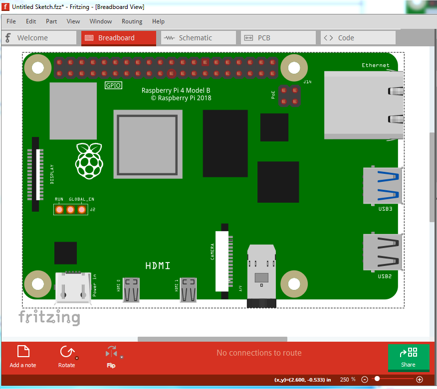
which came from this new part:
Raspberry-Pi-4B-2.fzpz (39.5 KB)
So please have a look over the new part and see if you see anything else I have missed. Schematic and pcb are the same as in the original part (I don’t think you made any changes in either of those, although Illustrator looks to have .)
Edit: just noticed the camera connector didn’t get updated correctly. I’ll fix that and replace this! It is obviously my day for weird problems, the svg is correct, Fritzing is just rendering it wrong for reasons as yet unknown:
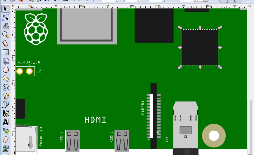
the white bar shows up much too large in Fritzing yet I can’t so far see a translate to explain that.
edit2:
Fixed. Replaced the path with a rectangle and now it renders correctly. Don’t know why that one path doesn’t render correctly though:
Raspberry-Pi-4B-3.fzpz (40.0 KB)
Peter
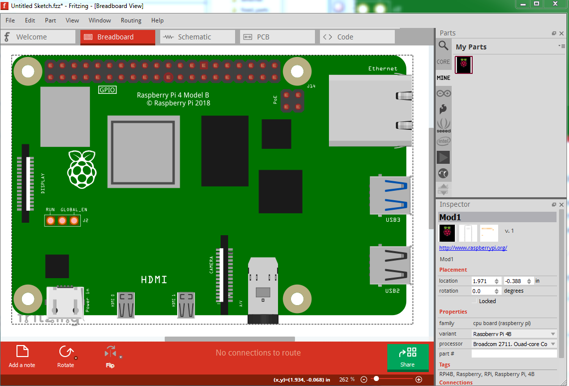
It’s ok, But PoE pins, Run & global pins aren’t at right place…
And due to inkscape scale, micro-Hdmi & USB (from mine) svg get smaller…!!
I’ll check them again against the mechanical drawing (and print out the footprint since I have a device to compare it against this time!)
That is why dimension in in or mm is a better bet. Illustrator must be using a different DPI value (perhaps 90DPI instead of 96DPI) than Inkscape. I’ll see if I can figure out how to scale it. Thanks!
Peter