Good day, Peter, I need your support again.
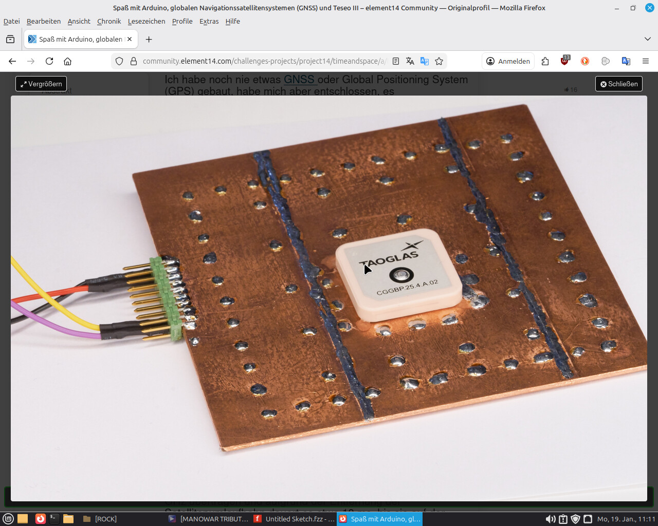
I built a GPS watch, and its reception is poor.
I need a larger ground plane = a double-sided PCB that I can drill through and pass wire through, then solder it.
I need a 24.3X24.3 opening in my board—how do you achieve this?
This would be the PCB (still have to think about the size-…either 80X80 or 70X70 mm).
Could you please lend me a hand with that?
Thank you in advance
Regards
Hans Werner
The part should look similar (more professional), industrial quality!
Asia? It’s big! I know from Peter that he comes from Canada
PS… the PCB with the square (4eck)—could it perhaps be designed so that its size could also be changed if needed?
I don’t know the size; I only received a recommendation…
either 60x60 / 70x70 / 80x80 mm…?
Ok for this you can try overlaying multiple holes to form a big square hole (someone tried this before but can’t guarantee that to work. Try searching the forum.
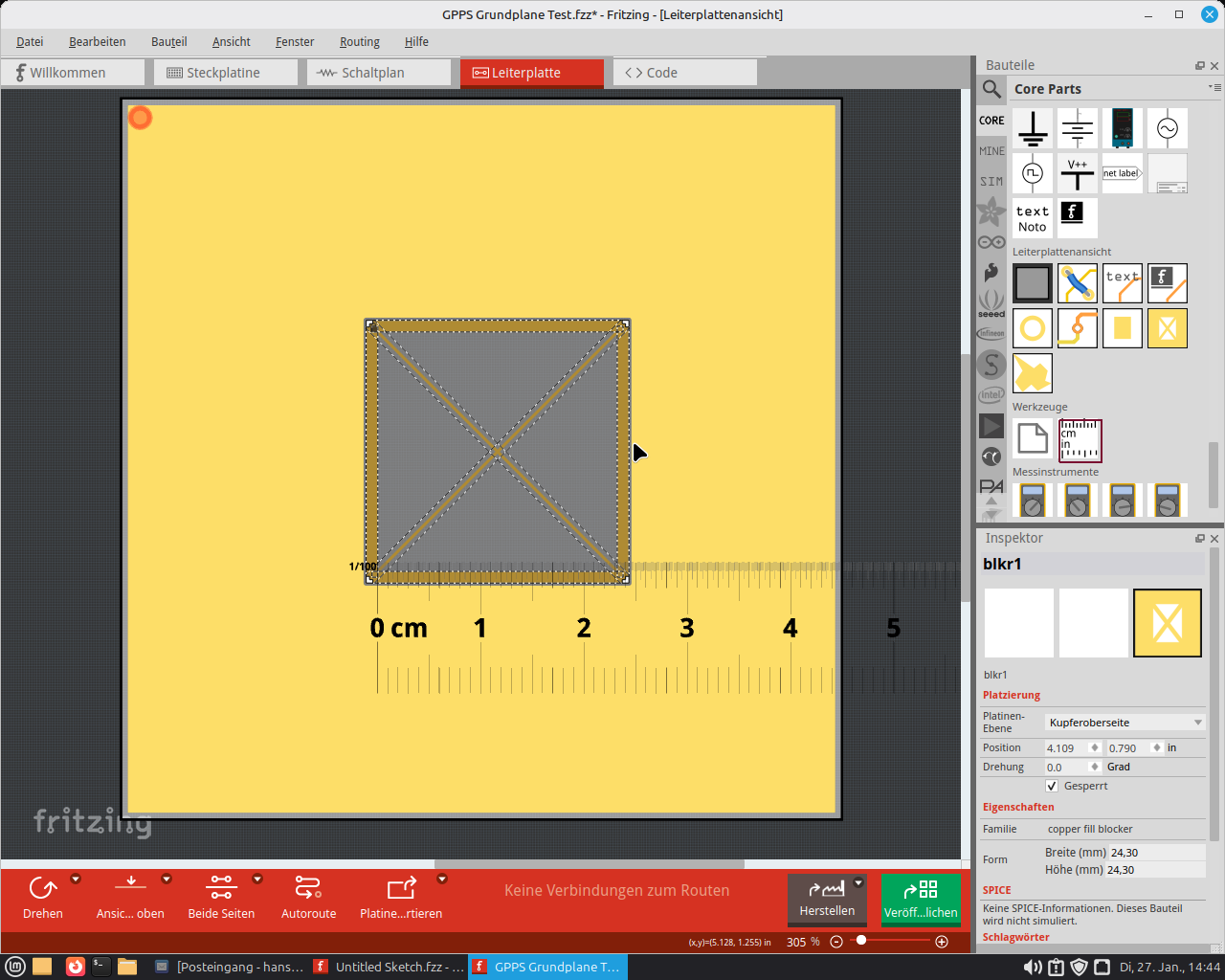
Wie about the copper fill keepout (Copper fill Stoper)? That creates an area without copper, right? Then I’d have an area without copper—could I cut that out?
So, I took a look at it…
I created a double-sided PCB with a copper pour keepout (Füllstop).
The spacing on the inside has the desired 24.3 X 24.3 mm; on the outside it is larger—can the larger outer ring be used as a solder pad?
Then is it best to use phenolic paper (Hartpapier) and maybe saw it out by hand yourself?
A cutout tool for Fritzing (to draw rectangular or other cutout shapes) is still on our wishlist.
Until then, you can draw the shape in an SVG, use the oposite orentation for the cutout.
Like so:
<svg xmlns="http://www.w3.org/2000/svg" viewBox="0 0 70 70" width="70mm" height="70mm">
  <path d="M 0,0 L 70,0 L 70,70 L 0,70 Z M 22.85,22.85 L 22.85,47.15 L 47.15,47.15 L 47.15,22.85 Z"
        fill="currentColor"
        fill-rule="evenodd"/>
</svg>
The complete SVG then looks like this (with silkscreen outline):
<svg xmlns="http://www.w3.org/2000/svg" viewBox="0 0 70 70" width="70mm" height="70mm">

<g id="board">

  <path id="boardoutline" d="M 0,0 L 70,0 L 70,70 L 0,70 Z M 22.85,22.85 L 22.85,47.15 L 47.15,47.15 L 47.15,22.85 Z"
      fill="#ffffff"
      fill-opacity="0.5"
      fill-rule="evenodd"/>

 <rect id="silkscreen" x="0" y="0" width="70" height="70"
        fill="none" stroke="white" stroke-width="0.2"/>

  <rect id="silkscreen0" x="0" y="0" width="70" height="70"
        fill="none" stroke="white" stroke-width="0.2"/>
</g>
</svg>
If you save this into an .svg file, you should be able to use it as a board in Fritzing,
see “load image file” for the PCB in the Inspector
SUPER! AWESOME!!! but I only have program code… the SVG is missing.
What I still miss in Fritzing is when I optimize components in the schematic…
e.g., resize a resistor, adjust display settings for what Fritzing should show, etc…
when I then go to the PCB view I have to set everything up again, that’s annoying and slows me down… actually just minor details, but really helpful.

