Good day, I need help with the design of the connector (this is a pcb card so only pinout for golden fingers) and the pcb board shape for my new project. (Internal IO card for PC) I make some parts for my, but this application is extremely difficult for precision. So I will be happy if someone with more experience can help me with these files. I found the PCIe connector manual and drawing for this card. (I need a card 35x95mm). Thank you for your help.
It is unclear to me what you need. The pdf is a connector intended to take a board. I assume your pc already has this connector and you are looking to make a board with a gold plated edge connector (rather than a Fritzing part for the connector?) If so the footprint for the connector isn’t likely useful, we would need the specifications for the fingers on the board (which are likely to be slightly different than the connector footprint. As well we would need to know where the fingers need to be in relation to the edge of the pcb. This site
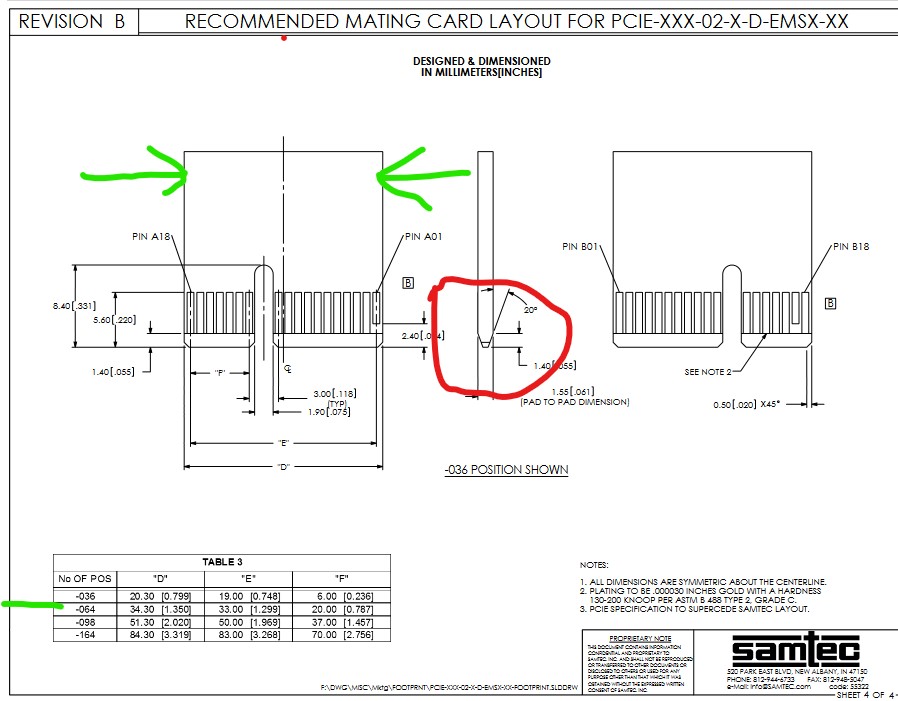
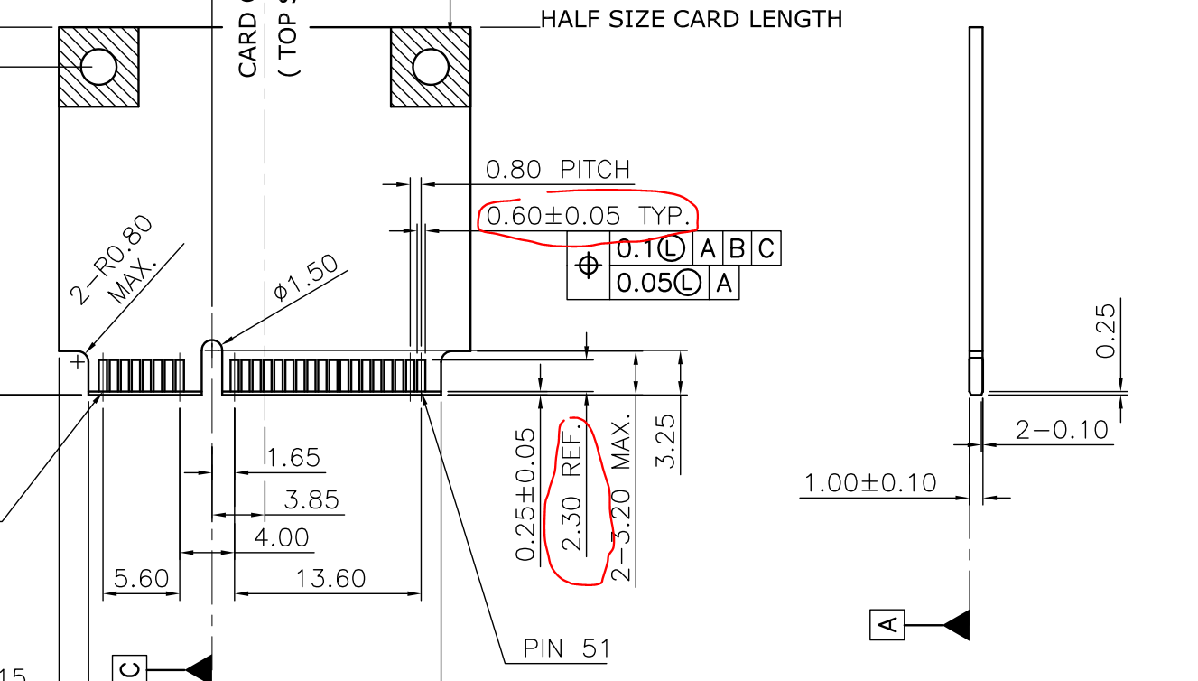
has part of the layout of the pcb side of this (the width of the fingers is not specified and will need to be found from somewhere.) There are a few issues though. The slant on the bottom of the edge connector can’t be specified in Fritzing (the red circle), the number and pitch of the pins needs to be found somewhere as well.
Peter
Hello, yes I need the pcb side. But I sent a datasheet of this connector, because there is a layout of the opposite side (PCB). on page 9
I think that there is all the information about it. And this red marked angle shouldn’t be a problem if I send email to the company which will be making these pcb. Thank you again.
Ah! I saw the package and pick and place drawings and stopped reading in the pdf. Indeed the needed information is there. I see that all the pins in the pdf are the same length, in the other image notice that the end pin is shorter (likely the power pin to allow hot swapping which you may not need but it would be best to check!) That may cause a problem if they need the pins to all be shorted together for plating though. I haven’t done a gold plated edge connector board in 40 years or more, so the other thing to check with the board house is if they still need all the pins on the edge connectors shorted together by a trace that will be truncated like this
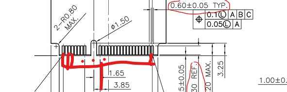
the red lines on the bottom connect to each pin so the pins all connect together to allow gold plating via electoplating. After that the board is truncated to the bottom of the edge connector to isolate the now plated pins. It would be wise to check if this is still expected / needed these days. It is possible they can just dip the pins in a solution and plate them these days and no longer need the short. As well edge connectors in Fritzing are a special odd case that requires separate copper1 and copper0 layers (which is supported by Fritzing but not by parts editor) so you need to be comfortable with directly editing the svg and fzp file to make this board Parts editor won’t work for it. This tutorial set may have the edge connector layout in it (I don’t remember at this point) but is in any case what you need to be comfortable doing to make this board.
looks like edge connectors are here instead
Peter
Good morning, the pins don’t have to be shorted. And the length of the pins is the same. Hot swap will be supported, but with a microcontroller. So it doesn’t matter on the length of the pins. These two holes on the top are not necessary for me.
OK this should do what you want (and as a bonus it will work with parts editor!) It comes as a 3 part make a connector kit.
svg.pcb.119A-40A00-R04-board_outline_1_pcb.svg
(right click on the image and “save image as” to recover the svg)

and two Fritzing SMDparts
119A-40A00-R04-pcb-con-bottom.fzpz (9.6 KB)
119A-40A00-R04-pcb-con-top.fzpz (9.5 KB)
then there is some assembly required ![]()
First start Fritzing and go to pcb view and select the default grey pcb, then click on load image file in Inspector
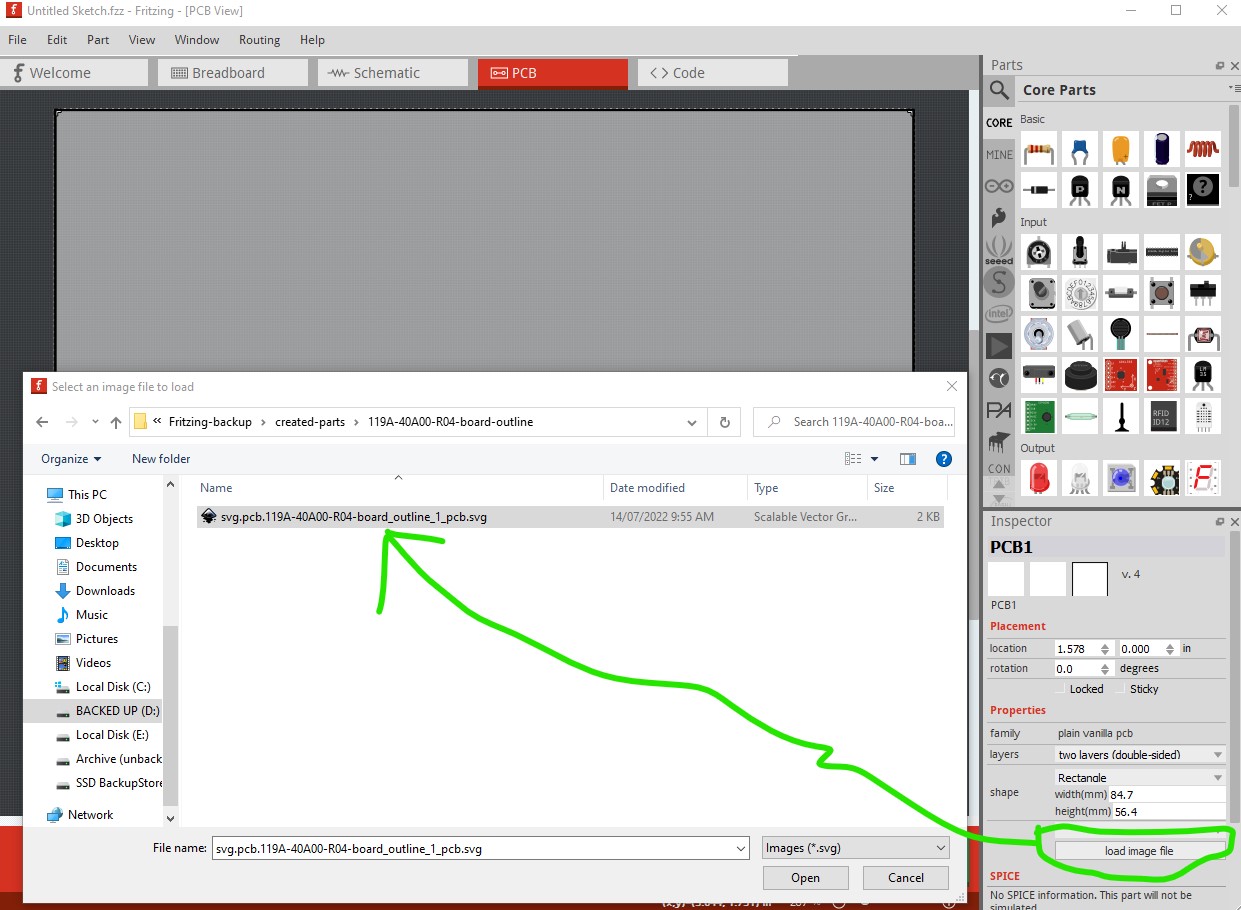
navigate to the board outline svg and load it. You should get this
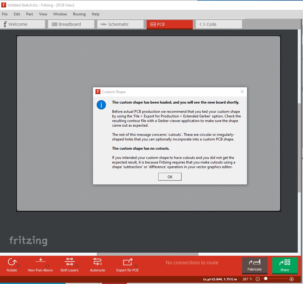
click OK and you should get this
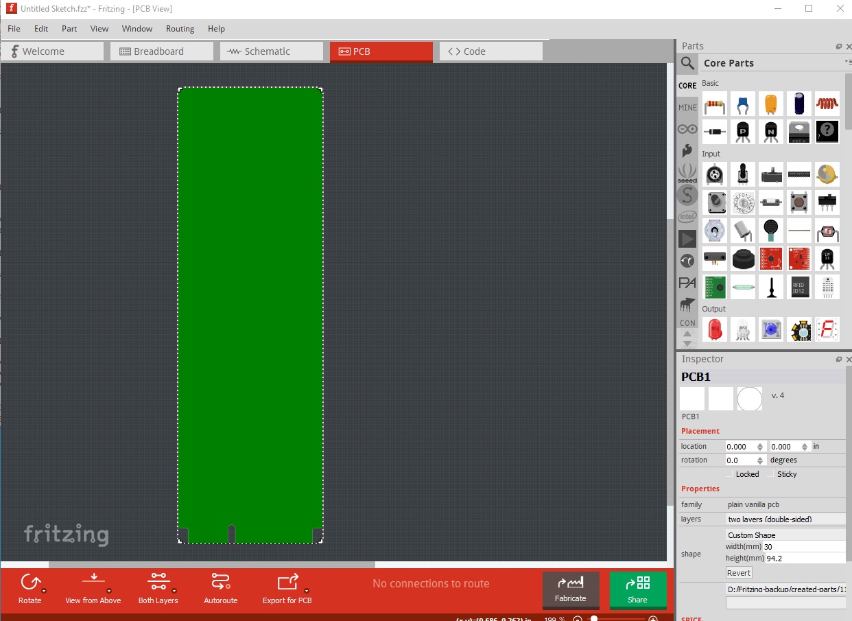
which is the outline of your board (non standard 95mm tall!) Now you need to load the 2 fritzing connector parts and place them on the board (which is a little tricky!) Let start with the bottom connector (as it is a bit odd!) So select the 119A-40A00-R04-pcb-con-bottom part and drag it in to the sketch. Note it appears to be the wrong way (because it is on the top of the board instead of the bottom) so click on the board layer in Inspector and change it to bottom to put this part on the bottom of the board. I also hid the label as it isn’t useful. That should result in this:
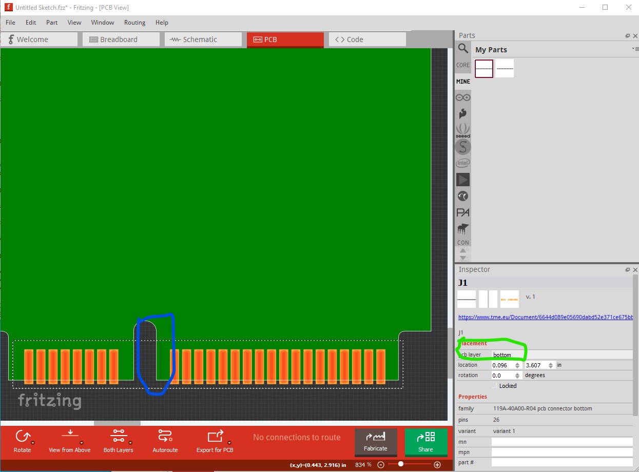
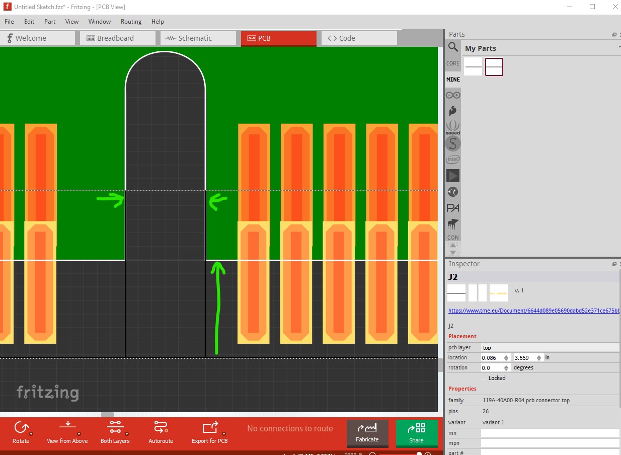
Here the blue circle is around a 1/1000inch line on silkscreen that is used to align the connector to the bottom of the board and the center slot like this:
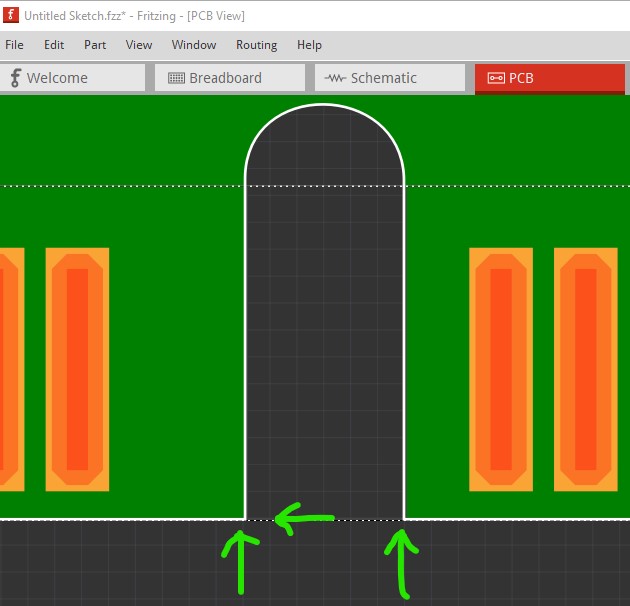
here the two vertical lines are overlaid by the white silkscreen of the slot, and the bottom of the part is on the bottom of the board to give the desired 0.25mm of space from the pins to the bottom of the board (the dotted white border of part should align with the bottom of the board!) Now do the same (except don’t move it to the bottom layer!) for the top connector part and you should be away.
The two parts pin labels match the pin numbers on the connector. It would be wise to lock both parts once they are aligned so they don’t get accidentally moved! The top part makes the alignment lines much clearer!
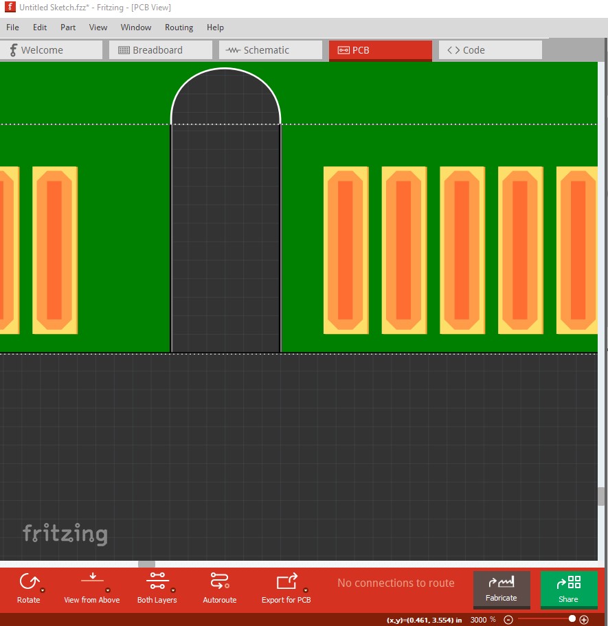
and shows the pins line up (at least when moved up so the bottom of the board is correct!)
the contour.gm1 gerber file (displayed in gerbv) shows the correct board outline
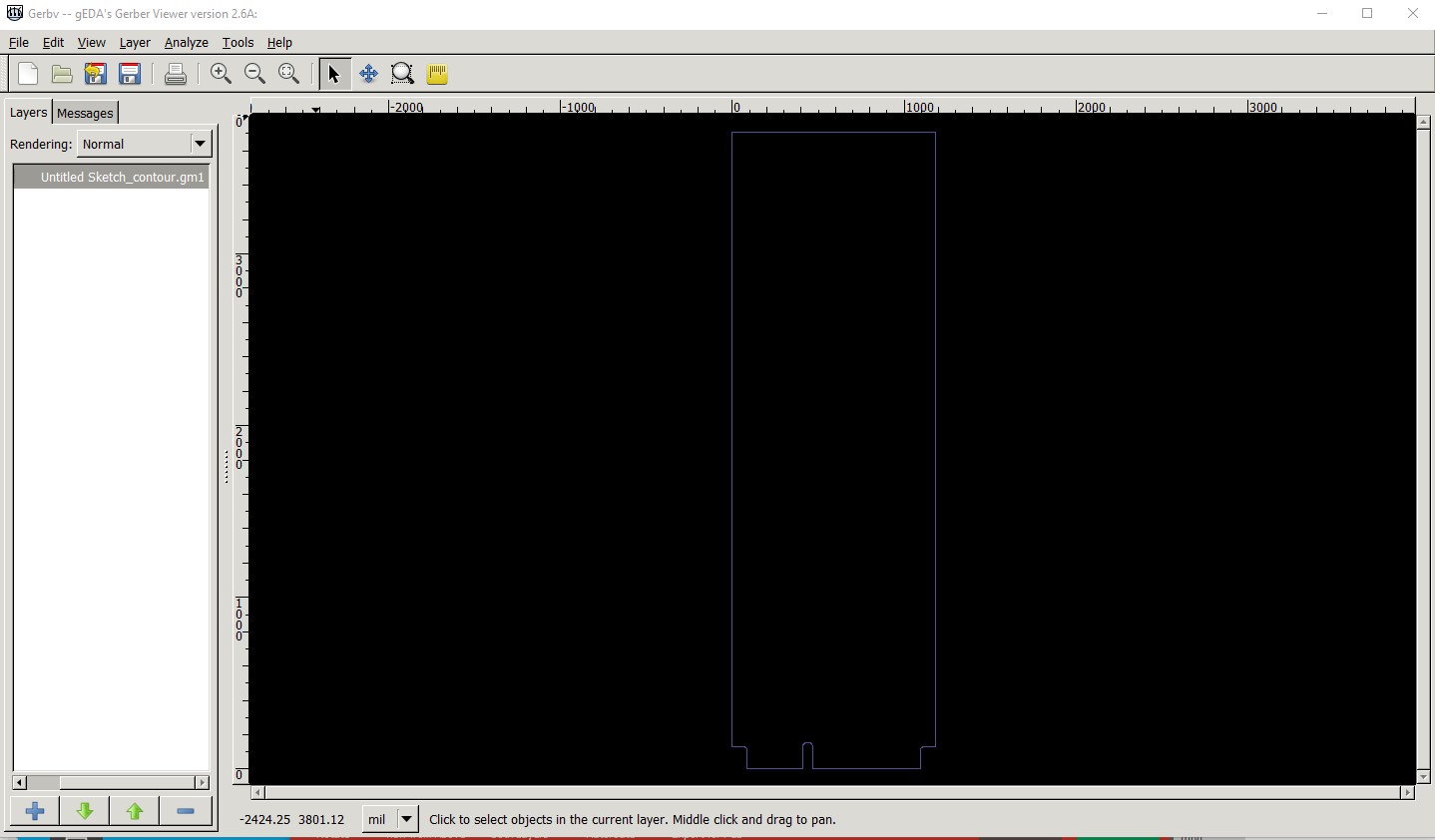
but the silkscreen doesn’t look to have rendered quite correctly, but it also doesn’t matter as the contour.gm file will cut the board correctly.

Here is a copy of the sketch that the gerber output came from as an example.
connector-installed.fzz (20.8 KB)
Peter