Hi Guys.
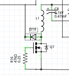
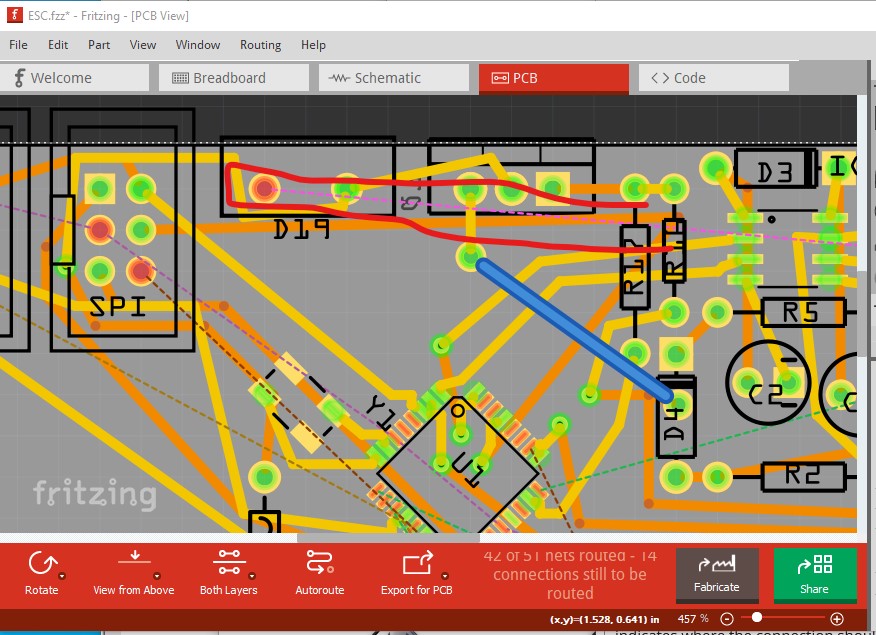
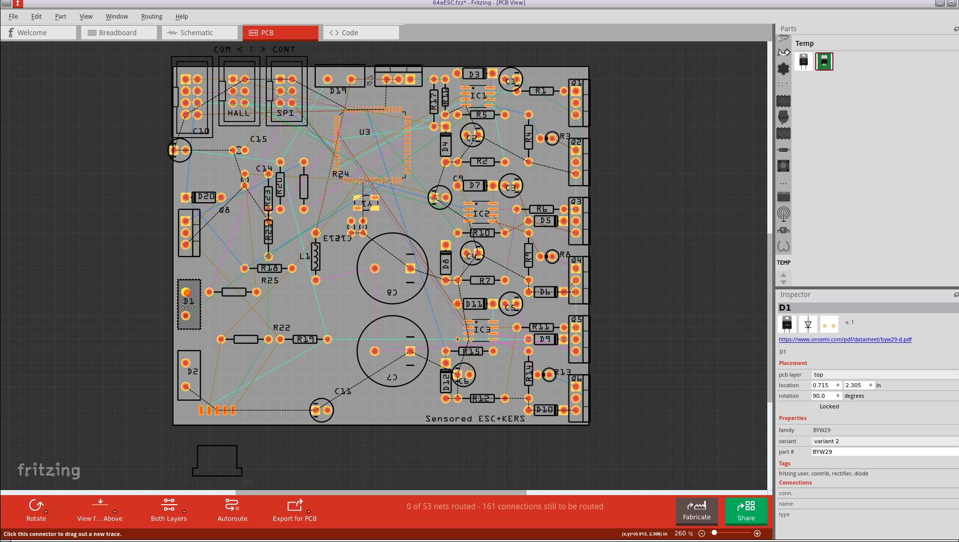
I have a diode that in the the schematic shows both anode and cathode connected to other stuff (if I click on the connections I can see the yellow dots lighting up where is is supposed to be connected to) , but in the PCB the cathode is connected to nothing even after save and autoroute.
What is causing this and how do I fix it without manually creating the track in the pcb ?
Please upload the sketch (the .fzz file, upload is 7th icon from the left in the reply menu) it isn’t possible to see what is wrong from the images. That said if you click on the various pins (such as the drain of Q7 and inductor L1) all pins that are connected should light up yellow like this:
Anyway here’s the sketch attached. (ignore the breadboard view … never even bothered with that) ESC.fzz (50.6 KB)
Basically I’m taking to pcb something I have already working on perfboard:
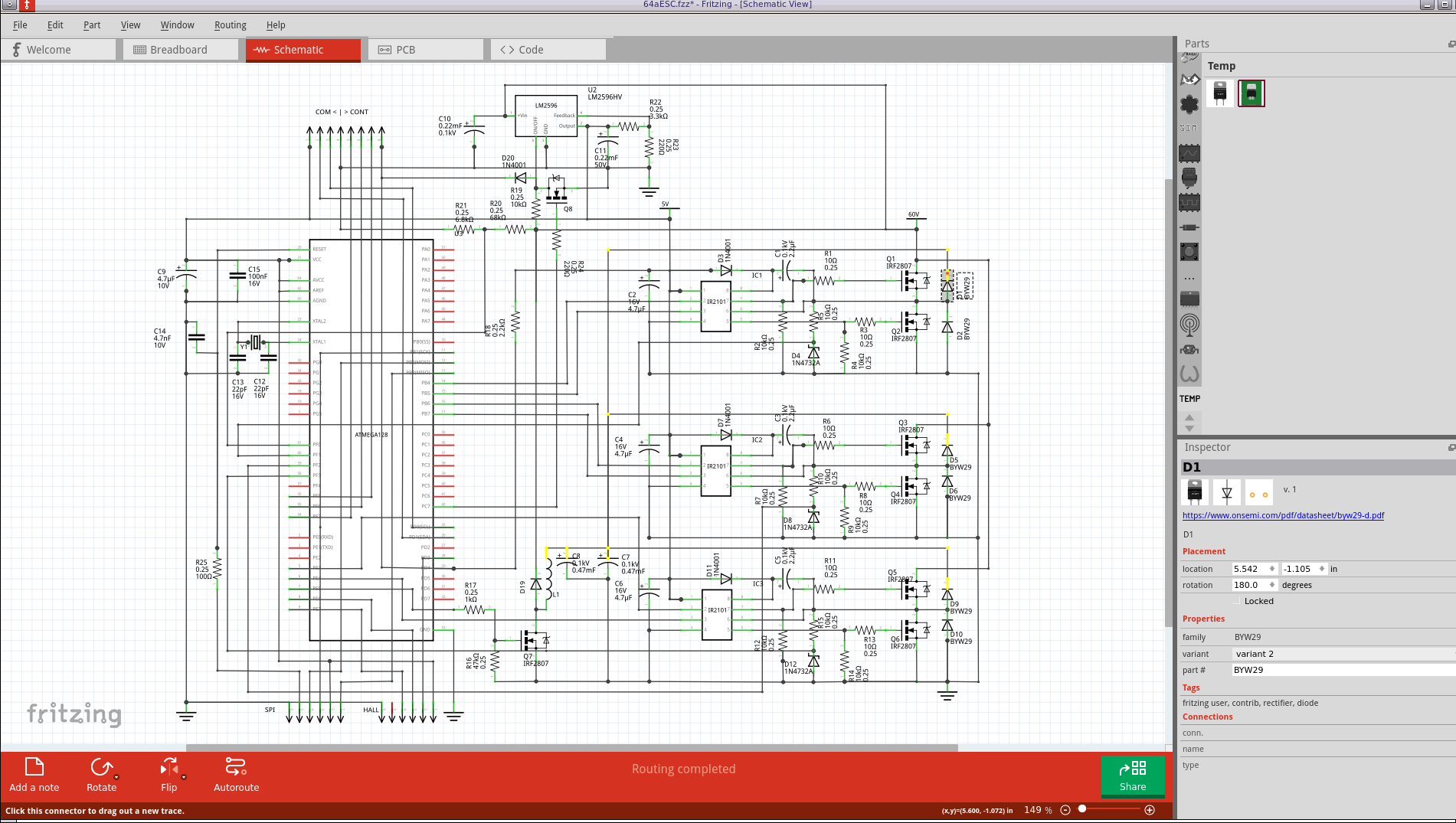
It is a ESC for Sensored Brushless Motor (DIY e-scooter project).
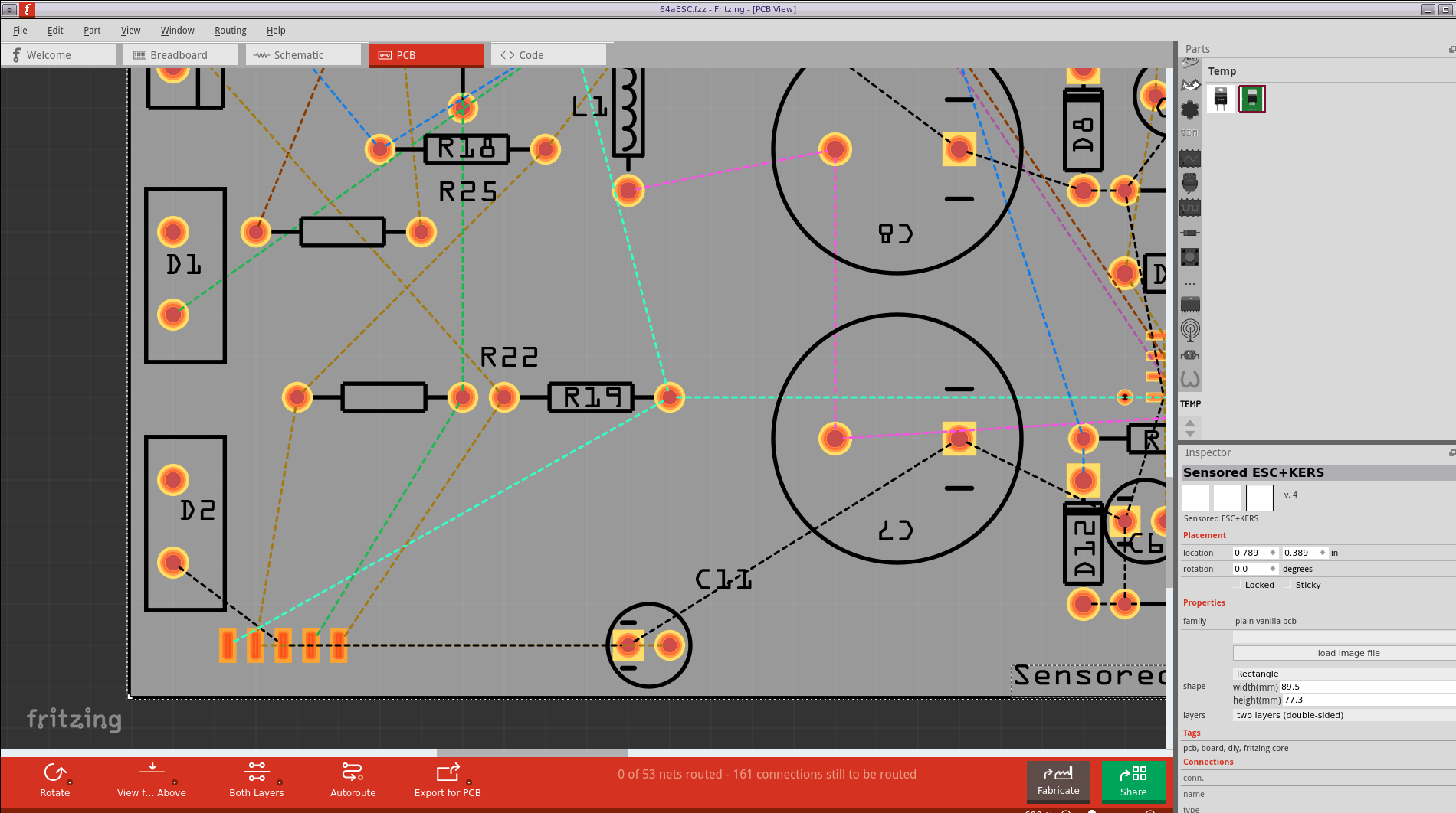
I did a cleanup and removed all the unnecessary bend points.
Autoroute still fails to route some traces … maybe I should relocate some components to make it easier for Autoroute ?
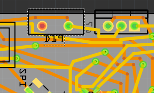
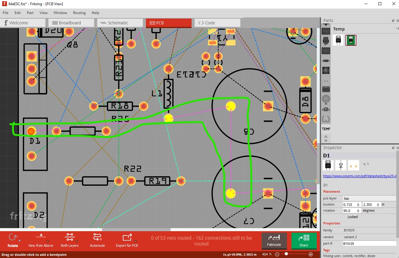
Sorry, missed that. That said I think this is an image problem. The image above I think may have a rats nest line, but it is to faint to see in the image. When I autoroute your sketch it ends before finishing but the diode has a rats nest line that indicates where the connection should be as expected:
Note the pink rats nest line from the diode (circled in red) which indicates a not yet routed connection.
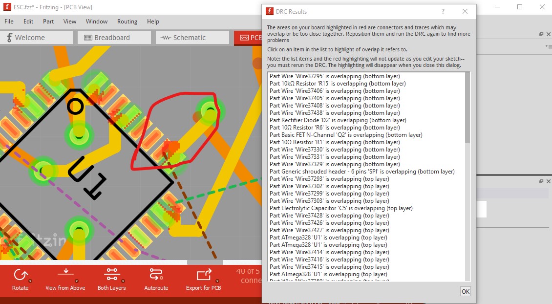
That is one solution. Another is upping the allowed autoroute cycles (which costs time) here I used 1000 (up from 100.) The result however isn’t any better. In general autoroute is a bad idea as it isn’t very good. You are far better off to hand route the traces based on the rats nest lines. In addition there is a problem in the clearances and you will find that DRC reports a lot of errors of traces too close like this:
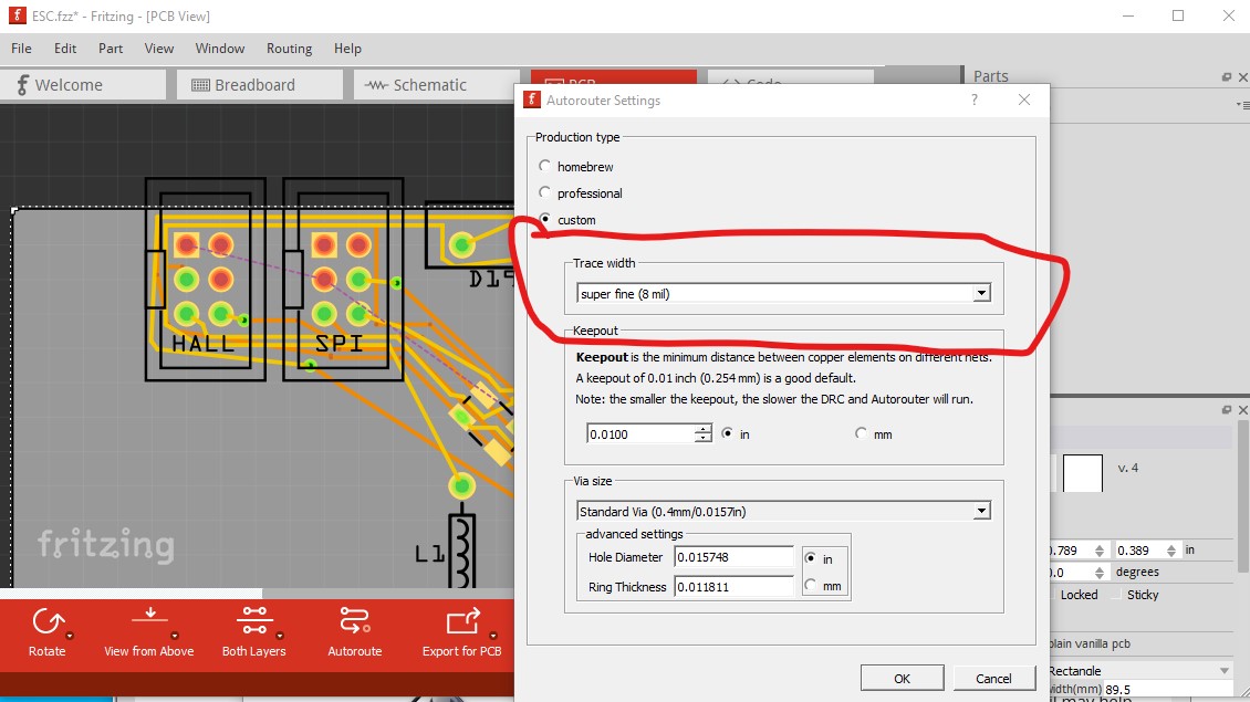
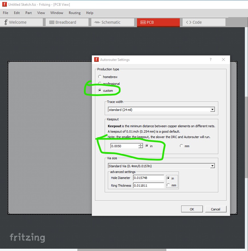
this is partly because the default trace size of 24 mils is too large for the SMD pads. Using the custom DRC/auto route settings to reduce the default trace size to 8 mil may help.
Hi Peter.
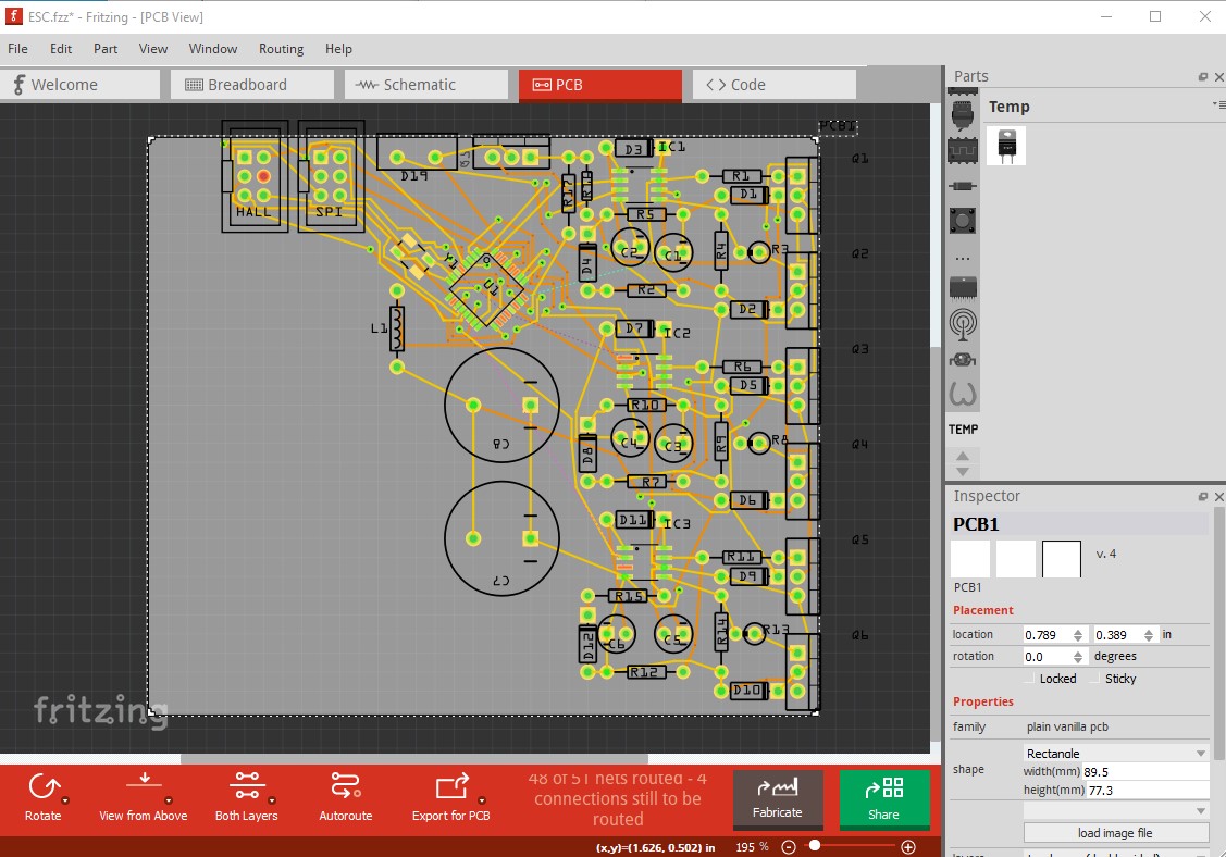
Thanks so much again for your help. If you still have the hand routed one would you share it ?
Thanks for explaining to me how the autorouting process ends up leaving a certain amount of traces as rats nests.
I’m totally new to PC assist in pcb fabrication … what are DRC errors ?
Where do I set the allowed autoroute cycles ?
I had already seen that for the power bridges and the KERS I would need to force thickest tracks … was not expecting to have to force thin tracks … again I’ve a lot lo learn ahead of me.
There is one more question that pops into my mind: if autorouting is already troublesome with such few components how on earth are computer motherboards routed ?
DRC : Design Rules Check - in Fritzing’s case, checking if all of the connection pads and traces maintain minimum distance from each other and from the edges of the board (or holes in the board). That distance is configurable, and the “required” value depends on the manufacturing process (tolerance) for the board (as well as electrical characteristics for some circuits).
Computer mother boards are designed with much more powerful layout programs, and they are also more than 2 layers (Fritzing’s limit). More layers means more possible paths to get the connections where they need to go.
I didn’t finish the hand route, just did enough to see that it is probably possible (a lot better than the autorouter!) You do need to set DRC down to 0.05in as the 328 part has fine pitch pads and fails DRC with the default settings.
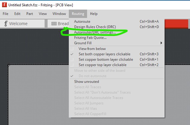
click on Router->Auto routing/DRC settings and select custom and set keepout from 0.01in to 0.005in like this.
either type a new number or use the increment/decrement bars on the right side to increase or decrease the number of loops.
Again the 328 part is small pads and the default 24mil trace is too large for it. As well larger traces take up more board area and make routing more difficult (both manually and for the autorouter!)
I haven’t used the really high end software (Pro engineer at +$100,000 per seat is one!) but I understand autorouting (which is a hard problem!) doesn’t work all that well there either. They may let autoroute do some of the work but I expect they finish it off manually. Human eyes are much better at seeing possible routes than any software I know of.
edit:
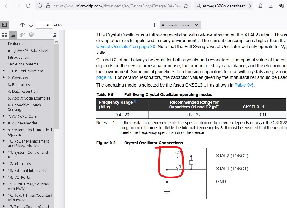
A few additional notes, you look to be missing some things. There are usually two capacitors on the crystal (from the 328 data sheet):
which are not present. There are also usually power bypass capacitors close to the VCC and ground pins on the micro, typically a 0.1uf ceramic cap for hs noise and a tantalum electrolytic for current surges although they appear to be recommending 10nf ceramic bypass caps. You likely also need both a reset and programming circuit (the spi may be the programming interface though) and I don’t see either of those. This paper
may be helpful about what is needed, as it covers all these issues. See the drawings on page 7 for reset and page20 and 21 for pcb layout examples for power decoupling and crystal layout.
I know, it’s not finished yet, but thanks for reminding me. I would actually like to use a much smaller xtal salvaged from a arduino nano clone I physically busted both MCU and ch340.
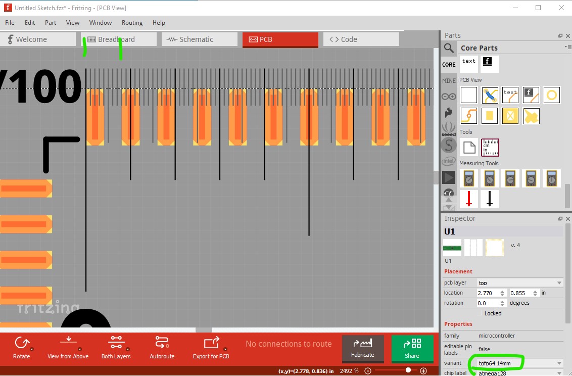
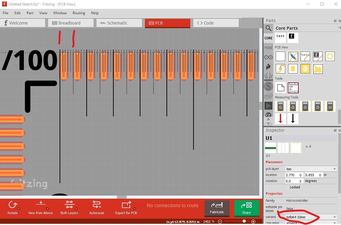
I have a more pressing issue: I ran out of IO pins on the atmega328p … I will have to rewire for atmega64a (of which I have 3 samples).
I guess I have a lot more work ahead of me for this project.
Assuming you mean a atmega640, there is at least a chip for it in the library I think. It will likely have a similar app note on the Microchip site for what it wants in bypassing and layout.
I once saw a youtube video of an expensive piece of software’s auto routing getting trashed by an engineer. I’ve never used auto routing as it doesn’t seem to follow good design practices.
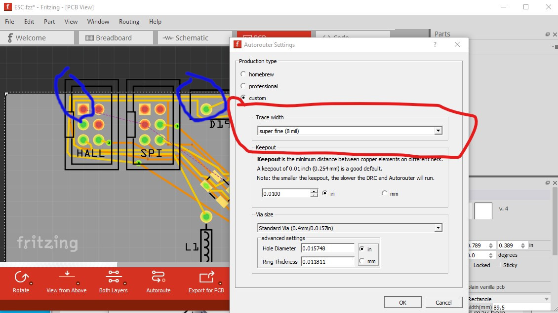
By this, I mean, as I know it, a square angle in a PCB trace is frowned upon…
The areas circled in blue are 90 degree angles, two 45 degree angles instead of one 90 degree joint is considered good design practices. It reduces noise and interference, I guess. But what do I know, I’m just a hobbyist…
You have lots of room on the pcb board that is empty, moving some components around might help the routing process. I would position the large capacitors close to the component they are connected to, and use thicker traces for them…
No I mean ATmega64A … it should be pin compatible with atmega128 and they both can come in tqfp64 package so I will use the latter to the schematic and pcb.
I plan to have some components on the under side flat so that they can dissipate trough the case …
Also the rectifying bridges to the motor wingdings used for the switching KERS will make the layout difficult … but maybe if I make the driver bridges vertical and the rectifier diodes for the rectifier bridges flat on the bottom side they can all fit like you suggested … I will give it a go.
Thanks for the suggestion Randy.
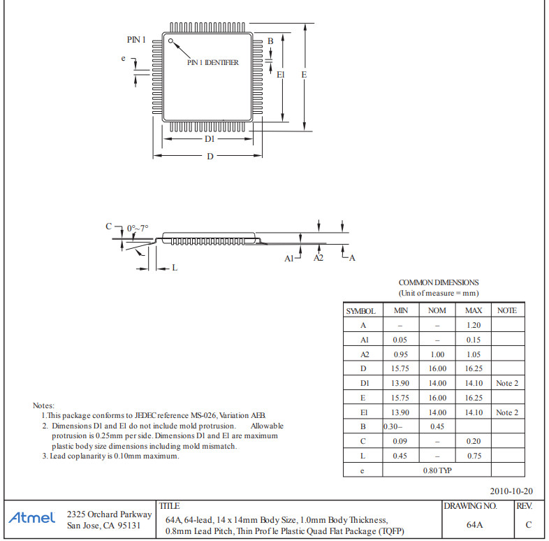
if 14mm means the leangth of each side of the square chit then I am ok … if not then how do I figure out ?
I guess I can use the grid which looks like standard dip spacing (1/10" or 2.54 mm) if that is the case the contacts should be around 5 and 1/2 grids.
I have an adapter which fits perfectly the chip… it is labeled TQFP64 0.8mm (which in this case means pin spacing) would that confirm it is a tqfn64 14mm ?
Actually the packaging section of the datasheet answers it
I know the layout is crazy at the moment … first I need to swap out the classical diodes D1,D2,D5,D6,D9,D10 with the vertical BYW29 … I just started doing that and I ran into this problem.
it has a rats nest line to the other connections. When I look closely enough at the image above the rats nest lines appear to be in it (if not very visible!) so I don’t know why the connections didn’t light up.