That is odd! I don’t have 0.9.9 on Linux at the moment so I can’t try Linux. Perhaps someone else with 0.9.9 on Linux would download your .fzz file and see if the D1 cathode rats nest lines appear for them. I seems odd that there would be a difference on Linux to me, but I guess it is possible. Doy you have Windows machine that you could load 0.9.9 on and see if it works for you there? I’ll try and put 0.9.9 on my Ubuntu installation and try it there.
Maybe … but where do I get a free 0.9.9. for windows ?
On Linux I initially built it from github … only to later find out that rpmforge has it already packaged.
I installed 0.9.9 on Ubuntu and you are correct it is a Linux problem. On Ubuntu D1 (looks like all the diodes in fact) are not connected to the capacitor even though they are in schematic. I’ll report it as a bug on github (assuming I can figure out how to get a screen shot on Ubuntu!) The Windows version of Fritzing is available from the Fritzing site, but may requires a donation for the download. Building on Windows is not simple.
edit:
Spoke too soon. When I tried again on Win10, it now fails there too so it isn’t a Linux problem but a bug of another kind that may be intermittent. This is a screen shot from Win10 just now with the same .fzz file from the one above, this time it looks the same as yours so there is something else wrong. I’ll poke at it more tomorrow and see if I can figure out what is going wrong.
Another bug to be aware of: complete schematic without making any traces in pcb or breadboard. There is a bug that we can’t reproduce where making a change in another view sometimes corrupts the routing database. If the database gets corrupted you can sometimes recover by deleting all traces in all views, but sometimes you have to scrap the entire sketch and start again.
But scrapping something with a couple of IC is one thing … scrapping something with 7 fets, 4 IC, 50 odd passive components and a 64 pin MCU along with 20 pins for external connector is another story.
I really hope I won’t need to start over again.
Well ubuntu is not my favorite Linux distro but there are a few hints I can give you that might work:
shutter is an app that takes screenshot of the desktop, or even the active window if you want,
gnome-screenshhot does the same thing,
xv also on older non wayland compositors.
Hope this allows you to take screenshot on your ubuntu.
I use a fairly original setup with fedora but I use a really simple window manager (fluxbox)
In my case I actually mapped the “Print SCR” key to activate shutter and grab the active window (allowing me to capture the yellow highlight).
Here’s the last line in ~/.fluxbox/keys file where I did that:
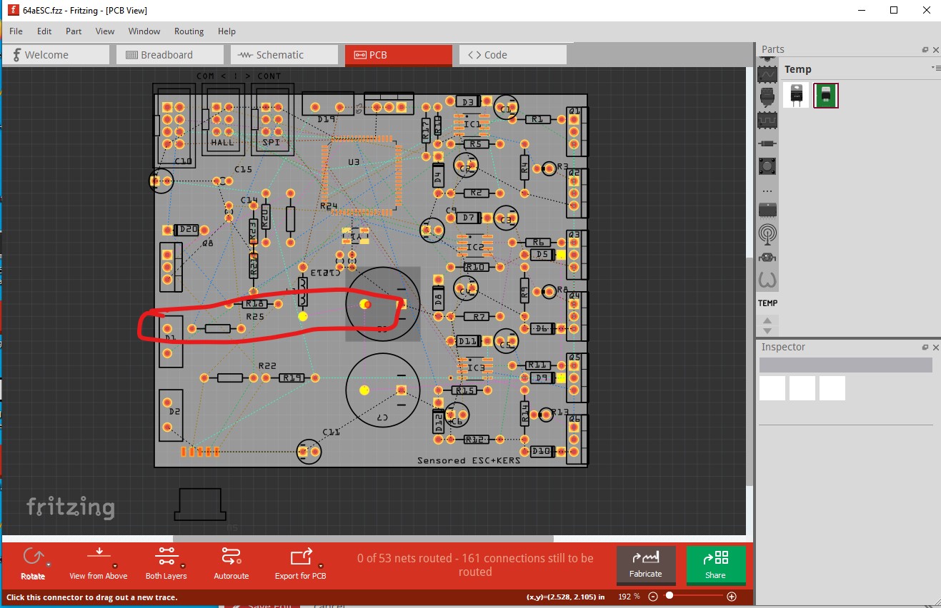
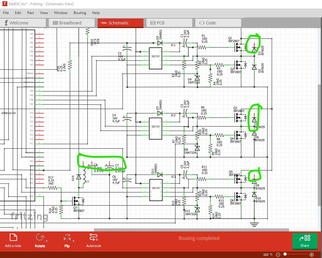
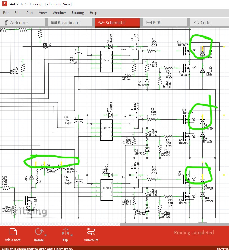
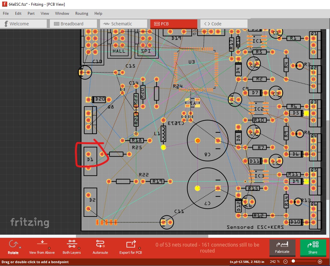
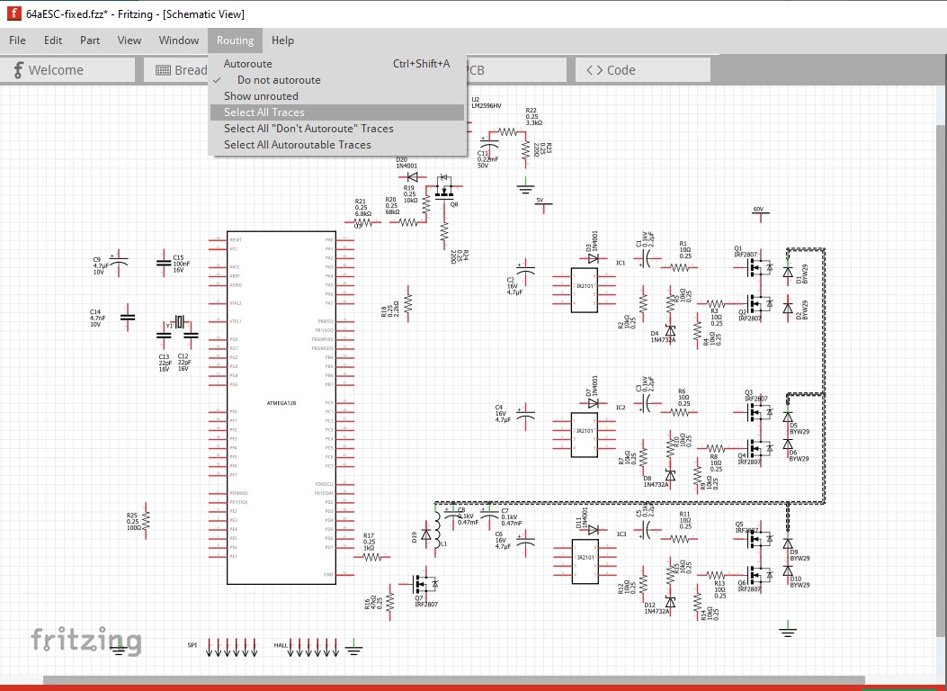
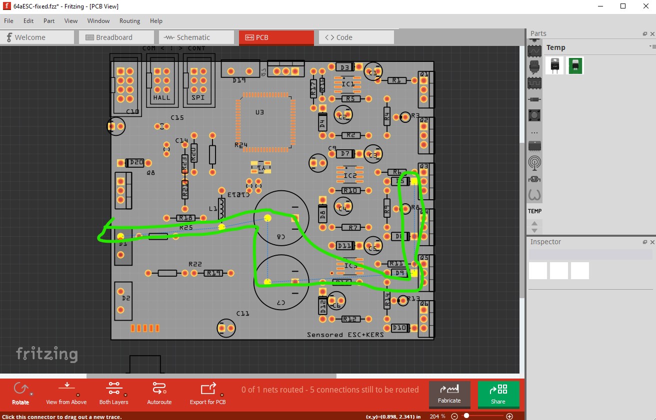
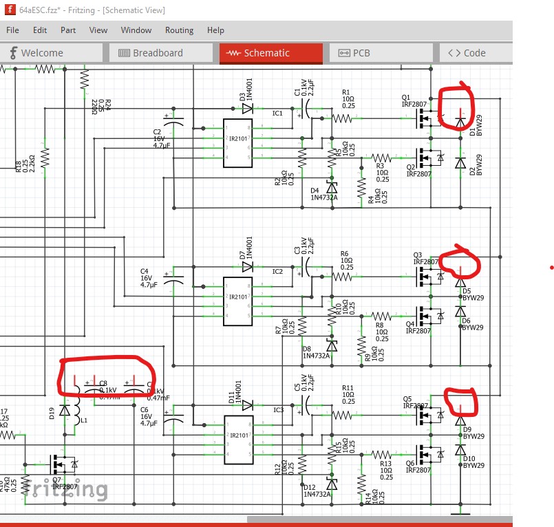
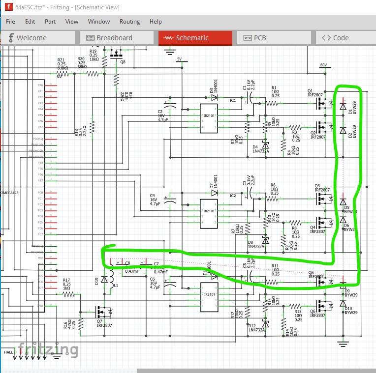
It is looking increasingly likely that this is the bug although I have never seen it manifest this way. Usually there are extra rats nest lines that can’t be deleted. In schematic, I deleted all the wires on the diodes and capacitors which should clear them from the routing data base:
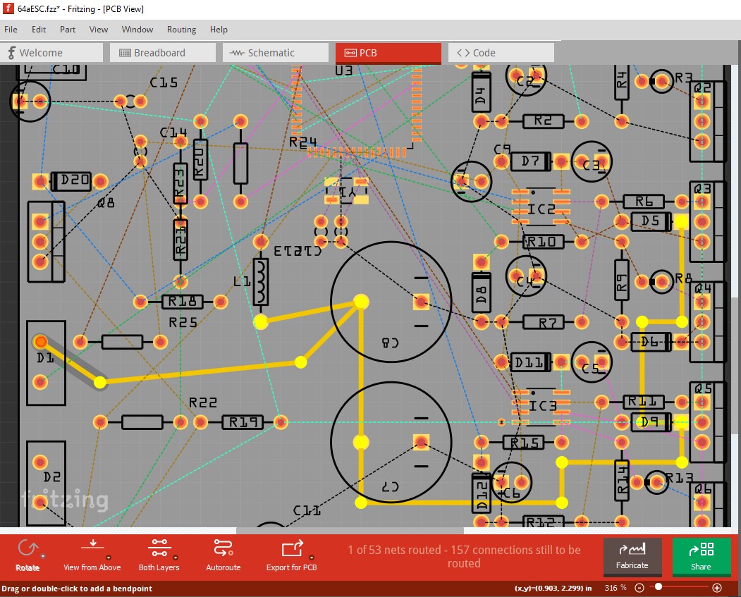
now pcb is routing correctly. This would seem to indicate that this is an instance of the routing bug and the routing database is corrupted and you need to rewire schematic from this sketch (which the above is from)
routing the rats nest lines in schematic creates an apparently correct schematic, although I would not trust it. I would delete all the wires in schematic and rewire schematic making no connections in pcb then check that pcb has the correct rats nest lines as expected from schematic. It is likely the corruption is still present and may re appear later which is undesirable. Note you can start Fritzing twice with the same .fzz file. That allows you to have the current schematic in one window and delete all traces in schematic in the other window, then re run the wires in schematic (by seeing where they connect in the first window) which is somewhat less work. At the end of that save the new sketch as a different .fzz file and use that going forward. Good luck!
Something came into my mind: all these problems started once I started swapping out some diodes for the new package formats in imported fzpz. I wonder if this can be of any help to fix the bug.
Well I guess I got also quite some work for the replacement too … I really should have all the components that requite thick tracks do be all close to each other.
Damn it this is more time consuming then I expected … but no one makes sensored BLDC motor ESC for end users the way I want it … I’ll just have to see this trough till the end if I want all the features.
Is there any plan for a bugfix release ?
Can the bredboard thing be disabled ?
I used an option to delete all the pcb traces leaving just the rats nest lines … I was wondering if the corrupt database can be flushed in a way that just the components and their placement is kept ?
Can I strip all the traces form bredboard, schematic and pcb in a programmatic way ? instead of doing it manually ?
If I list the files in the fzz (wich is reported to be a plain zip file) I get this:
Now appart from the fpz of the custom components and the svg files all that is left is the 64aESC.fz which is reported to be an XML file.
I’m supposing the database is somehow kept in this xml file … I see in there tags which I suppose are related. I guess it could be done manually but I’m not going to edit manually 1.6Mb xml file.
Would it not be better to use a real database like sqlite3 … it would then be easier to write custom database manipulation tools
If the problem is intermittent, it does not seem like a database corruption.
Debug errors without being able to reproduce them it’s extremely difficult. If you can find a way to reproduce the error in a small example, it will help a lot to fix the bug quickly.
I’ll see if I can come up with a circuit that corrupts more predictably … or at least something that allows to reproduce it reliably.
But I’m assuming that if it were to show up in very simple circuits it would have already been fixed.
In any case Peter was able to reproduce the error starting from the fzz I attached above.
Not ‘completely’. Go to each view, on the Routing menu pick “Select All Wires” or “Select All Traces” (depending on the view), then press the delete key (or Delete on the Edit menu). That will work unless something has been locked. If so, before doing the delete for the view, clear “Lock Part” in the edit menu.
Disabled? As in not have that view available? No. But you can ignore it. It will have no effect unless you start adding ‘real’ wires, not just the generated ratsnest lines based on wires and traces in other views.
Depends on your background. There are tools available to manipulate XML content too.
Not quite the way described, but SUPPOSEDLY delete all of the traces in all of the views, then doing a select all in one view, and paste into a new sketch will get close. It will only keep the relative positioning for the specifically copied view. Other views may or may not retain the positioning.
It is PROBABLY possible to delete a section of the XML to do it without the copy and paste to new sketch. Like databases, there can be interrelated pieces that can break when manipulating the lowest levels without knowing enough about how the pieces are being used. I have explored doing some manual z ordering patches that way, but nothing with the net lists.
For bug fixing, first have to identify what the bug is. Incorrect output shows there is a problem, but finding which piece (or multiple pieces) of the code are responsible is not trivial.
While not impossible, it is unlikely. The bug in the past (and it has only been seen 4 or 5 times in the last 5 years) comes when the user makes changes in another view. Unfortunately they don’t know what sequence of changes they made and I have never been able to find the sequence of changes that causes the fault, all I have are examples of sketches were the fault is present. I haven’t been able to figure out how to start from an unrouted set of parts and make the changes that it appears the user made and cause the routing corruption. Unless we can find the sequence of events that cause the problem we can’t figure out how to fix it.
Yes that is very desirable! The paths are likely to be high current, and thus you can get voltage drop across the path (2oz copper instead of the usual 1oz will help too!) As well you want to route all the high current grounds together and only connect them to logic ground at one place to avoid voltage drop in the high current grounds affecting the logic noise margins.
Development has been restarted (it had died for around 4 or 5 years) so there are now bug fixes coming out. I don’t know when the next release is, but this bug won’t be fixed in it because as noted we can’t reproduce it. There was a new case a couple of months ago so I know it still exists in version 0.9.9 unfortunately.
Note at present but if you don’t make changes in it, it won’t cause this bug and so can be safely ignored. If you don’t need breadboard (which is Fritzing’s fairly unique feature) Kicad is an option. It is more complex to use than Fritzing though I think.
Usually (but from the low case count, perhaps not always!) clicking Routing->Select All Traces then hitting the delete key to delete all the connections usually clears the problem in the routing data base leaving the parts placed so the routing can be done again. As I said it is possible that the corruption is however still present since we don’t know what causes it, so the safest option is to start a new sketch but that is a lot of work.
Correct. The .fz file is the external (created by Fritzing) XML representation of the sketch. When the sketch is loaded, the .fz file is read and populates the data base. Unfortunately it populates the data base (Fritzing internally uses sqlite I believe) with the corrupted values. I have looked at the .fz files for the corrupted examples, and it appears that the problem is the wire definitions have been partly (but not completely!) deleted, leaving an incomplete definition of the wire. As noted I haven’t been able to find the sequence of actions in Fritizng that will cause it to do this though. So it seems likely that deleting all traces in all views should clear this problem (and in the cases I have, it had done so) but I can’t say for sure that is true always unfortunately. I would probably do that (delete all the traces and remake the connections) as being the least work, but be aware that it may fail.
I would agree, but in the single case where I managed to get a correct output (where I unfortunately did not save the resulting .fzz file!) I had clicked on the various connections in question in schematic and pcb to check the connections in both views. My guess is that I moved something in schematic (as there were no traces in pcb) that caused the connections to be corrected. That said, when I realized that was a one time thing, I have tried deleting the affected wires in schematic and re doing them, and that does not clear the problem (which is why I think this is an instance of the data base corruption problem which acts exactly this way.) Deleting the connections in schematic and then switching to pcb view and routing them there does work, the correct rats nest lines are made in schematic, but I am not at all sure the corruption isn’t still present and will come back to bite us later!
Well I’ve been dba in my past jobs so making a query is not a problem for me … but I can’t say that correctly parsing XMl has ever worked for me right: since there is no standard in XML apart from the way the tags are opened and closed I’ve never found a parser that does a good job on whatever XML I happen to need to parse at the time.
I must say that is it a waste of cpu time and energy to pase XML load it into a sqlite database … and then parse the sqlite database back into XML … just saving the sqlite database inside the fzz would be so much easier both when saving and when loading.
Taking an educated guess based on my background:
I also assume that the database is not physically corrupt (blocks in the tables are probably consistent) but it is rather a logical corruption meaning that the application wrote some inconsistent data in the database … if proper constraints were in place, specially for the foreign keys, it would probably help find out how and what is corrupting the data (as it would get a an error back from database while attempting to corrupt the data).
Now back to a Fritzing newbie question: is there a correct way to connect to each other 3 or more components on the schematic view ?
In case of 2 components the action is obvious … but when there are 3 or more should one be attempting to join the 3’rd to the connection between the other 2 (at a bend point) or should one try to connect the 3’rd to any one of the other 2 directly ?
I find the python lxml library does a good job (at least on Fritzing XML which is all I’ve used it on!) That is what FritzingCheckPart uses to read the xml to check parts.
Correct, something in the Fritzing code is screwing up and it looks like only partially deleting a wire. That then gets written to the xml file and propagates the error on reload (it loads the partial wire definition which is what causes the error, because some parts of the definition are not present when they should be I think.) I assume (but don’t know because I wasn’t involved in Fritzing when development was still occurring) that xml output was considered more user friendly.
Yes, either start at the pin of one of the parts and drag the wire to the pin of the next part to be connected, or drag the wire to a bendpoint in the existing wire. Don’t drag it to a straight portion of the wire, it will appear connected but not be! If you left click on a pin everything connected to it should light up yellow which will find errors like connecting to a wire not at a bend point.
I do not believe that is what is happening. A sketch only uses xml. The database holds information about the parts. Which are not in a sketch, or copies of which are in sketches, or references are in sketches. Depending of various cases. And those references are to the xml files, which are what will get loaded when a part is added to a sketch. The database is just an index to the part files.
Should. With good constraints, to make sure that a ‘master’ can not be deleted when there are still ‘child’ records. The applications started as a class project quite a few years ago. There were (I expect) a lot of different opinions about what was good/acceptable/apparently working code. As mentioned above, I do not think ‘foreign key’ applies in this context. It is all xml for physical storage. I have not looked into how that is represented in memory, but I am pretty sure that ‘relational database’ is not a good description.
Internally, the wires create a ‘net list’. A list of all of the part connection points that are logically/physically connected together. The wires are part of that. So it should not matter (to the net list) whether a directly wire connects pins on different (or the same) part, or whether a wire connects a pin to a bend point in a wire, which then connects to another pin. I say “SHOULD NOT”. We have seen cases where the rendering can get messed up, so a wire to a bend sometimes looks like it is not connected, even when it really is (the light up yellow test shows it connected, as well as other views). This happens when a part is moved, which automatically redraws wires. Only sometimes. I am told that a recent patch fixed at least some of that.
I think I may know how to reproduce the error:
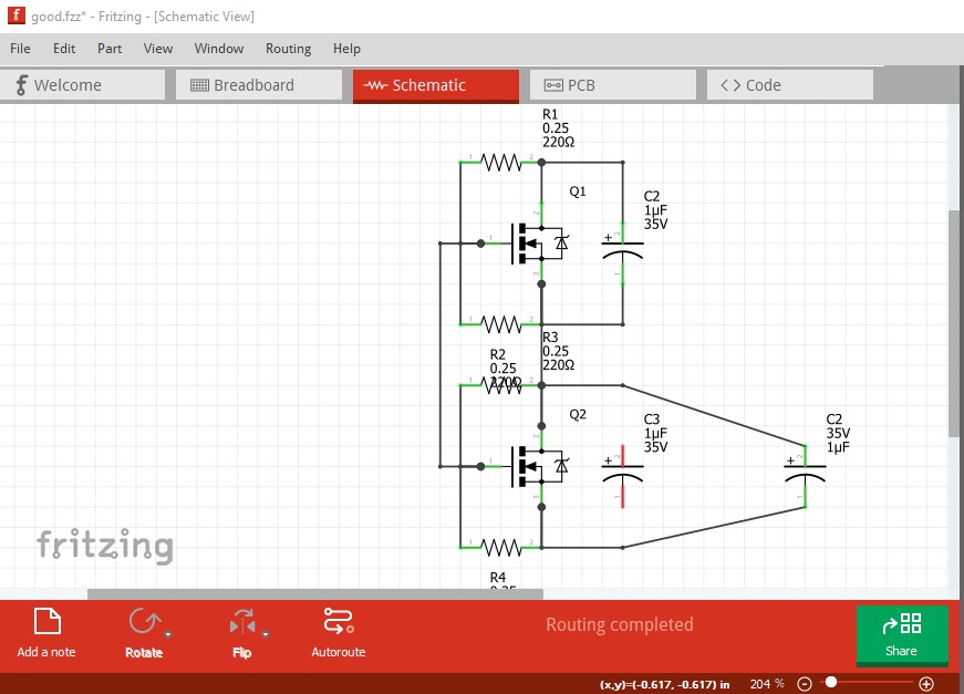
start with a simple circuit like like this: good.fzz (5.7 KB)
Supposing you want to rename replace C3 with a tantalum capacitor while and at the same time rename C3 to C2 and then rename C2 to C1 (from schematic).
But you rename C4 (the new tantalum) to C2 while the electrolytic C2 above still exists, then move the wires from C3 to the tantalum c2, then rename electrolytic C2 to C1.
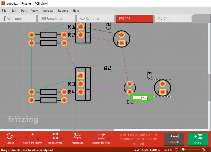
Then look at the pcb rats nest lines: for me they are messed up.
with a uniqe constraint on the componane labels I think this could be avoided.
You ither should not be allowed to cave to capacitors with the same label or the label should be a foreign key to to a unique compoinent id so that you cannot corrupt data by doing clumsy renaming.
I think at some point I did this because I wanted the diodes to have a more logic numerical sequence in the labes and I may have had duplicate labels temporarely on the schematic.
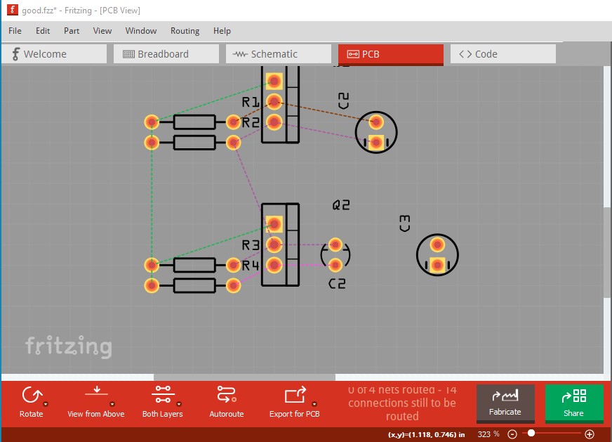
For me this appears to work correctly (although it looks a little odd.) In schematic drag in a tantalum cap, edit its label to c2 and move the c3 wires to it:
Note the tantalum cap is different in pcb than the electrolytic the bar on the bottom is the positive terminal where it is negative on the electrolytic so you need to rotate it 180 degrees to make it the same as the electrolytic. The rats nest lines take the shortest path to the net (electrolytic C2 minus in this case) so the rats nests look different in this case. Flipping it and moving it closer to Q2 restores the original layout as far as I can see.
From the examples I have seen in order to get database corruption you need to make a conflicting series of changes (and the exact sequence is unknown) in another view. I.e. with a circuit fully routed in schematic, make changes that conflict (i.e. create new rats nest lines in schematic that didn’t exist before) in pcb. At that point sometimes even removing the changes again won’t clear the rats nest lines in schematic again (other than deleting all traces in all views.) That doesn’t seem to be what is happening here (although you are correct, Fritzing shouldn’t be letting you edit the label to something already in use on another part!) Are you seeing something different than what I show above? I would love to get a repeatable reproduction of this problem!
If you only need to ADD to the schematic, you do not need to delete the pcb traces first. You only need to delete pcb traces if they are ‘wrong’ for the changes to be done to schematic. Simplest is to delete all traces, but if the changes are small, specific traces can be deleted instead of everything.
You do not need to start with schematic. Some start with breadboard instead. The ‘rule’ is to do all of the wiring in a single view, then use (only) ratsnest wires when routing the other views.
Regular saves to go back to are always a good idea.
Well starting on breadboard is perfect for the simpler projects … but most of them can then be taken to perfboard without needing to manufacture a pcb.