PCB routing issues

Hi everyone, I’m new to electronics and fritzing, I got involved as I’ve rebuild a 1970’s Lister SR3 generator and required a control panel to help run it. This would monitor two thermisters, DCvoltage and AC voltage with certain conditions it would activate various solenoids to control fuel flow as well as start/stop solenoids, the temperatures were to act as protection against over heating.
Working for several weeks on the programming and learning how to master and slavbe two arduino’s due to problems with theAC side of the program i finally got it work.
I need to draw the circuit and PCB.
I constructed the schematic and PCB a piece at a time, working in both views so as to position
the components and check traces etc.
finally got everthing in place and used the auto route to connec the PCB only to find that it connect the 12V side of my lm7805 to the 5V side and totally misses out the other one from connecting to the slave arduino, even when I connect them manually and then deselect the donot auto route option it still replaces the links
has anyone else had this problem or am I doing things wrongschematic

I had visions of creating the designs and ordering the PCB, now I have serious doubts about the viability of the board.


Version 0.9.4
(CD-498-0-a1ffcea 2019-12-01) 64 [Qt 5.12.3]
windows 7 pro

Please also attach any files that help explaining this problem![pcb|690x326](upload://9Np![pcb|690x327]

You probably did something wrong and forced different connections in different view. Basically only work in one view and trust the ratsnests in the others.

Upload the fzz with the 7th button in the reply.

Hi ,I thought I had put the PCB view on as well then couldn’t find a way to edit,sorry Here it is


As you will see there is a link between 12DCV + and the LM7805 5 V output but then you follow the %v output and it goes nowhere, it keeps giving ratnest sugestions but then connects then somewhere else

Were flying blind without the fzz file, so you’ll just have to disconnect the connection.

is this the file your asking forcontrol_box_version2.fzz (113.2 KB)

Yes that is the file. The complete sketch document.

I do not understand what you mean by the %v output goes nowhere. Fritzing will highlight (in brighter yellow) vall of the connectors and wire ends it believes are connected together (into as single ‘net’) when you click and hold on any one of the connectors. Here are snapshots of what that looks like for the 12V input, GND, and each of the LM7805 regulator outputs. Without a full analysis, it look like power and ground are connecting to reasonable places.


This is definitely not a ‘finished’ board yet. On the Routing menu, Click Design Rules Check (DRC). That reports (and shows with red overlap markings) several places where the traces got too close to, or even overlapped with, some other trace/connection, which shorts them together. Some of that may be from autorouting. It is not very smart, and can ‘cut corners’ a bit too close. Others look like manually placed traces that were not properly routed to avoid connectors.

I believe that %v was meant to say 5V.

What makes you think the 12V is connected to the outputs of the 7805. Click on the 12V pin of the header and look at which pins on the 7805s light up. Now hover the mouse pointer over those pins, and it says inputs.

Also never use auto-route as it makes a mess, as can be seen in your sketch. Pros set the grid and always manually route, like below, because AR’s can’t do this

Watch the tutorials and it will give you basic ideas on how to layout stuff.

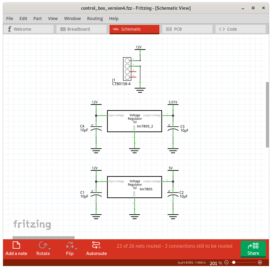
Right duh. “%” is shifted “5” on most keyboards. A simple typo. My comments and images still apply. There is no link shown between the 12V net and the regulator 5V output net connections, and the 5V lines from both regulators seem to be going to reasonable places.

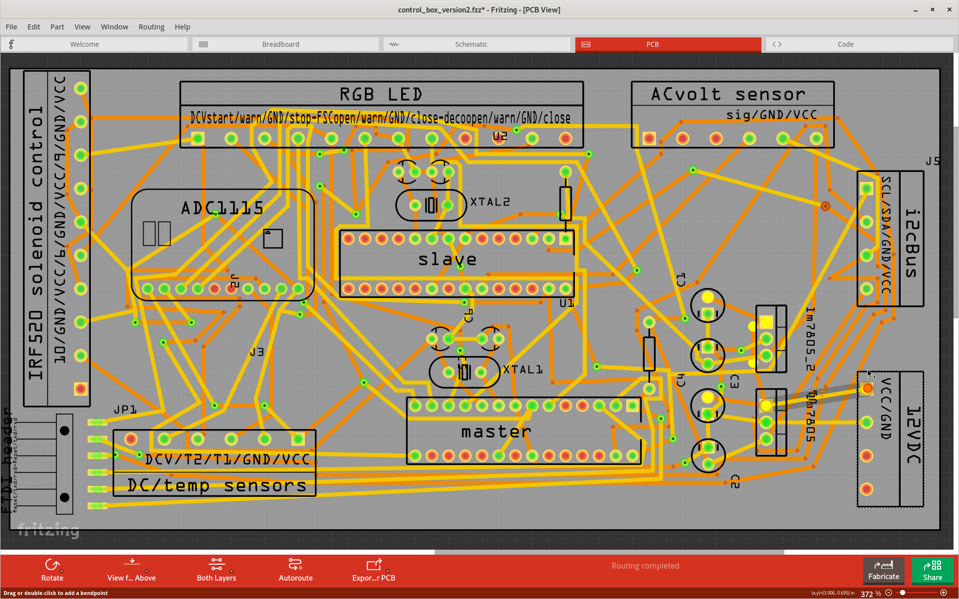
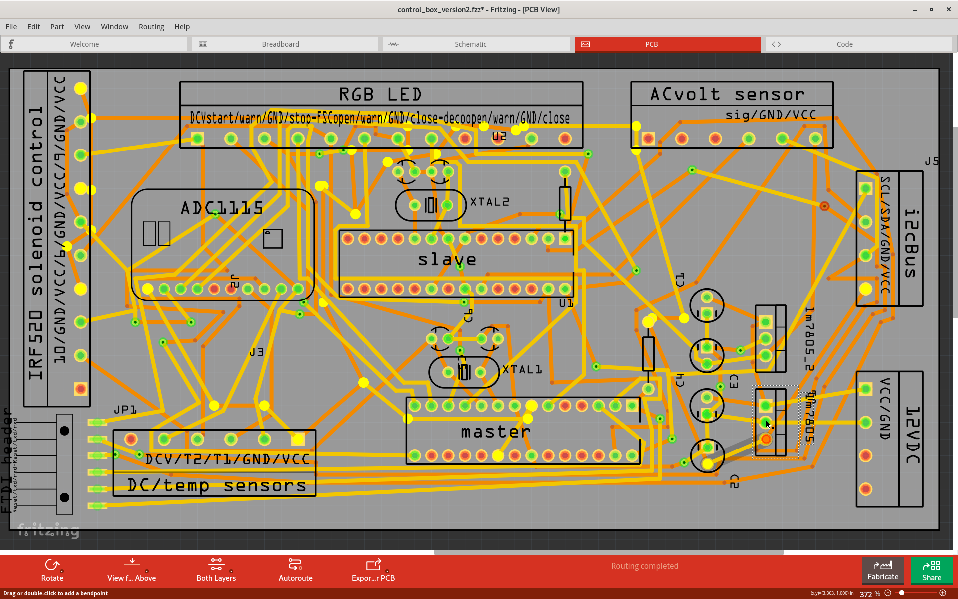
I wouldn’t say “never”, but when using it, be prepared to do a lot of manual cleanup of the result. It won’t take much practice to get cleaner routing manually than what auto-routing generates. Cleanup up the mess that auto-routing makes can be the start of that practice.

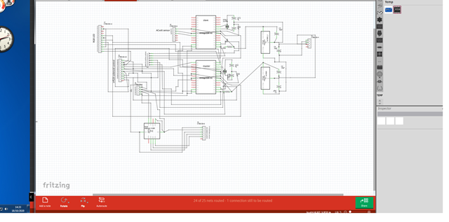
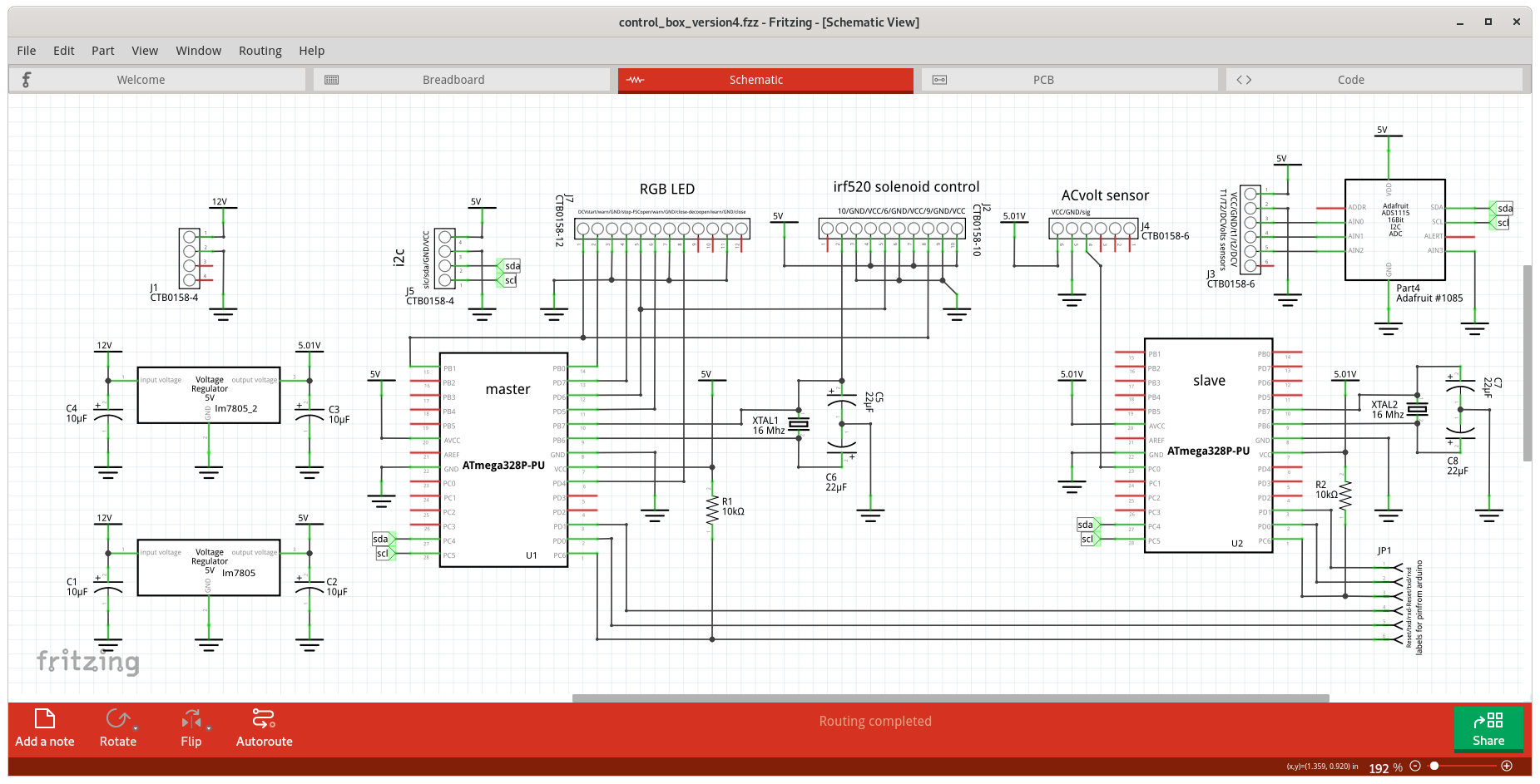
The schematic view is (also) rather messy, and a lot more difficult to follow than it needs to be. From the brief description, you have been editing and making changes quite a lot to get here. You should (fairly regularly) cleanup to simplify the layout and routing. None of this is analysis how your circuit works. Just how it is presented on the schematic.

One thing that can quickly reduce the clutter, is replacing all of the ground wires with the standard GND symbol. Instead of running actual wires between components, just place GND symbols at convenient points, and connect to them. All of the GND symbol are connected together by invisible wires. The same works for power connections. There is a standard Power (V++) symbol that can replace the majority of the power rail wires. Your circuit makes that one a bit tricky, because you have 2 separate voltage regulators outputting the same voltage, but not on the same rail. That can be ‘fudged’ (in Fritzing) by setting one set of the power symbols to a slightly different voltage. All of the ‘Power’ symbols set to (exactly) the same voltage are connected by invisible wires. With that, one way to layout the power input and regulation section of the schematic would be.


Incorporating that, and moving parts around, here is what the circuit around the slave microcontroller could look like.

Power and GND are not the only possible symbols that can be used to electrically connect distant pins. There is a generic “Net label” part. A pair (or more) of those with the same label are connected by invisible wires. Very useful for tying pins to a common bus, like I2C. Adding net labels named “sda” and “scl” for each connection to I2C simplifies the schematic wiring diagram. When using the net labels (or power symbols), it can be easiest to place one generic part, change the label, then duplicated it as many times as needed. Instead of placing the generic part, and changing the label, each time. After some more adjusting, to group parts, and reduce visual interference between wires, I ended up with this.

This is not ‘perfect’ (or professional), but it is (to me) a lot easier to understand how the pieces interact. One of the things to improve, is the labeling. A single string with the names for all of the pins on a connector is simpler, but does not stay lined up very well. With a couple hints from some of the text, the labels are referencing Arduino (UNO) pins, but the schematic is using the raw microcontroler parts. I assume because the circuit was breadboarded using Arduino boards, not the chips, and that was an aid to keep the wiring straight.

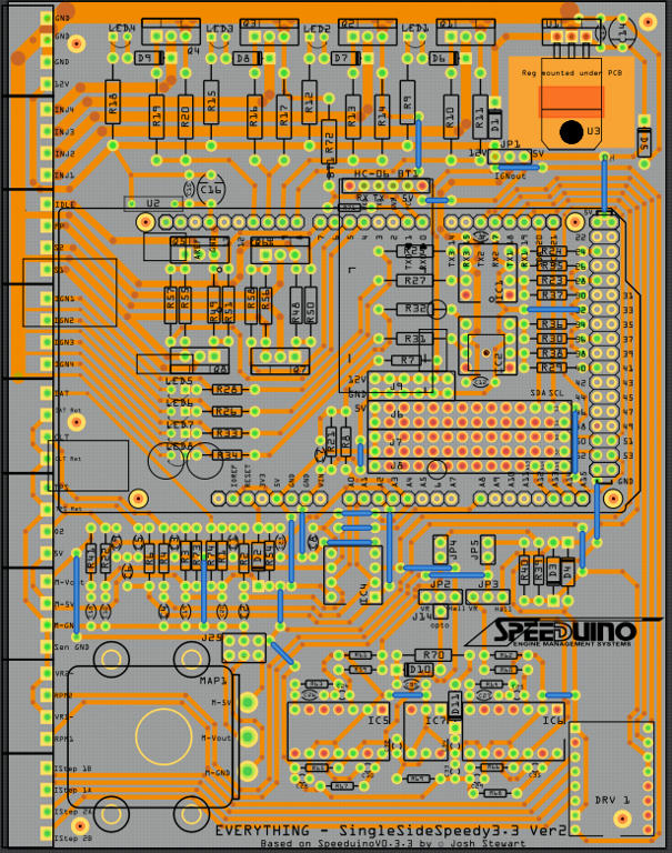
As @Old_Grey said about the PCB, there are tutorials around that can help fill in the concepts, guidelines, processes to use to get more readable layouts.

Some people do sudoko, crossword, jigzaw puzzles. I play with layouts.

Similar cleanup could be done with the breadboard view. Breadboard view would also benefit from using the breadboard part to place the raw components on. It is not used (or needed) as often on schematic view, but on breadboard view, setting the color for individual wires can make tracing the circuit easier. Black for ground, Red for power rails, a colour for sda, different for scl. More colours, with and without banding, for other data lines.

1 Like

Hi sorry for the later reply, Thank you very much for all the comments and pointers, I didn’t know you could lay the drawings out in the way shown, I shall spend several days reading through this over and over and putting into practise your sugestions. Many thanks once again you’ve been extremely helpful and patient.
Stay safe
Barry