:Hi everyone!
First at all let me introduce myself: My nickname is Namirie and I’m from Spain. I would like to categorize myself as an electronic and technology lover and selflearner.
Few years ago a business idea came to my mind and few months ago I started to develop it (COVID lockdown was great for this).
In my project I would like to have some arduino stuff implemented on it so I started practicing and reading info on internet about electronics, 3d printing, prototyping… So suddenly I decided to move from prototyping to manufacturing. Downloaded Fritzing and I started doing some basic stuff with breadbords and schematics. Few days ago the idea of PCB making came to my mind and this is where my doubts appeared.
For this particular project I´m using 4 MFRC522 RFID readers that communicate with each other and Arduino using SPI bus, after lot of hours triying I managed to get the 4 readers working at the same time. This is my schematics:
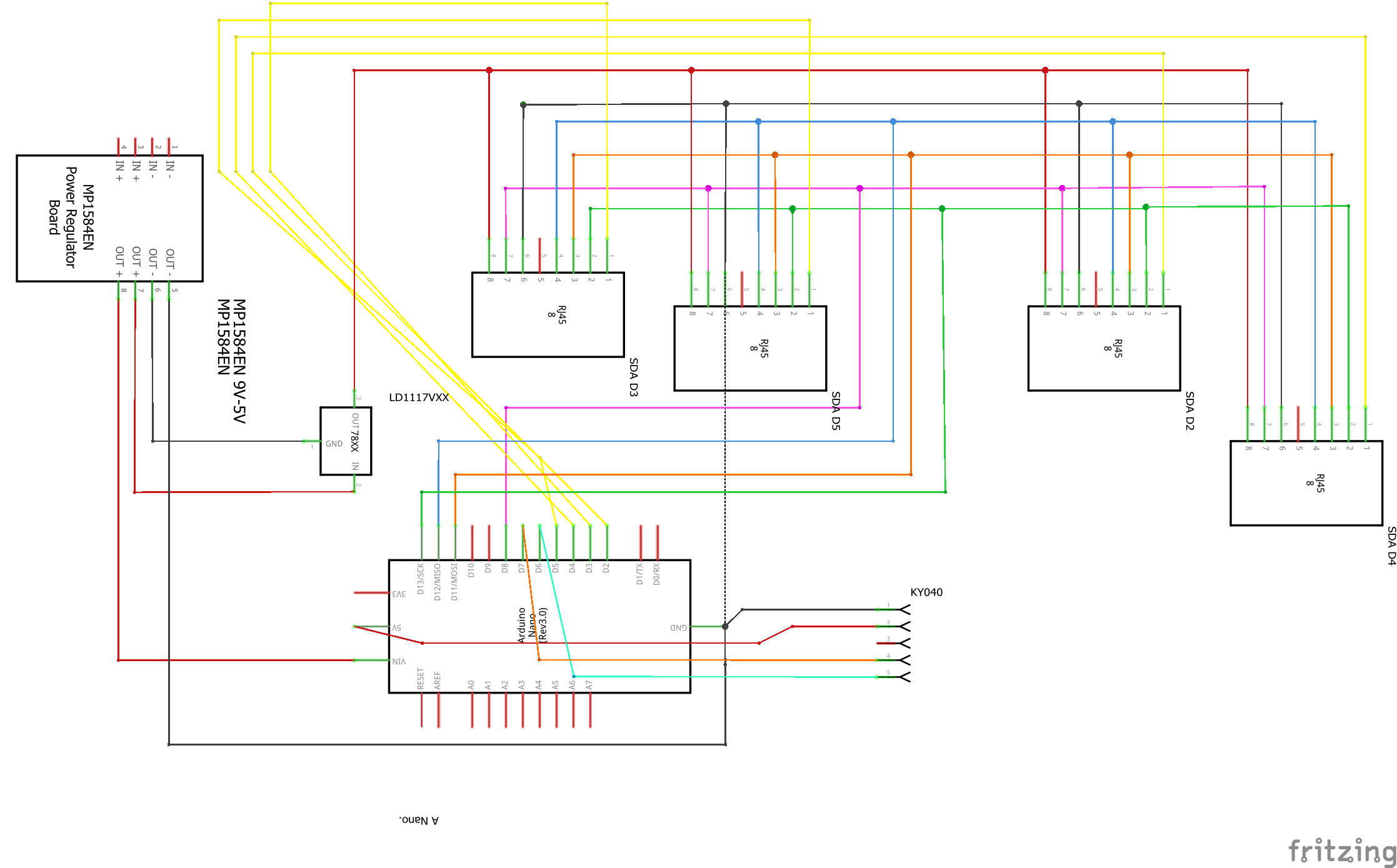
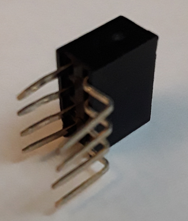
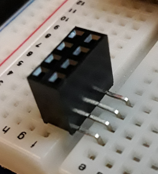
I know that it seems to be a little bit messy but let me explain it to you: Basically, there is an arduino nano connected to 4 RFID readers, PSU is connected directly to a voltage regulator to supply 5v to arduino and 3,3v directly from PSU to MFRC522 Readers GND and 3,3v Pins. I`m sure some of you will ask me why im not using level shifers for the SCK, SDA, MOSI and MISO pins when Arduino supply 5v over them, the reason is that after several tries i figured up that some of them can work properly without the level shifters so I´m avoiding using them. Also, as you can see in the schematics im using RJ45 connectors to wire up the readers in a more convenient way.
Despite the other components in there I dont want you to lose your time with more details, my main doubt is making this schematics in PCB:
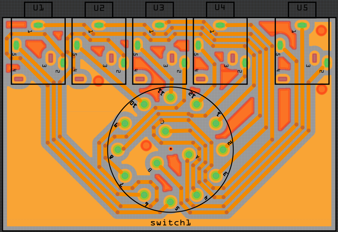
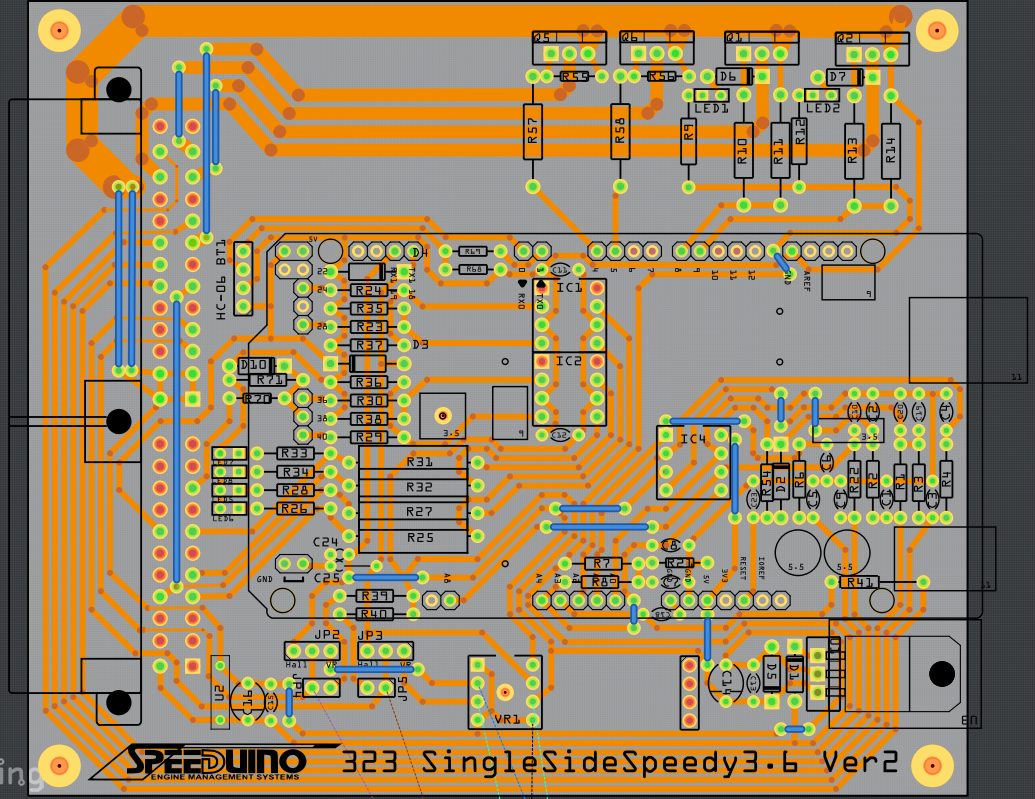
First problem i found is that as Im managing paralel connections the wiring was a nightmare so i adapted it to a 2 layers PCB and some jumpers between them when i couldnt avoid crossing wires.
After several hours triying it out, i finally managed to get a “well done” PCB, Im still a beginner so i wanted to ask you if the following PCB is actually good to send to the factory or you guys expertices would change something on it.
EDIT: Seems like new users only can upload 1 image and 2 links… /sad.
Please note that first image is both layers, the second one is just the first layer and the last image is from the last layer in PCB.
I know it has been a long post but i wanted to give you guys as much detail as possible. Thanks for reading, for your time and patience. Any help would be appreciated.
Thanks in advance and kind regards,