PCB (Board) Cutouts and Creating It - Simplified

I Discovered Some ‘Magic’ regarding making the Board’s SVG :grinning:

Summary: A simple way to make the Board with Cutouts (and silkscreen) that appears to play well with Fritzing.

I read the SVG1.2 specification to better understand what Fritzing wants - Here’s my take on it:

After reading Fritzing info and importing & exporting many SVG’s into/from Fritzing to gain understanding, I discovered some ‘Magic’ that seems to work perfectly well, repeatedly!

Point 1:
Fritzing info suggests using a Layer called “boardoutline” for cutouts. However, no matter how it’s elements are crafted, differenced, subtracted or path’d, it never consistently worked (for me).

Point 2:
Loading a very basic SVG (with my Hand-coded svg (noted in my replies to this post). ) worked fine. Then, exporting an SVG image from Fritzing, revealed the exported file gets updated to include a “boardoutline” layer.

Point 3:
I created a new SVG (using Gravit) that has the recommended Layers (silkscreen, board and boardoutline).
I did NOT do any Boolean (diff, subtract…) or Pathing. I simply created the elements and exported as SVG.
Also included two silkscreen shapes.
NOTE: the one ‘Path’ item shown in the Layer panel is a ‘Freehand’ drawn Path (not an element converted into a Path).

Loading the file into Fritzing for the PCB resulted in a ‘Magical’ outcome! :joy:

All elements intended as Cutouts worked including those with tiny features such as Rectangle-Width = 1px and Radius of 0.25px. Hard to believe!!!
Proximity to other elements no problems!! Silkscreen worked too

I want to underscore: No Paths, No Difference, No Subtraction…
In fact, it will work with only a board>boardoutline layer!

Below shows the various elements in Gravit, Fritzing and the exported Gerber Contour file.

The Gerber with All the cutouts (and board shape) easily imported into CopperCam (for creating CNC Gcode).
[ADDED] Also shows up correctly in a Geber Viewer…

This is good news, because I’m getting nowhere with making this work :slight_smile: . Could you upload the svg that created this please so I can try it out and see if I can make it work?

Peter

Attached. First thing you’ll notice is that it’s drawn in px and is small - because I wanted to test interferrence’s of elements by crowding them. Overall size results in ≈22mm

Multiple_cutouts1wFreehandPathwSilk.svg.fzp (3.6 KB)
Boardoutline_Test.fzz (2.1 KB)

Thanks, I’ve been trying with the svg in inches (to avoid the guess the resolution problems) and haven’t been manged to make it work. My output is more by picasso than anything useful :slight_smile: . Was just going to switch to px and see what that did. I’ll start from here because the result sure looks good! It would be nice to have something that worked dependably for this, and if we can identify the bugs we may be able to fix them now development is running again (although knowing nothing about the gerber code that will probably be hard!)

Peter

I changed a copy of the file to Inches and set the board to 4" x 4".
Moved and resized a few of the items.
Exported it and loaded into Fritzing.

Result - good! Image attached along with the svg.

Multiple_cutouts1wFreehandPathwSilk_INCH.svg.fzp (3.8 KB)

NOTE: I did not scale the file to account for Fritzings 90DPI. I left it at 72DPI.
Thus, looking at Fritzing’s inspector, you’ll see the board is 81mm (which is: 4x25.4 / (90/72)) and is correctly scaled.
The SVG correctly exported with converted units of PX for the board and, interestingly, the Silkscreen shows inch dims and the converted PX.

All is good…

InkScape…

I opened an older file I did in Inkscape.

I did NOT change anything previously done with it.

I added a sub-layer to the Board layer (thus, now having a ‘boardoutline’ layer).

I simply added two rectangles and one circle to it and saved as plain SVG.

Loaded it in Fritzing and Bingo! Contour Gerber below… Inkscape file attached

testINK_wboardOutline.svg.fzp (4.7 KB)

Didn’t want to go too overboard with this but, I did want to complete it by verifying two things:

  1. Is making Text (OCRA) into a Path necessary?
    – answer: YES, otherwise it won’t properly scale font size.

  2. Is making a board perimeter (drawn with lines, versus using a rectangle) into a Path necessary?
    – answer; NO, it works as drawn - perhaps because drawing connected lines in Gravit is done with Bizer draw tool that, in itself, is a Path.

Results in Fritzing atached. I did not fuss with aligning things and making it pretty…

Regarding Inkscape… and Cutouts…

I wanted to see if repeating the “Simplified” approach when using Inkscape would work as well as when using Gravit.

Answer: Yes & No

The “No” is: when making small Rectangles with, or without Radius’d corners.

The “Yes” is: making the small Rectangles with, or without Radius’d corners into a Path.

The issue seems to be related to: Size of the shape. The Large and Tall-Skinny Rectangles did Not need to be Path’d but the Small Rectangles Did Require Path’ing (with or without radius corners). Shapes like elipse’s also require Path’ing.

NOTE: Perhaps an issue Only with Mac/OSX but, I noticed the Layers were not always being properly exported in the Inkscape svg.
Digging into it, I discovered that, ‘Dragging’ to move the layers via the XML panel would not work. Period. They Temporarily looked correctly Indented but, it was only a ‘momentary’ thing that was not saved.
However, using the Menubar|”Layer>Move_Selection_to Layer” did work to properly save.

90x60_R1.svg.fzp (7.9 KB)
smallSlot.fzz (2.0 KB)


I’ve been distracted on another project for a day or two and just got back to this. I have already discovered that as usual I can make this worse but so far better is eluding me. I see there are translates in testINK_wboardOutline.svg so I removed them. That indicates the translates are an issue because the result is that Fritzing now matches the contour.gml file (i.e. the text is the wrong size and in the wrong place) but that isn’t the desired direction :slight_smile: . I’ll continue poking at it and see what I can figure out.

Peter

Interesting…

I see there aren’t any ‘Translates’ in the Gravit svg but I do see them in Inkscape’s svg.

I didn’t dig into it because I don’t like Inkscape and won’t use it for Real Work - partly because I don’t like it but, also because they stopped updating it for Max/OSX (perhaps they’ll figure out the issues). Thus, my version is outdated. Current Stable is 0.92.4 but, for Mac, it remains at 0.92.2.

I can appreciate wanting to use Inkscape as that’s what was used for Fritzing’s part/pcb files. But, with shortcomings of it for the Mac, and having better-working app’s such as Gravit (even with it’s shortcomings not yet fixed [such as “vector-sizing” not fixed], it seems the “lesser of evil’s” for my needs and sets me up as a Happy Camper :smile:

Inkscape release info…

Interesting! I wasn’t aware that Ink was not up to date on the Mac. There is a major new release of Inkscape in the works (1.0), but the dev snapshots are pretty broken, much of xml editor and scaling aren’t working correctly. It is possible all the effort is going there at the moment. I started a test part from a generic IC (because it is scaled properly) and added some text in silkscreen with lines on the top an bottom of the text to judge if the font size is correct. That looks fine, and I was about to add a slot to it, and realized I can’t (AFAIK) add a slot to a part only the board as a whole. It is desireable to be be able to do this in parts (for instance connectors that need slots), but perhaps not yet possible. Here is the test part as a standard gerber (no cutouts):

and then the testINK_wboardOutline-no-tran.svg (the original with translates removed) with the test part loaded. Note the IC part of the silkscreen is lost but IC1 is still there, and the left borders are truncated.

As well Fritzing is reporting no cutouts detected, but is obviously creating the cutouts which is odd. I’ll continue poking at this and see if I can figure anything out. I remember seeing a reference to “look at this example file for how to do this”, so I’ll try and find that and look at the example file to see if that tells me anything.

Edit: I’m admitting defeat :slight_smile: , I can’t make this work at all. Reviewing previous posts, the theory was that the same path needed to be in all two or three groups (board with the path id boardoutline, silkscreen (with fill and stroke reversed) and optionally silkscreen0 for the bottom layer (although I don’t know why either silk is needed). Your tests indicate much of that may not be true though. I don’t think (but there is zero documentation that I can find on what is and isn’t supported except additive and subtractive paths of which there should be only one being implied but not stated) on what is or isn’t supported. That said I don’t think they intended to have text on the silkscreen. I think the way forward is to make this a feature request to support this functionality in parts (which will require a code change), because that is where it would be most useful (although perhaps hard, which is maybe why it was done this way.)

Peter

Couple of things:

  1. Yes, probably not intended. But, as with many things, Work-arounds can often be the trick.

  2. Cutouts can be done as Fritzing intended (there is documentation on this) However, my Simplified approach seems to work better than the intended way. Though I show in my examples the cutouts with a Color-Fill, I did that only to indicate graphically. I could have made the Fill Alpha=0 and displayed the Borders. Too lazy for demo’ing it…

  3. I have US Patents on some Connectors and take a keen interest in Connectors :rofl: So, would be nice to have an expedient way of doing it (have needed to do that in CAD so, my approach is a step forward in that regard).

The Dummy Way: Only way I’m able to make the Final Result having Cutouts is to make the cutout in the PCB at the desired location. It’s a work-around requiring some fussing to get desired location…

Can use Fritzing’s position feature or my Woof app to get location.

Regarding the Panel indicating No Cutouts: I have had success getting it to identify and list them. But, beyond it’s listing it, there appears to be No need to strive for it as it appears to have Zero affect on anything other than informing user.

The way to get them recognized is Fuss with Boolean, Stroking and Path’ing them until successful. I don’t bother as it was always a ‘Hit & Miss’.

[EDIT - ADDED] Of course, you can use a New Sketch with your custom designed Part and, when wanting to use it as a ‘Faux’ part, simply start a new sketch and design your other stuff (leaving space for your part) then, open the Saved Sketch with your Faux Part and Paste it into the New sketch, delete the PCB from the New sketch and use the PCB from your Faux part. Naturally, move and resize it as needed.

Although this Example does exactly that, it doesn’t use a PCB with cutouts but, that’s a simple matter of using one with Cutouts for your Faux part… Look for the Last Video in my post…

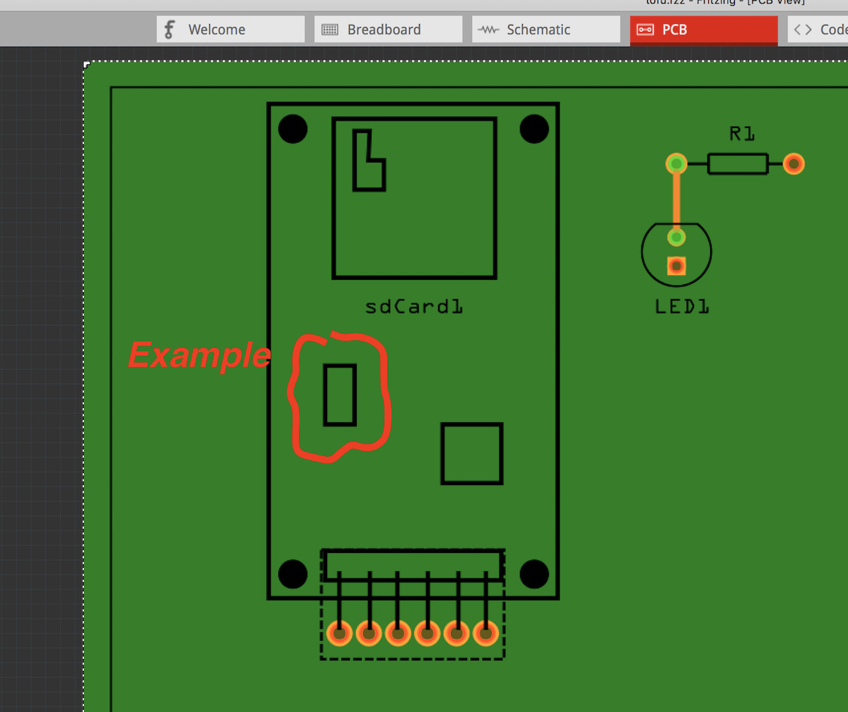
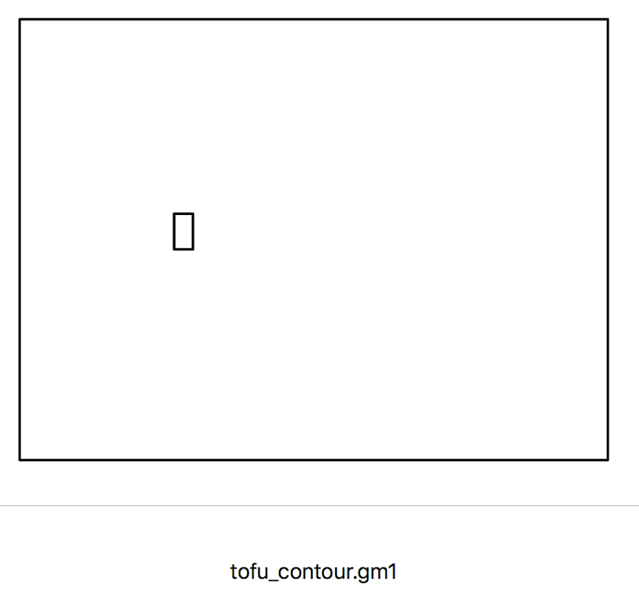
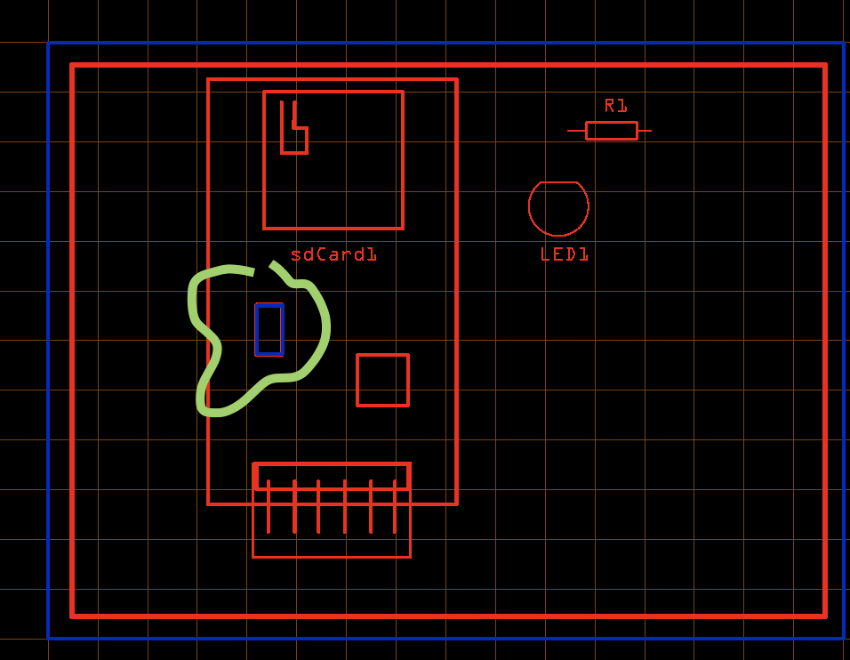
Example Attached is my dummy way of doing it… with image of the Contour and Silkscreen files over-layed (offset by ≈1px for Visual Indication).
It uses my sdCard Part on a PCB with a Cutout for this example…

tofu.fzz (14.6 KB)

[Peter] In case you’re interested in confirmation of Successful recognition of Cutouts… Attached

Real_Cutouts.fzz (1.6 KB)