TE Connectivity Power Relay
no serious problems, the part works as is but a few issues that trip warnings from FritzingCheckPart.py:
Warning 28: File
‘part.relay_te_aa10240f003b068f007356777d31d9fd_2.fzp.bak’
At line 80
name COIL present more than once (and should be unique)
Warning 13: File
‘part.relay_te_aa10240f003b068f007356777d31d9fd_2.fzp.bak’
At line 132
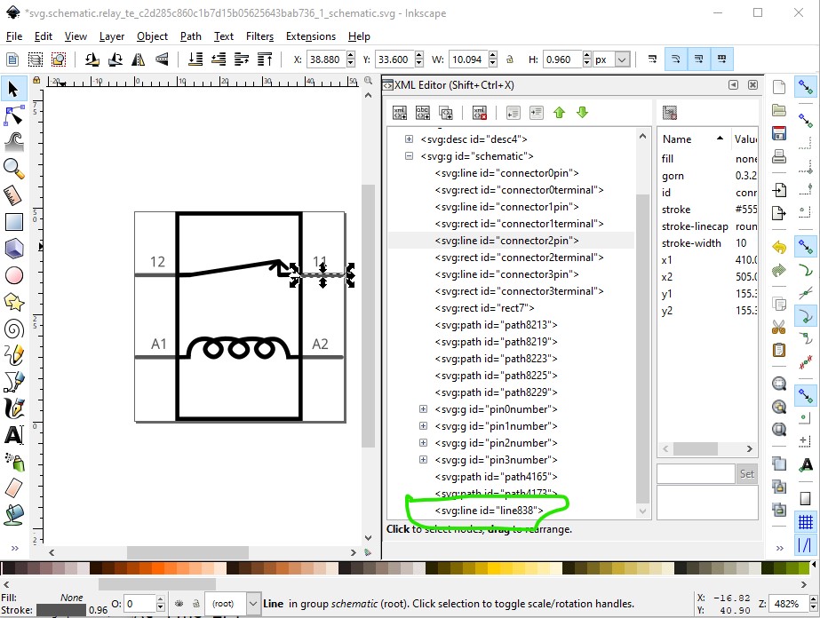
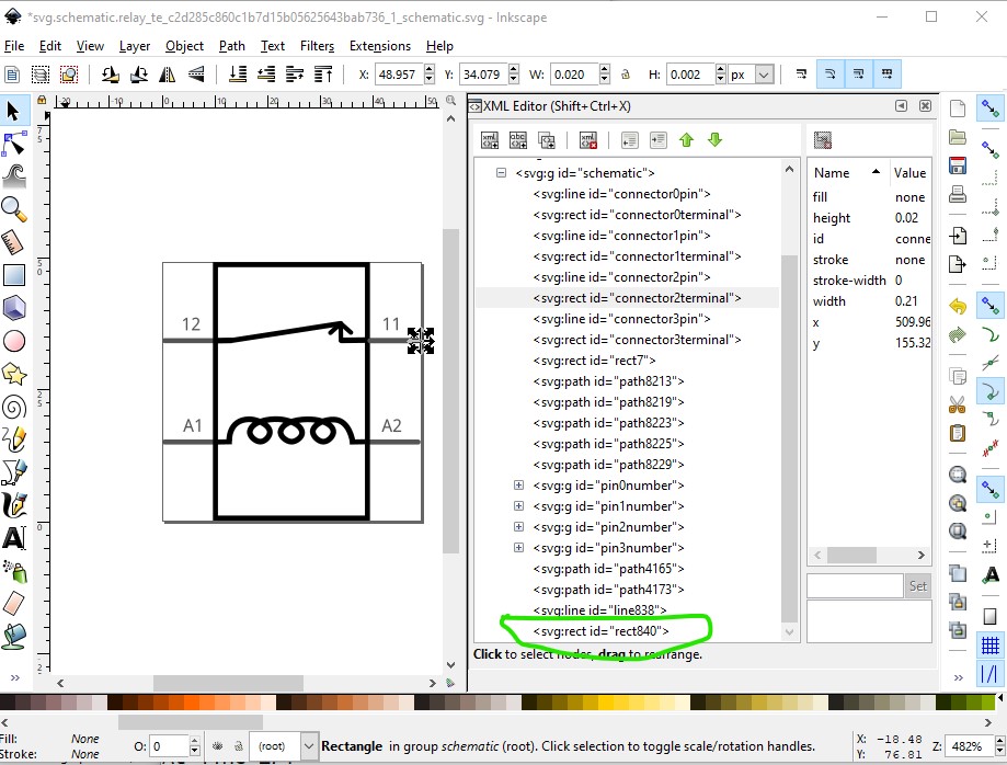
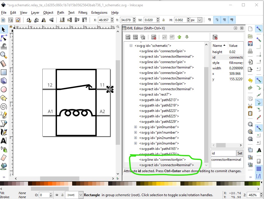
Value connector2terminal doesn’t match Id connector4. (Typo?)
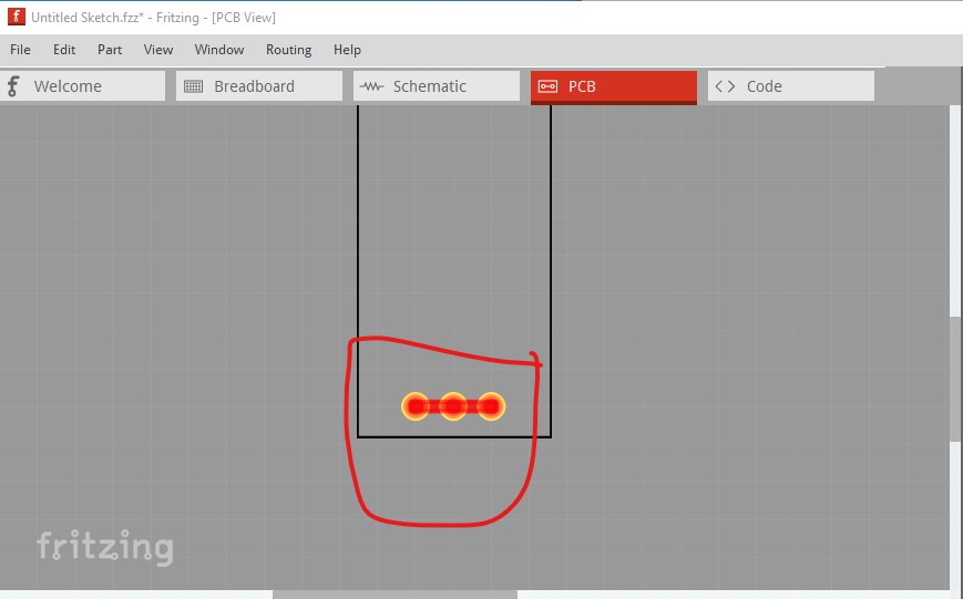
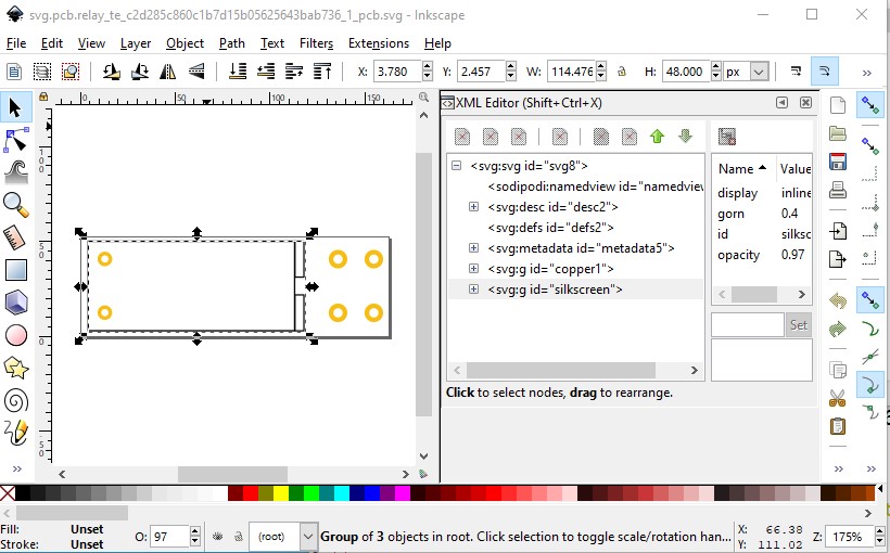
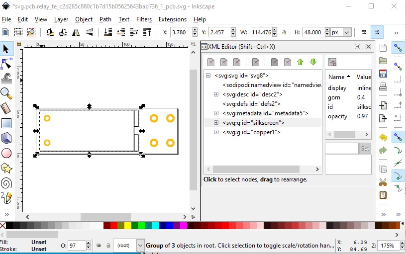
Warning 25: File
‘svg.pcb.relay_te_c2d285c860c1b7d15b05625643bab736_1_pcb.svg.bak’
At line 26
Silkscreen layer should be above the copper layers for easier selection
in pcb view
Error 18: File
‘part.relay_te_aa10240f003b068f007356777d31d9fd_2.fzp.bak’
Connector connector0terminal is in the fzp file but not the svg file. (typo?)
svg svg.breadboard.relay_te_c2d285c860c1b7d15b05625643bab736_1_breadboard.svg.bak
pcb svg change
to
If silkscreen is on the bottom, select in pcb view will select silkscreen which is rarely what you want to do.
Value connector2terminal doesn’t match Id connector4. (Typo?)
indicates the pin in schematic doesn’t match the connector definition. While this works as is, it is confusing. A better solution is to duplicate pin2 and define it as connector4pin like this:
and then connector2terminal
and change the Ids to connector4pin and connector4terminal
do the same for connectors 5, 6 and 7 (using pin3 as the base for pins 6 and 7) then in the .fzp file
    <connector type="male" name="COIL" id="connector1">
  <description>A2</description>
needs to change to
    <connector type="male" name="COIL-A1" id="connector1">
  <description>A2</description>
so the name is unique (in some circumstances Fritzing uses the name field as an index and thus the names need to be unique!) Do the same for all the other names (append their pin number to the end.)
 <connector type="male" name="NC" id="connector4">
  <description>Normally Closed</description>
  <views>
    <breadboardView>
      <p layer="breadboard" svgId="connector4pin"/>
    </breadboardView>
    <schematicView>
      <p layer="schematic" terminalId="connector2terminal" svgId="connector2pin"/>
    </schematicView>
needs to change to
<connector type="male" name="NC" id="connector4">
  <description>Normally Closed</description>
  <views>
    <breadboardView>
      <p layer="breadboard" svgId="connector4pin"/>
    </breadboardView>
    <schematicView>
      <p layer="schematic" terminalId="connector4terminal" svgId="connector4pin"/>
    </schematicView>
to match the changes to the schematic svg. Same for connectors 5 to 7.
connector0 doesn’t need the terminalId in breadboard (as it is not in the svg)
<connector type="male" name="COIL" id="connector0">
  <description>A1</description>
  <views>
    <breadboardView>
      <p layer="breadboard" terminalId="connector0terminal" svgId="connector0pin"/>
    </breadboardView>
to
<connector type="male" name="COIL" id="connector0">
  <description>A1</description>
  <views>
    <breadboardView>
      <p layer="breadboard" svgId="connector0pin"/>
    </breadboardView>
Fritzing defaults to using the pin if the terminalId isn’t in the svg, but this cleans up the complaint in FritzingCheckPart.py (and is more correct!)
TE Connectivity Power Relay-improved.fzpz (8.8 KB)
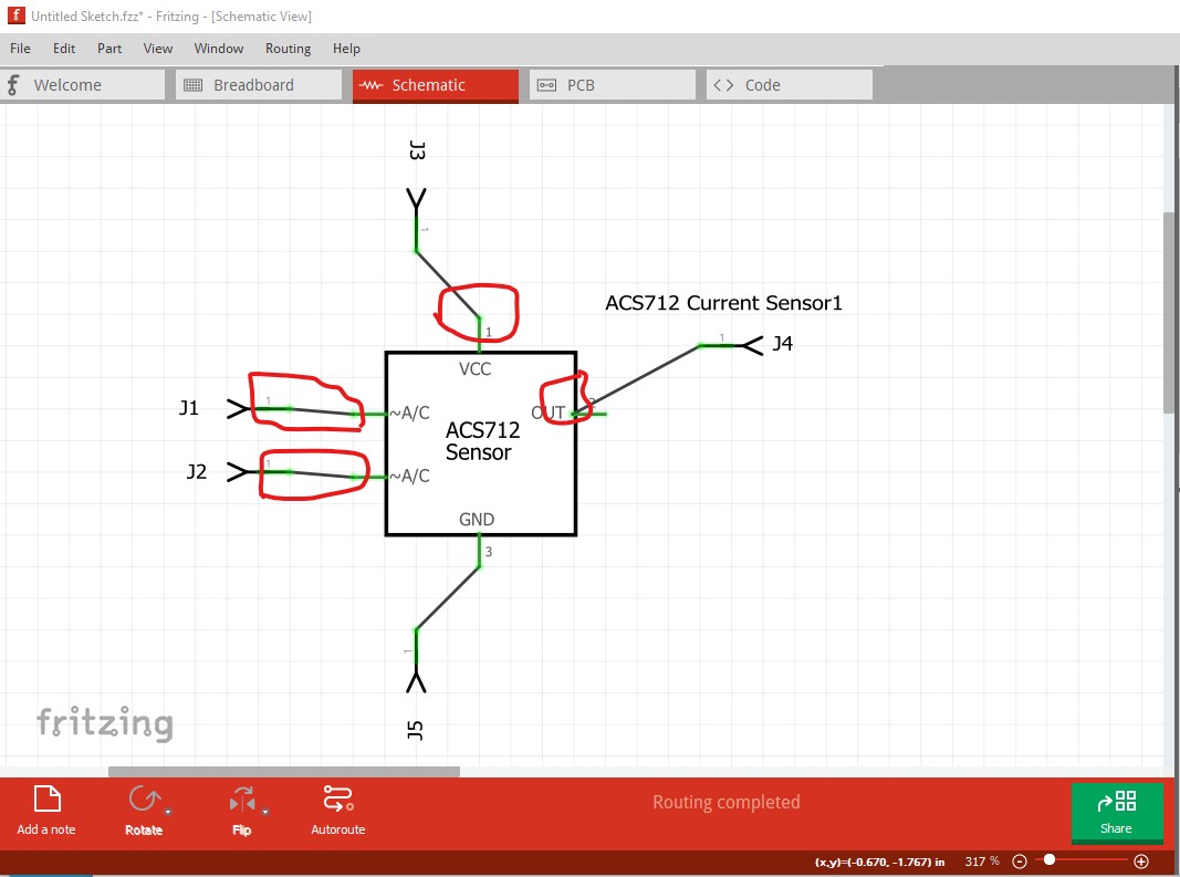
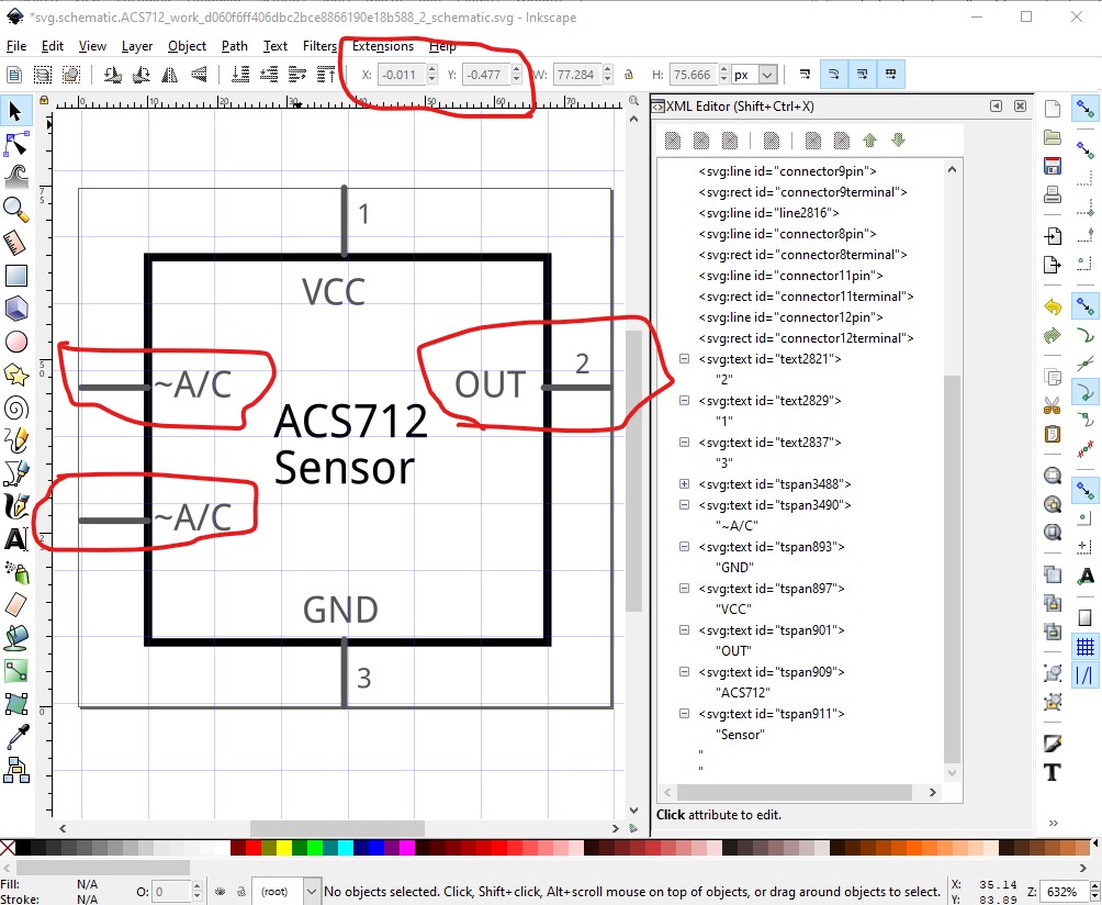
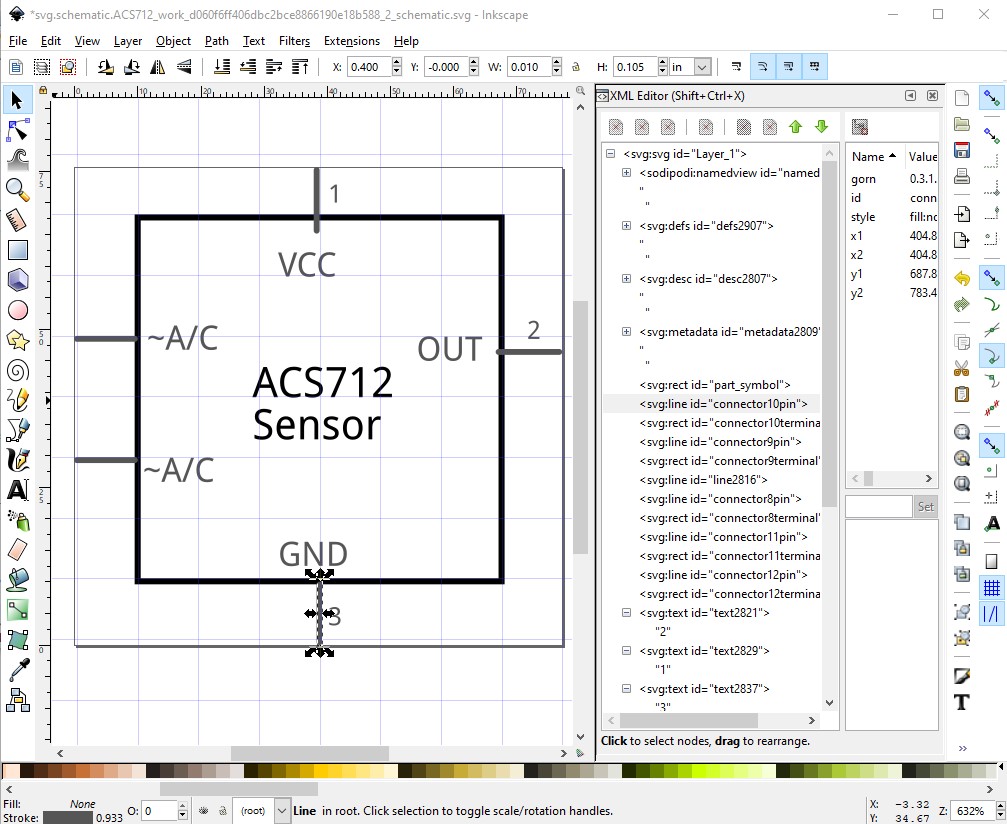
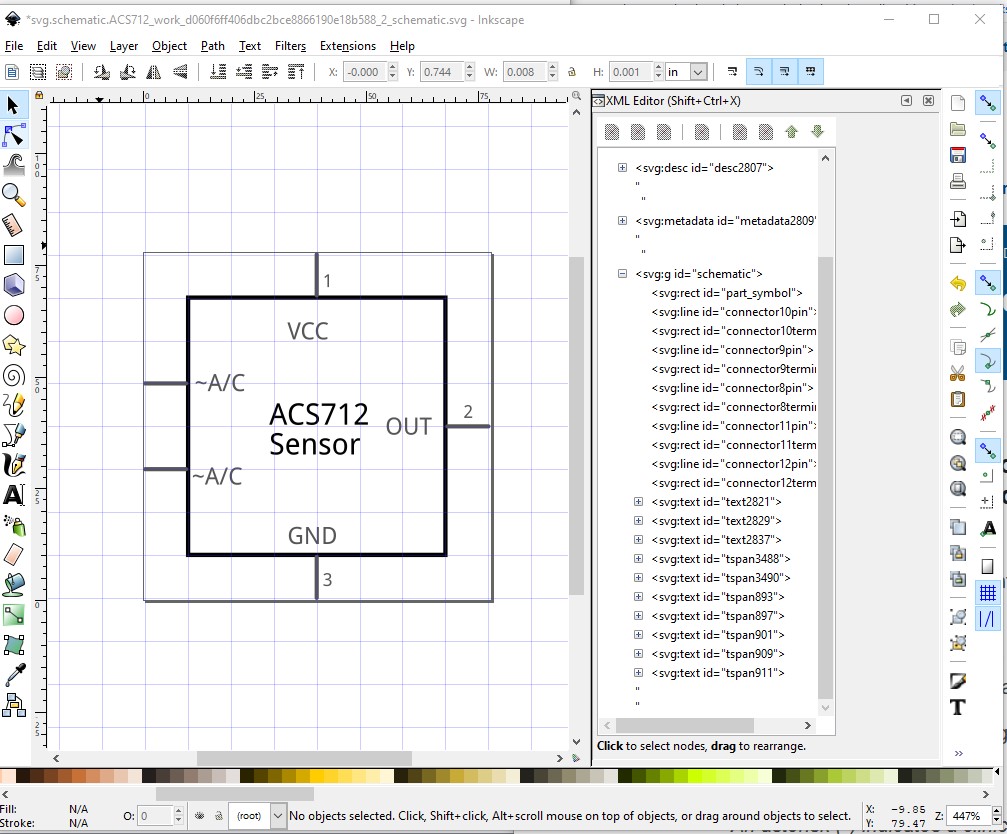
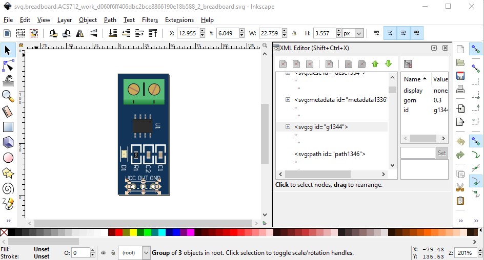
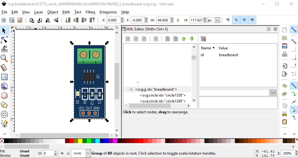
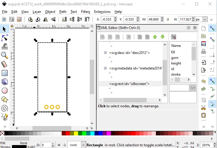
ACS712 Current Sensor has a number of problems:
schematic is misaligned
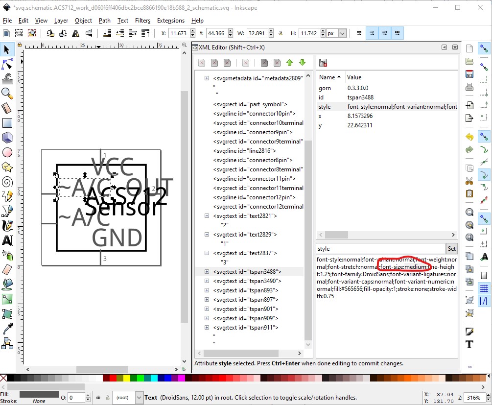
ungroup to adjust the alignment causes this:
for some reason ungrouping the tspans has caused font-size to change from 4px to medium (which is obviously wrong.)
correct the font sizes, add a .1 in grid and we see the alignent problem, the horizontal lines are not aligned to the .1 in grid
as well the drawing origin is not 0 0, so at least in Inkscape (I don’t know how to do this or if it is even possible in Illustrator) resize the page to selection to 0 0
First correct the rectangle to be on .1in boundaries
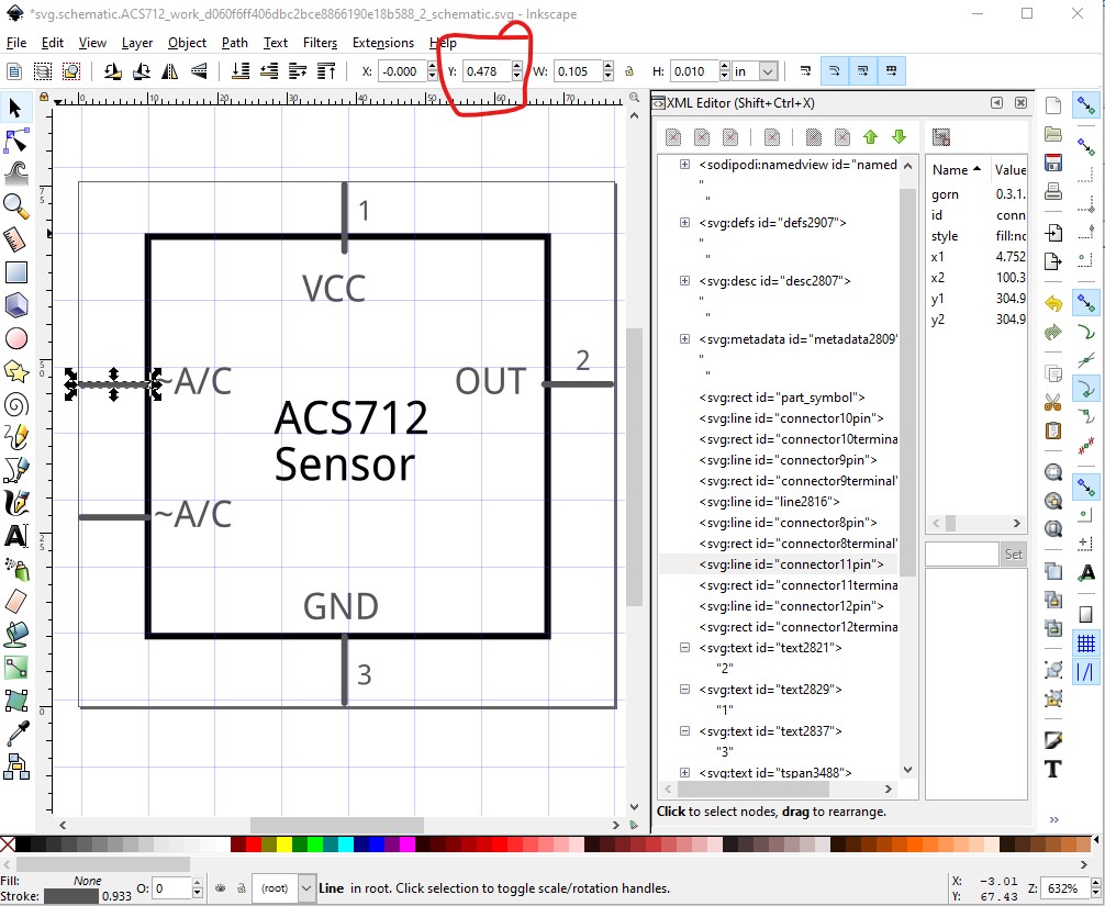
Now we switch to the top ac pin and see it is misaligned.
Its current y position is 0.478in instead of the 0.5in it needs to be to be in the .1in grid. So correct that.
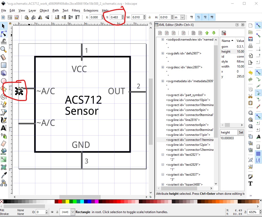
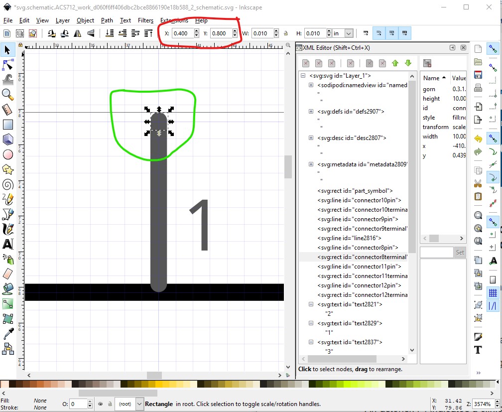
Then select connector11terminal, set it to be 10thou by 10thou and move it to also be at 0.5in to match the pin. Now correct the position of connector10pin (only 0.05in out in X):
to be exactly on the .1in boundary and do the same to connector10terminal.
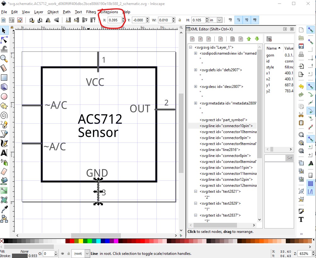
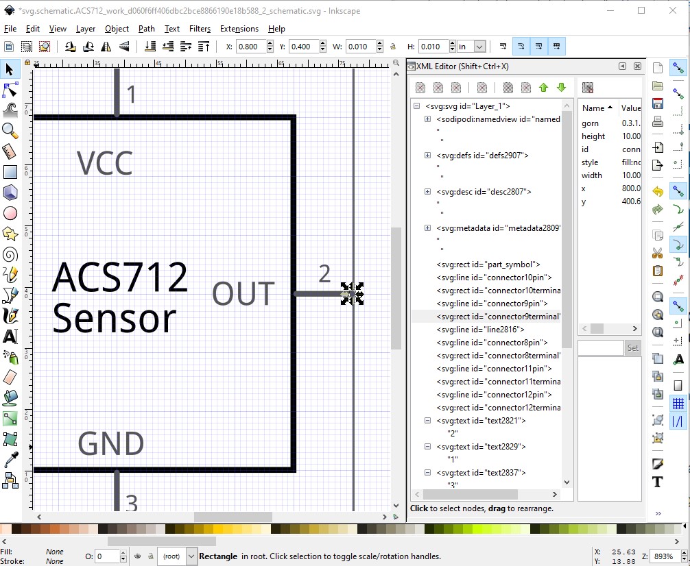
Now the top connector connector8 pin and terminal. The top and right pins are somewhat odd, in that they need an additional 0.05in added to their position to account for the 10thou width of the rectangle (the terminal does not get this correction!) So connector8pin goes from
to
while connector8terminal goes to 0.4 by 0.8in so as to be exactly centered on the grid lines at 0.1in.
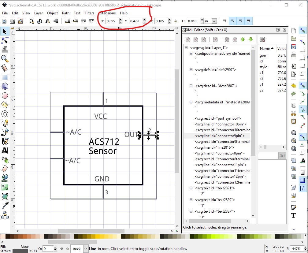
Now for connector9pin. As with connector8pin connector9’s x start wants to be 0.05in greater to account for the stroke-width of the rectangle, and it wants to move down a bit to be in the center of the rectangle like this
which changes to
we then edit select all, resize page to selection and group, then change the groupid to schematic and save the result as plain svg to have the corrected schematic svg.
Complaints from FritzingCheckPart.py
Error 69: File
‘svg.breadboard.ACS712_work_d060f6ff406dbc2bce8866190e18b588_2_breadboard.svg.bak’
At line 803
Found a drawing element before a layerId (or no layerId)
the breadboard svg has no group named breadboard. The effect of this is the part won’t export as an image (pdf, svg, jpeg etc.)
the fix is to do an edit select all, then group and name the group breadboard like this:
Warning 27: File
‘svg.pcb.ACS712_work_d060f6ff406dbc2bce8866190e18b588_2_pcb.svg.bak’
At line 709
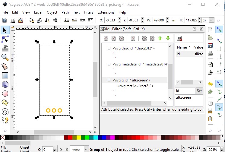
Fritzing layerId silkscreen isn’t a group which it usually should be
silkscreen isn’t a group which it should be (this works, but is incorrect)
fix it by grouping the rectangle and naming the group silkscreen
Modified 2: File
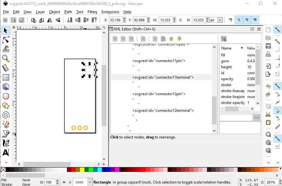
‘svg.pcb.ACS712_work_d060f6ff406dbc2bce8866190e18b588_2_pcb.svg.bak’
At line 716
Connector connector11terminal had a zero width, set to 10
Check the alignment of this pin in the svg!
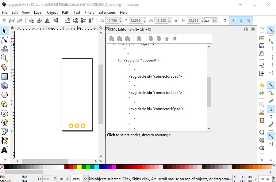
this is caused by the unused screw terminal connectors exisiting in the pcb svg. The solution is to just delete the unused connectors:
all these changes are in this part:
ACS712 Current Sensor-improved.fzpz (31.7 KB)
which looks better in schematic:
Peter