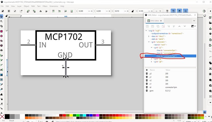
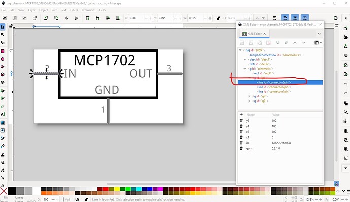
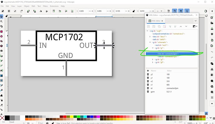
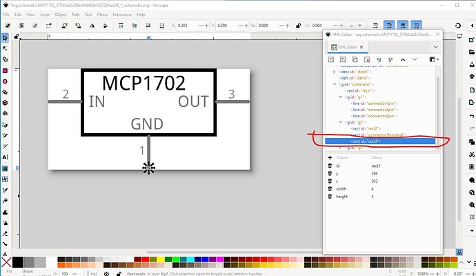
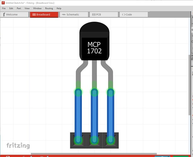
A few problems (mostly from bad practices in core parts to do with reusing svgs by scewing up fzp files.) To start I ran your part through FritzingCheckPart.py to see what errors (if any) it flagged. It has a few:
$ FritzingCheckPartw.py part.MCP1702_3f51a43a0b9f774a478536a3bf8c4789_4.fzp
**** Starting to process file Startup, no file yet
**** Starting to process file part.MCP1702_3f51a43a0b9f774a478536a3bf8c4789_4.fzp
**** Starting to process file svg.breadboard.MCP1702_57955dd535fad496f68bf28725fea348_1_breadboard.svg.bak
**** Starting to process file svg.schematic.MCP1702_57955dd535fad496f68bf28725fea348_1_schematic.svg.bak
**** Starting to process file svg.pcb.MCP1702_57955dd535fad496f68bf28725fea348_1_pcb.svg.bak
File
‘part.MCP1702_3f51a43a0b9f774a478536a3bf8c4789_4.fzp.bak’
This is a through hole part as both copper0 and copper1 views are present.
If you wanted a smd part remove the copper0 definition from line 52
Modified 4: File
‘svg.breadboard.MCP1702_57955dd535fad496f68bf28725fea348_1_breadboard.svg.bak’
At line 6
ReferenceFile
‘mcp1702_breadboard.svg’
doesn’t match input file
‘MCP1702_57955dd535fad496f68bf28725fea348_1_breadboard.svg’
Corrected
Modified 4: File
‘svg.schematic.MCP1702_57955dd535fad496f68bf28725fea348_1_schematic.svg.bak’
At line 4
ReferenceFile
‘MCP1702_voltage_regulator_to-92_schematic.svg’
doesn’t match input file
‘MCP1702_57955dd535fad496f68bf28725fea348_1_schematic.svg’
Corrected
Modified 4: File
‘svg.pcb.MCP1702_57955dd535fad496f68bf28725fea348_1_pcb.svg.bak’
At line 4
ReferenceFile
‘TO92_3_100mil_pcb.svg’
doesn’t match input file
‘MCP1702_57955dd535fad496f68bf28725fea348_1_pcb.svg’
Corrected
Modified 3: File
‘svg.pcb.MCP1702_57955dd535fad496f68bf28725fea348_1_pcb.svg.bak’
At line 8
Silkscreen, converted stoke from white to black
Modified 3: File
‘svg.pcb.MCP1702_57955dd535fad496f68bf28725fea348_1_pcb.svg.bak’
At line 9
Silkscreen, converted stoke from white to black
Warning 6: File
‘part.MCP1702_3f51a43a0b9f774a478536a3bf8c4789_4.fzp.bak’
At line 2
ReferenceFile name
‘MCP1702.fzp’
Doesn’t match fzp filename
‘MCP1702_3f51a43a0b9f774a478536a3bf8c4789_4.fzp’
Warning 13: File
‘part.MCP1702_3f51a43a0b9f774a478536a3bf8c4789_4.fzp.bak’
At line 66
Value connector1pin doesn’t match Id connector0. (Typo?)
Warning 13: File
‘part.MCP1702_3f51a43a0b9f774a478536a3bf8c4789_4.fzp.bak’
At line 66
Value connector1terminal doesn’t match Id connector0. (Typo?)
Warning 13: File
‘part.MCP1702_3f51a43a0b9f774a478536a3bf8c4789_4.fzp.bak’
At line 69
Value connector2pin doesn’t match Id connector0. (Typo?)
Warning 13: File
‘part.MCP1702_3f51a43a0b9f774a478536a3bf8c4789_4.fzp.bak’
At line 70
Value connector2pin doesn’t match Id connector0. (Typo?)
Warning 13: File
‘part.MCP1702_3f51a43a0b9f774a478536a3bf8c4789_4.fzp.bak’
At line 81
Value connector0pin doesn’t match Id connector1. (Typo?)
Warning 13: File
‘part.MCP1702_3f51a43a0b9f774a478536a3bf8c4789_4.fzp.bak’
At line 81
Value connector0terminal doesn’t match Id connector1. (Typo?)
Warning 13: File
‘part.MCP1702_3f51a43a0b9f774a478536a3bf8c4789_4.fzp.bak’
At line 99
Value connector0pin doesn’t match Id connector2. (Typo?)
Warning 13: File
‘part.MCP1702_3f51a43a0b9f774a478536a3bf8c4789_4.fzp.bak’
At line 100
Value connector0pin doesn’t match Id connector2. (Typo?)
Warning 32: File
‘svg.breadboard.MCP1702_57955dd535fad496f68bf28725fea348_1_breadboard.svg.bak’
At line 4
Scale is not the desirable 1/1000 ratio from width/height to
viewBox width/height.
Warning 24: File
‘svg.breadboard.MCP1702_57955dd535fad496f68bf28725fea348_1_breadboard.svg.bak’
At line 26
Font family ‘OCRAStd’ is not Droid Sans or OCRA
This won’t render in Fritzing
Error 18: File
‘part.MCP1702_3f51a43a0b9f774a478536a3bf8c4789_4.fzp.bak’
Connector connector1terminal is in the fzp file but not the svg file. (typo?)
svg svg.schematic.MCP1702_57955dd535fad496f68bf28725fea348_1_schematic.svg.bak
Error 18: File
‘part.MCP1702_3f51a43a0b9f774a478536a3bf8c4789_4.fzp.bak’
Connector connector0terminal is in the fzp file but not the svg file. (typo?)
svg svg.schematic.MCP1702_57955dd535fad496f68bf28725fea348_1_schematic.svg.bak
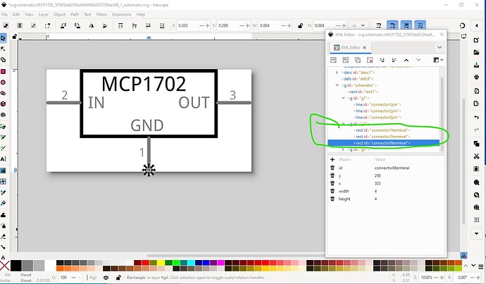
warnings won’t usually cause errors (in this case they do though) but errors will, although in this case in Fritzing 1.0.4 (and possibly earlier versions) they will be automatically corrected. The terminalIds are missing in schematic which will normally cause the wire to connect in the middle of the pin rather than the end (as noted in 1.0.4 this usually gets automtically corrected as a common error.) The breadboard svg is fine as is. The pins are correctly defined in the correct order. Schematic however has problems:
pin1 should be connector0pin but is connector2pin and so won’t match breadboard
pin2 should be connector1pin (and again won’t match breadboard.)
pin3 is correct as stands.
this rectangle should be connector0terminal (and is the cause of the terminalId missing error in FritizngCheckPart.py
This is the terminalIds corrected to match the pin numbers and breadboard.
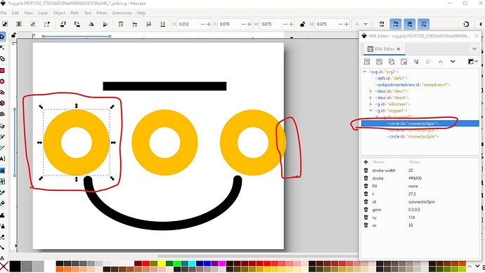
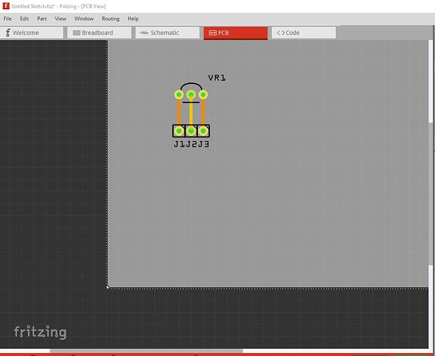
Changing to the pcb svg there are a couple of errors (as noted from core parts) first the svg hasn’t had the viewbox resized so the edge of the connector2pin will be truncated because it is outside the viewbox. Also the pins are in the wrong order and the silkscreen is inverted (because the original svg in core parts is badly configured)
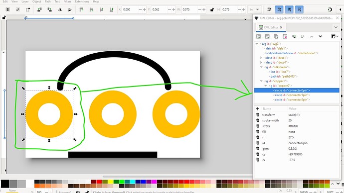
this is the corrected (to match breaboard) svg, connector0 is on the left and the silkscreen is inverted so the to92 orientation on silkscreen will be correct. That means we need to fix up the .fzp file so it matches this.
from
  <connectors>
    <connector id="connector0" name="GND" type="male">
      <description>Ground</description>
      <views>
        <breadboardView>
          <p layer="breadboard" legId="connector0leg" svgId="connector0pin"/>
        </breadboardView>
        <schematicView>
          <p layer="schematic" svgId="connector1pin" terminalId="connector1terminal"/>
        </schematicView>
        <pcbView>
          <p layer="copper0" svgId="connector2pin"/>
          <p layer="copper1" svgId="connector2pin"/>
        </pcbView>
      </views>
    </connector>
to
  <connectors>
    <connector id="connector0" name="GND" type="male">
      <description>Ground</description>
      <views>
        <breadboardView>
          <p layer="breadboard" legId="connector0leg" svgId="connector0pin"/>
        </breadboardView>
        <schematicView>
          <p layer="schematic" svgId="connector0pin" terminalId="connector0terminal"/>
        </schematicView>
        <pcbView>
          <p layer="copper0" svgId="connector0pin"/>
          <p layer="copper1" svgId="connector0pin"/>
        </pcbView>
      </views>
    </connector>
Where the connector number in all cases matches the connector definition rather than changes by view (which is confusing and in my view wrong.) The same needs to be done for the other 2 pin definitions.
from
    <connector id="connector1" name="Vin" type="male">
      <description>input voltage</description>
      <views>
        <breadboardView>
          <p layer="breadboard" legId="connector1leg" svgId="connector1pin"/>
        </breadboardView>
        <schematicView>
          <p layer="schematic" svgId="connector0pin" terminalId="connector0terminal"/>
        </schematicView>
        <pcbView>
          <p layer="copper0" svgId="connector1pin"/>
          <p layer="copper1" svgId="connector1pin"/>
        </pcbView>
      </views>
    </connector>
to
    <connector id="connector1" name="Vin" type="male">
      <description>input voltage</description>
      <views>
        <breadboardView>
          <p layer="breadboard" legId="connector1leg" svgId="connector1pin"/>
        </breadboardView>
        <schematicView>
          <p layer="schematic" svgId="connector1pin" terminalId="connector1terminal"/>
        </schematicView>
        <pcbView>
          <p layer="copper0" svgId="connector1pin"/>
          <p layer="copper1" svgId="connector1pin"/>
        </pcbView>
      </views>
    </connector>
from
    <connector id="connector2" name="Vout" type="male">
      <description>output voltage</description>
      <views>
        <breadboardView>
          <p layer="breadboard" legId="connector2leg" svgId="connector2pin"/>
        </breadboardView>
        <schematicView>
          <p layer="schematic" svgId="connector2pin" terminalId="connector2terminal"/>
        </schematicView>
        <pcbView>
          <p layer="copper0" svgId="connector0pin"/>
          <p layer="copper1" svgId="connector0pin"/>
        </pcbView>
      </views>
    </connector>
to
    <connector id="connector2" name="Vout" type="male">
      <description>output voltage</description>
      <views>
        <breadboardView>
          <p layer="breadboard" legId="connector2leg" svgId="connector2pin"/>
        </breadboardView>
        <schematicView>
          <p layer="schematic" svgId="connector2pin" terminalId="connector2terminal"/>
        </schematicView>
        <pcbView>
          <p layer="copper0" svgId="connector2pin"/>
          <p layer="copper1" svgId="connector2pin"/>
        </pcbView>
      </views>
    </connector>
With these changes FritzingCheckPart.py gives some warnings but no errors:
$ FritzingCheckPartw.py part.MCP1702_3f51a43a0b9f774a478536a3bf8c4789_4.fzp
**** Starting to process file Startup, no file yet
**** Starting to process file part.MCP1702_3f51a43a0b9f774a478536a3bf8c4789_4.fzp
**** Starting to process file svg.breadboard.MCP1702_57955dd535fad496f68bf28725fea348_1_breadboard.svg.bak
**** Starting to process file svg.schematic.MCP1702_57955dd535fad496f68bf28725fea348_1_schematic.svg.bak
**** Starting to process file svg.pcb.MCP1702_57955dd535fad496f68bf28725fea348_1_pcb.svg.bak
File
‘part.MCP1702_3f51a43a0b9f774a478536a3bf8c4789_4.fzp.bak’
This is a through hole part as both copper0 and copper1 views are present.
If you wanted a smd part remove the copper0 definition from line 52
Modified 4: File
‘svg.schematic.MCP1702_57955dd535fad496f68bf28725fea348_1_schematic.svg.bak’
At line 13
ReferenceFile
‘MCP1702_voltage_regulator_to-92_schematic.svg’
doesn’t match input file
‘MCP1702_57955dd535fad496f68bf28725fea348_1_schematic.svg’
Corrected
Modified 1: File
‘svg.schematic.MCP1702_57955dd535fad496f68bf28725fea348_1_schematic.svg.bak’
At line 35
Removed px from font-size leaving 60
Modified 1: File
‘svg.schematic.MCP1702_57955dd535fad496f68bf28725fea348_1_schematic.svg.bak’
At line 42
Removed px from font-size leaving 48
Modified 1: File
‘svg.schematic.MCP1702_57955dd535fad496f68bf28725fea348_1_schematic.svg.bak’
At line 49
Removed px from font-size leaving 48
Modified 1: File
‘svg.schematic.MCP1702_57955dd535fad496f68bf28725fea348_1_schematic.svg.bak’
At line 56
Removed px from font-size leaving 48
Modified 1: File
‘svg.schematic.MCP1702_57955dd535fad496f68bf28725fea348_1_schematic.svg.bak’
At line 63
Removed px from font-size leaving 36
Modified 1: File
‘svg.schematic.MCP1702_57955dd535fad496f68bf28725fea348_1_schematic.svg.bak’
At line 70
Removed px from font-size leaving 36
Modified 1: File
‘svg.schematic.MCP1702_57955dd535fad496f68bf28725fea348_1_schematic.svg.bak’
At line 77
Removed px from font-size leaving 36
Warning 6: File
‘part.MCP1702_3f51a43a0b9f774a478536a3bf8c4789_4.fzp.bak’
At line 2
ReferenceFile name
‘MCP1702.fzp’
Doesn’t match fzp filename
‘MCP1702_3f51a43a0b9f774a478536a3bf8c4789_4.fzp’
Warning 32: File
‘svg.breadboard.MCP1702_57955dd535fad496f68bf28725fea348_1_breadboard.svg.bak’
At line 16
Scale is not the desirable 1/1000 ratio from width/height to
viewBox width/height.
Warning 24: File
‘svg.breadboard.MCP1702_57955dd535fad496f68bf28725fea348_1_breadboard.svg.bak’
At line 156
Font family ‘OCRAStd’ is not Droid Sans or OCRA
This won’t render in Fritzing
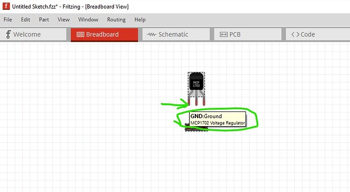
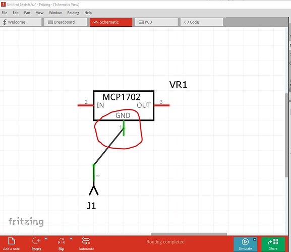
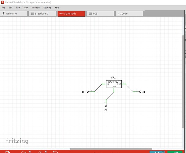
I could remove the remaining warnings by correcting the issues, but it won’t make any difference (Fritzing will correct the issues.) This is your original part in Fritzing (it mostly works except for the terminalIds) Pin1 is correctly identified (as all are because of the modified fzp file)
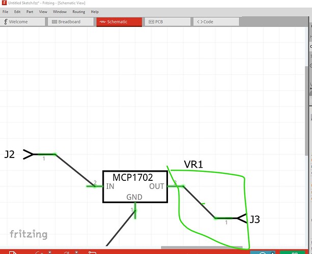
but in schematic the lack of terminalId causes the wire to connect to the center of the pin (automatic correction didn’t kick in for some reason)
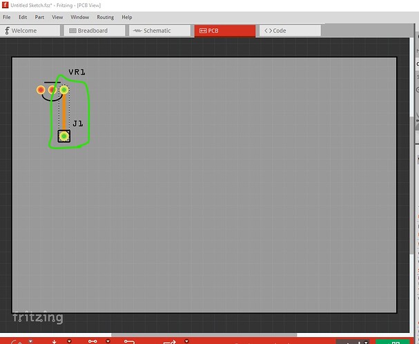
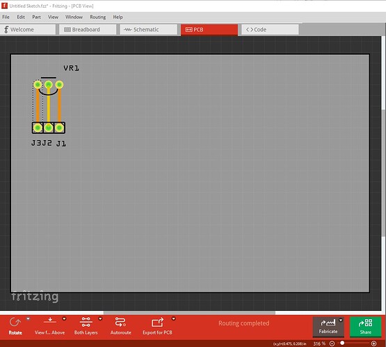
and pcb is fine
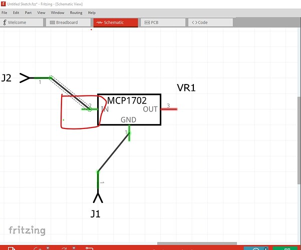
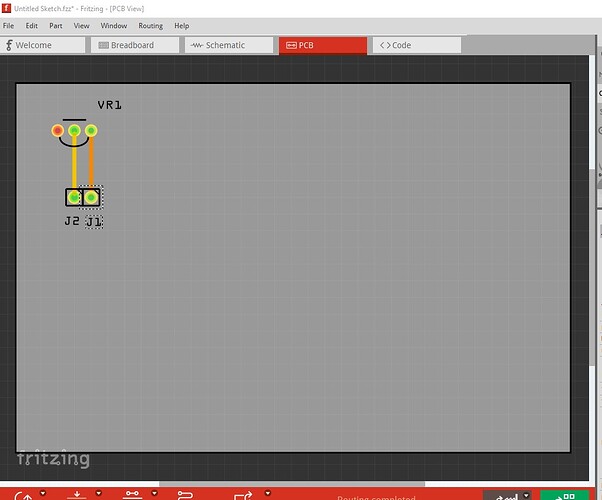
Same for pin2
and pin3 is entirely correct
because it has a teminalId defined schematic is correct.
Now load this part
MCP1702 Voltage Regulator-fixed.fzpz (6.2 KB)
(to load it you will first need to delete the current part from the mine parts bin then shutdown and restart Fritzing to really delete the part.)
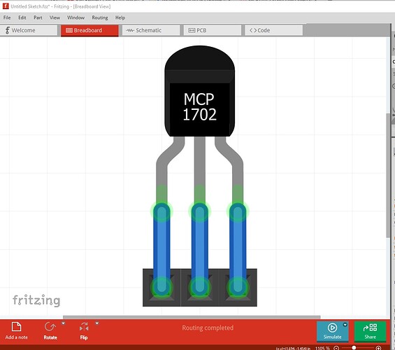
which looks like this
Not a lot of visible change (other than schematic) but the part is now much easier to modify.
Peter
